Fairchild FAN6756 service manual

FAN6756 — mWSaver™ PWM Controller
FAN6756 — mWSaver™ PWM Controller
May 2012
Features
Single-Ended Topologies, such as Flyback and
Forward Converters
mWSaver™ Technology
- Achieves Low No-Load Power Consumption:
Less than 30mW at 230V
Included)
(EMI Filter Loss
AC
- Eliminates X Capacitor Discharge Resistor Loss
with AX-CAP™ Technology
- Linearly Decreases Switching Frequency to
23KHz
- Burst Mode Operation at Light-Load Condition
- Impedance Modulation in Standby Mode for
“Deep” Burst Mode Operation
- Low Operating Current (450µA) in Standby Mode
- 500V High-Voltage JFET Startup Circuit to
Eliminate Startup Resistor Loss
Highly Integrated with Rich Features
- Proprietary Frequency Hopping to Reduce EMI
- High-Voltage Sampling to Detect Input Voltage
- Peak-Current-Mode Control with Slope
Compensation
- Cycle-by-Cycle Current Limiting with Line
Compensation
- Leading Edge Blanking (LEB)
- Built-In 8ms Soft-Start
Advanced Protections
- Brown-In/Brownout Recovery
- Internal Overload/Open-Loop Protection (OLP)
- V
Under-Voltage Lockout (UVLO)
DD
- V
Over-Voltage Protection (V
DD
DD
OVP)
- Over-Temperature Protection (OTP)
- Current-Sense Short-Circuit Protection (SSCP)
Description
The FAN6756 is a next-generation Green Mode PWM
controller with innovative mWSaver™ technology, which
dramatically reduces standby and no-load power
consumption, enabling conformance to worldwide
Standby Mode efficiency guidelines.
An innovative AX-CAP™ method minimizes losses in
the EMI filter stage by eliminating the X-cap discharge
resistors while meeting IEC61010-1 safety
requirements. Standby Mode clamps feedback voltage
and modulates feedback impedance with an impedance
modulator during Burst Mode operation, which forces
the system to operate in a “deep” Burst Mode with
minimum switching losses.
Protections ensure safe operation of power system in
various abnormal conditions. Proprietary frequencyhopping function decreases EMI emission and built-in
synchronized slope compensation allows more stable
Peak-Current-Mode control over wide range of input
voltage and load conditions. The proprietary internal line
compensation ensures constant output power limit over
entire universal line voltage range.
Requiring a minimum number of external components,
FAN6756 provides a basic platform that is well suited for
cost-effective flyback converter designs that require
extremely low standby power consumption.
Applications
Flyback power supplies that demand extremely low
standby power consumption, such as:
Adapters for Notebooks, Printers, Game Consoles,
etc.
Open-Frame SMPS for LCD TV, LCD Monitors,
Printer Power, etc.
Related Resources
Evaluation Board: FEBFAN6756MR_T03U065A
Ordering Information
Part Number
Protections
OLP OVP OTP SSCP
FAN6756MRMY A/R L L A/R
FAN6756MLMY L L L A/R
Note:
1. A/R = Auto Recovery Mode protection, L = Latch Mode protection.
© 2011 Fairchild Semiconductor Corporation www.fairchildsemi.com
FAN6756 • Rev. 1.0.7
(1)
Operating
Temperature Range
-40 to +105°C
Package
8-Pin, Small Outline
Package (SOP)
Packing
Method
Tape & Reel

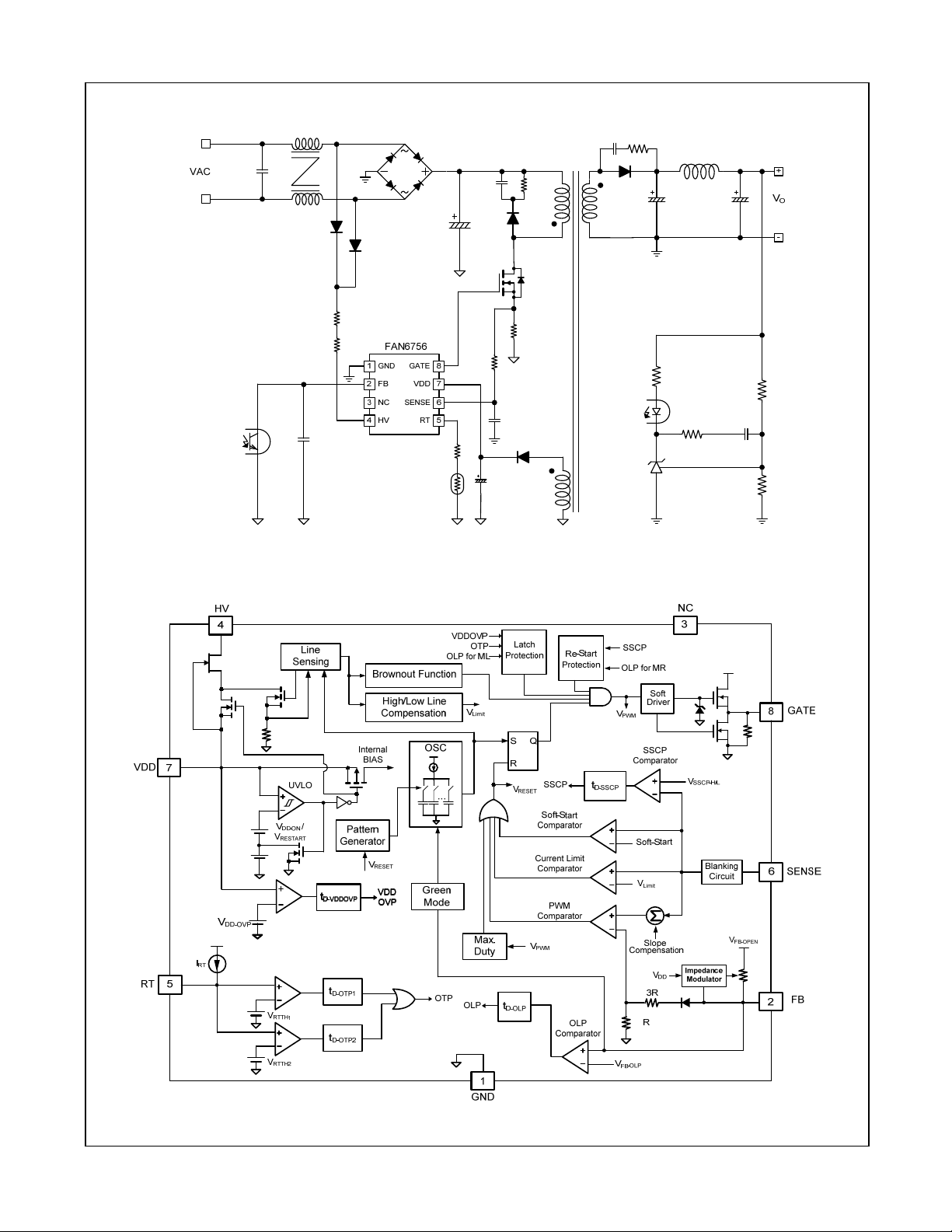
Application Diagram
FAN6756 — mWSaver™ PWM Controller
Internal Block Diagram
Figure 1. Typical Application Diagram
Figure 2. Functional Block Diagram
© 2011 Fairchild Semiconductor Corporation www.fairchildsemi.com
FAN6756 • Rev. 1.0.7 2

Marking Information
ZXYTT
6756ML
TPM
Pin Configuration
ZXYTT
6756MR
TPM
FAN6756 — mWSaver™ PWM Controller
F - Fairchild Logo
Z - Plant Code
X - 1-Digit Year Code
Y - 1-Digit Week Code
TT - 2-Digit Die Run Code
T - Package Type (M=SOP)
P - Y: Green Package
M - Manufacture Flow Code
Figure 3. Top Mark
SOP-8
GND
FB
NC
HV
18
2
3
GATE
7
6
54
VDD
SENSE
RT
Figure 4. Pin Configuration (Top View)
Pin Definitions
Pin # Name Description
1 GND Ground Pin. Placing a 0.1µF decoupling capacitor between VDD and GND is recommended.
Feedback Pin. The output voltage feedback information from the external compensation circuit is
2 FB
3 NC No Connection
4 HV
5 RT
6 SENSE
7 VDD
8 GATE
fed into this pin. The PWM duty cycle is determined by comparing the FB signal with the currentsense signal from the SENSE pin.
High-Voltage Startup. The HV pin is typically connected to the AC line input through two external
diodes and one resistor (R
). This pin is used, not only to charge the VDD capacitor during
HV
startup, but also to sense the line voltage. The line voltage information is used for brownout
protection and power limit line compensation. This pin also is used to intelligently discharge the
EMI filter capacitor when the removal of the AC line voltage is detected.
Over-Temperature Protection. An external NTC thermistor is connected from this pin to the GND
pin. Once the voltage of the RT pin drops below the threshold voltage, the controller latches off
the PWM. The RT pin also provides external latch protection. If the RT pin is not connected to
the NTC resistor for over-temperature protection, it is recommended to place a 100k resistor to
ground to prevent noise interference.
Current Sense. The sensed voltage is used for Peak-Current-Mode control, short-circuit
protection, and cycle-by-cycle current limiting.
Power Supply of IC. Typically a hold-up capacitor connects from this pin to ground. A rectifier
diode, in series with the transformer auxiliary winding, connects to this pin to supply bias during
normal operation.
Gate Drive Output. The totem-pole output driver for the power MOSFET; internally limited to
V
GATE-CLAMP
.
© 2011 Fairchild Semiconductor Corporation www.fairchildsemi.com
FAN6756 • Rev. 1.0.7 3

FAN6756 — mWSaver™ PWM Controller
Absolute Maximum Ratings
Stresses exceeding the absolute maximum ratings may damage the device. The device may not function or be
operable above the recommended operating conditions and stressing the parts to these levels is not recommended.
In addition, extended exposure to stresses above the recommended operating conditions may affect device reliability.
The absolute maximum ratings are stress ratings only.
Symbol Parameter Min. Max. Unit
VDD DC Supply Voltage
VFB FB Pin Input Voltage -0.3 7.0 V
V
SENSE Pin Input Voltage -0.3 7.0 V
SENSE
VRT RT Pin Input Voltage -0.3 7.0 V
VHV HV Pin Input Voltage 500 V
PD
ΘJA
Power Dissipation (TA=50°C)
Thermal Resistance (Junction-to-Air) 150
TJ Operating Junction Temperature -40 +125
T
Storage Temperature Range -55 +150
STG
TL Lead Temperature (Wave Soldering or IR, 10 Seconds) +260
Human Body Model,
ESD
JEDEC:JESD22-A114
Charged Device Model,
JEDEC:JESD22-C101
Notes:
2. All voltage values, except differential voltages, are given with respect to the network ground terminal.
3. Stresses beyond those listed under Absolute Maximum Ratings may cause permanent damage to the device.
4. ESD level with the HV pin is CDM=1250V and HBM=500V.
(2,3)
30 V
400 mW
°C/W
°C
°C
°C
All Pins Except HV Pin
(4)
6000
V
All Pins Except HV Pin
(4)
2000
Recommended Operating Conditions
The Recommended Operating Conditions table defines the conditions for actual device operation. Recommended
operating conditions are specified to ensure optimal performance to the datasheet specifications. Fairchild does not
recommend exceeding them or designing to Absolute Maximum Ratings.
Symbol Parameter Min. Typ. Max. Unit
RHV Resistance on HV Pin 150 200 250 k
© 2011 Fairchild Semiconductor Corporation www.fairchildsemi.com
FAN6756 • Rev. 1.0.7 4

FAN6756 — mWSaver™ PWM Controller
Electrical Characteristics
VDD=15V and TA=25°C unless otherwise noted.
Symbol Parameter Condition Min. Typ. Max. Unit
VDD Section
VOP Continuously Operating Voltage Limited by VDD OVP 22 V
V
Threshold Voltage to Startup VDD Rising 16 17 18 V
DD-ON
V
DD-OFF
V
DD-OLP
V
UVLO
V
RESTART
V
DD-LH
V
DD-AC
I
DD-ST
I
DD-OP1
ILH
I
DD-OP2
I
DD-OLP
V
DD-OVP
t
D-VDDOVP
Threshold Voltage to Stop Switching
in Protection Mode
Threshold Voltage to Turn-on HV
Startup in Protection Mode
Threshold Voltage to Stop Switching
in Normal Mode
V
Falling 10 11 12 V
DD
VDD Falling 6 7 8 V
VDD Falling 5.5 6.5 7.5 V
Threshold Voltage to Enable HV
Startup to charge VDD in Normal
VDD Falling 5 V
Mode
Threshold Voltage to Release Latch
Mode
VDD Falling 3.5 4.0 4.5 V
Threshold Voltage for Brown-in 9.0 9.5 10.0 V
Startup Current V
Supply Current in PWM Operation
Operating Current when VDD<V
DD-OFF
in Protection Mode
Supply Current when PWM Stops
Internal Sink Current from V
V
in Protection Mode
DD-OLP
Threshold Voltage for VDD OverVoltage Protection
VDD Over-Voltage Protection
Debounce Time
DD-OFF
to
– 0.16V 30 µA
DD-ON
VDD=15V, VFB=3V,
Gate Open
1.8 mA
VDD=5V 70 µA
VDD=15V, VFB <1.4V,
Gate Off
+0.1V 160 210 260 µA
V
DD-OLP
450 µA
23.5 24.5 25.5 V
110 185 260 µs
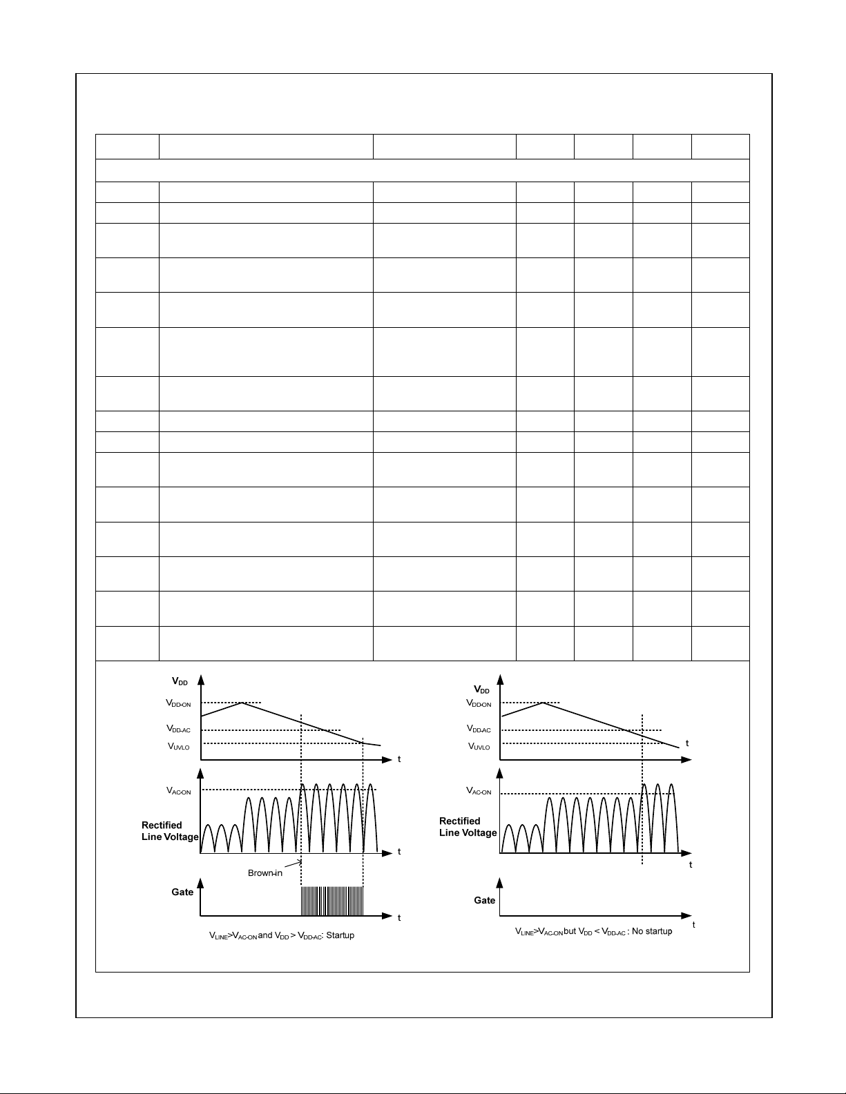
Figure 5. Timing Diagram for Brown-in Function
Continued on the following page…
© 2011 Fairchild Semiconductor Corporation www.fairchildsemi.com
FAN6756 • Rev. 1.0.7 5

FAN6756 — mWSaver™ PWM Controller
Electrical Characteristics (Continued)
VDD=15V and TA=25°C unless otherwise noted.
Symbol Parameter Condition Min. Typ. Max. Unit
HV Section
IHV Supply Current from HV Pin
V
Threshold Voltage for Brownout
AC-OFF
V
Threshold Voltage for Brown-In
AC-ON
△V
AC
t
D-AC-OFF
V
HV-DIS
t
D-HV-DIS
V
Debounce Time for Brownout 40 65 90 ms
AC-ON
- V
AC-OFF
X-Cap. Discharge Threshold
Debounce Time for Triggering
X-Cap. Discharge
Oscillator Section
f
OSC
t
HOP
f
OSC-G
fDV
fDT
Switching Frequency When
V
FB>VFB-N
Hopping Period VFB>V
Switching Frequency When
V
FB<VFB-G
Frequency Variation vs. VDD
Deviation
Frequency Variation vs.
Temperature Deviation
Feedback Input Section
AV
ZFB
V
FB-OPEN
V
FB-OLP
t
D-OLP
V
V
V
FB-ZDC1
V
FB-ZDCR1
V
FB-ZDC2
V
FB-ZDCR2
Feedback Voltage to CurrentSense Attenuation
Regular FB Internal Pull-High
Impedance
FB internal Biased Voltage FB Pin Open 5.2 5.4 5.6 V
Threshold Voltage for OLP 4.3 4.6 4.9 V
Debounce Time for OLP 45.0 57.5 70.0 ms
Threshold Voltage for Maximum
FB-N
Switching Frequency
Threshold Voltage for Minimum
FB-G
Switching Frequency
Threshold Voltage for Zero-Duty
Cycle
Threshold Voltage for Zero-Duty
Cycle Recovery
Threshold Voltage for Zero Duty
Cycle in Standby Mode
Threshold Voltage for Zero-Duty
Cycle Recovery in Standby Mode
VAC=90V (VDC=120V),
=0V
V
DD
DC Source Series
R=200k to HV Pin
DC Source Series
R=200k to HV Pin
DC Source Series
R=200k to HV Pin
VFB<V
FB-G
R=200k to HV Pin
30 40 50 ms
Center Frequency 62 65 68
Hopping Range
(V
FB>VFB-N
V
FB<VFB-G
)
4.0 6.5 ms
FB-N
20 23 26 kHz
VDD=11V to 22V 5 %
TA=-40 to 105°C
1/4.5 1/4.0 1/3.5 V/V
8.5 k
2.6 2.8 3.0 V
1.8 2.0 2.2 V
2.4 2.6 2.8 V
2.0 3.5 5.0
90 100 110
100 110 120
8 12 16
VDC
×0.45
(5)
V
DC
×0.51
VDC
×0.56
±3.7 ±4.2 ±4.7
mA
V
V
V
V
kHz
5 %
2.1
1.9
2.35
2.3 2.5 V
2.1 2.3 V
2.55 2.75 V
Continued on the following page…
© 2011 Fairchild Semiconductor Corporation www.fairchildsemi.com
FAN6756 • Rev. 1.0.7 6
 Loading...