Fairchild FAN6755W service manual
FAN6755W / FAN6755UW
mWSaver
™
PWM Controller
FAN6755W / FAN6755UW — mWSaver™ Controller
June 2011
Features
mWSaver
Class Standby Power
o <100mW at 25mW Load for LCDM Adaptor
o Internal High-Voltage JFET Startup
o Low Operating Current Maximum: 2mA
o Adaptive Decreasing of PWM Frequency to
o Feedback Impedance Switching During
™
Technology Provides Industry’s Best-in-
23KHz at Light-Load Condition, Improved
Light-Load Efficiency
Minimum Load or No Load
Proprietary Asynchronous Frequency Hopping
Reduced EMI
Fixed PWM Frequency: 65KHz (FAN6755W),
130KHz (FAN6755UW)
Internal Leading-Edge Blanking
Built-in Synchronized Slope Compensation
Auto-Restart Protection: Feedback Open-Loop
Protection (OLP), V
(OVP), Over-Temperature Protection (OTP), and
Line Over-Voltage Protection
Over-Voltage Protection
DD
Soft Gate Drive with Clamped Output Voltage: 18V
V
Under-Voltage Lockout (UVLO)
DD
Programmable Constant Power Limit (Full AC
Input Range)
Internal OTP Sensor with Hysteresis
Build-in 5ms Soft-Start Function
Input Voltage Sensing (V
Protection with Hysteresis and Line Over-Voltage
Protection
Pin) for Brown-In/Out
IN
Description
This highly integrated PWM controller provides several
features to enhance the performance of flyback
converters.
To minimize standby power consumption, a proprietary
adaptive green-mode function reduces switching
frequency at light-load condition. To avoid acousticnoise problems, the minimum PWM frequency is set
above 23kHz. This green-mode function enables the
power supply to meet international power conservation
requirements, such as Energy Star
high-voltage startup circuitry, the power loss caused by
bleeding resistors is also eliminated. To further reduce
power consumption, FAN6755W/UW uses the BiCMOS
process, which allows an operating current of only 2mA.
The standby power consumption can be under 100mW
for most of LCD monitor power supply designs.
FAN6755W/UW integrates a frequency-hopping function
that reduces EMI emission of a power supply with
minimum line filters. Its built-in synchronized slope
compensation achieves a stable peak-current-mode
control and improves noise immunity. The proprietary,
external line compensation ensures constant output
power limit over a wide AC input voltage range from
90V
to 264VAC.
AC
FAN6755W/UW provides many protection functions.
The internal feedback open-loop protection circuit
protects the power supply from open feedback loop
condition or output short condition. It also has line
under-voltage protection (brownout protection) and overvoltage protection using an input voltage sensing pin
(V
).
IN
FAN6755W/UW is available in a 7-pin SOP package.
®
. With the internal
Applications
General-purpose switched-mode power supplies and
flyback power converters, including:
LCD Monitor Power Supply
Open-Frame SMPS
ENERGY STAR® is a registered trademark of the U.S. Department of Energy and the U.S. Environmental Protection Agency.
© 2009 Fairchild Semiconductor Corporation www.fairchildsemi.com
FAN6755W / FAN6755UW • Rev. 1.0.5
Ordering Information
Operating
Part Number
Temperature
Package
Range
FAN6755WMY -40 to +105°C
FAN6755UWMY -40 to +105°C 130kHz Reel & Tape
7-Lead, Small Outline Integrated Circuit
(SOIC), Depopulated JEDEC MS-112, .150
Inch Body
PWM
Frequency
65kHz Reel & Tape
Packing
Method
Application Diagram
FAN6755W / FAN6755UW — mWSaver™ Controller
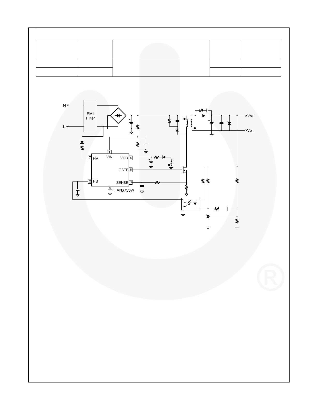
Figure 1. Typical Application
© 2009 Fairchild Semiconductor Corporation www.fairchildsemi.com
FAN6755W / FAN6755UW • Rev. 1.0.5 2
Internal Block Diagram
HV
7
HV
Startup
VDD
6
DD-OFF
/V
DD-ON
V
V
DD-OVP
V
/ V
IN_ON
IN_OFF
1
VIN
High/Low
Line Compensation
5.3V
UVLO
Debounce
Brownout Protection
Debounce
Re-start
OTP
4
GND
OLP
Protection
QS
R
Soft-Start
Comparator
Current Limit
Comparator
PWM
Comparator
OLP
Delay
Comparator
Brownout Protection
Clock
Generator
Internal
BIAS
OVP
V
Limit
V
rotect
IN-P
…
Green
Mode
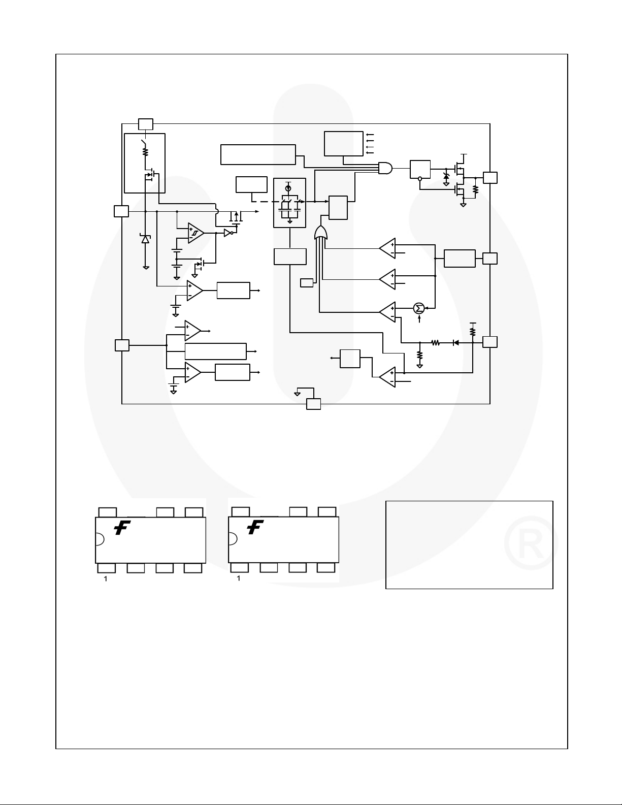
Figure 2. Internal Block Diagram
OLP
OTP
OVP
OLP
V
IN-P
rotect
Soft-Start
Compensation
Soft
Driver
V
Limit
Slope
R
V
FB-OLP
3R
V
DD
Circuit
Blanking
5.3V
5
3
2
FAN6755W / FAN6755UW — mWSaver™ Controller
GATE
SENSE
FB
Marking Information
ZXYTT
6755
WTPM
ZXYTT
6755U
WTPM
Figure 3. Top Mark
Z: Plant Code
X: 1-Digit Year Code
Y: 1-Digit Week Code
TT: 2-Digit Die Run Code
T: Package Type (M:SOP)
P: Y=Green Package
M: Manufacture Flow Code
© 2009 Fairchild Semiconductor Corporation www.fairchildsemi.com
FAN6755W / FAN6755UW • Rev. 1.0.5 3
Pin Configuration
VIN
FB
SENSE
GND
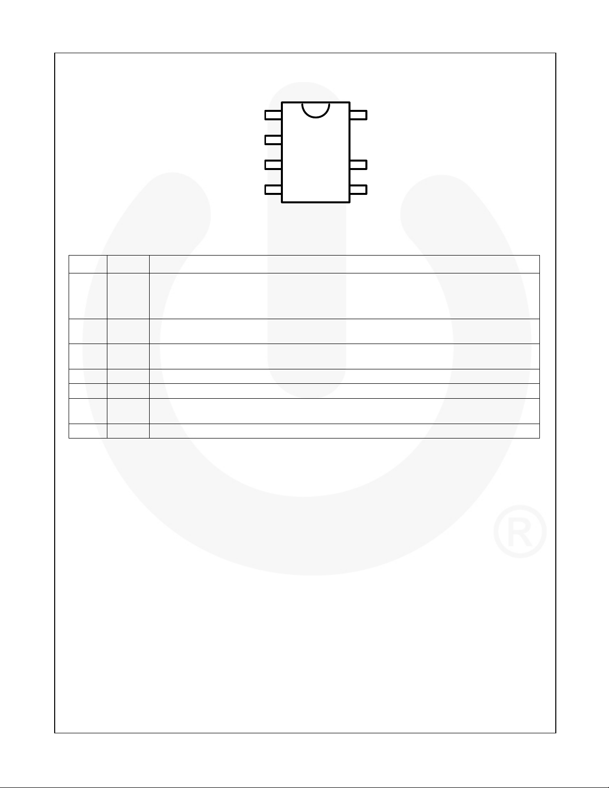
Figure 4. Pin Configuration (Top View)
SOP-7
17
HV
2
3
6
54
VDD
GATE
Pin Definitions
Pin # Name Description
Line-voltage detection. The line-voltage detection is used for brownout protection with hysteresis.
1 VIN
2 FB
3 SENSE
4 GND Ground
5 GATE The totem-pole output driver. Soft-driving waveform is implemented for improved EMI.
6 VDD
7 HV For startup, this pin is pulled HIGH to the line input or bulk capacitor via resistors.
Constant output power limit over universal AC input range is also achieved using this VIN pin. It
is suggested to add a low-pass filter to filter out line ripple on the bulk capacitor. Pulling VIN
HIGH also triggers auto-restart protection.
The signal from the external compensation circuit is fed into this pin. The PWM duty cycle is
determined in response to the signal on this pin and the current-sense signal on the SENSE pin.
Current sense. The sensed voltage is used for peak-current-mode control and cycle-by-cycle
current limiting.
Power supply. The internal protection circuit disables PWM output as long as V
OVP trigger point.
exceeds the
DD
FAN6755W / FAN6755UW — mWSaver™ Controller
© 2009 Fairchild Semiconductor Corporation www.fairchildsemi.com
FAN6755W / FAN6755UW • Rev. 1.0.5 4
FAN6755W / FAN6755UW — mWSaver™ Controller
Absolute Maximum Ratings
Stresses exceeding the absolute maximum ratings may damage the device. The device may not function or be
operable above the recommended operating conditions and stressing the parts to these levels is not recommended.
In addition, extended exposure to stresses above the recommended operating conditions may affect device reliability.
The absolute maximum ratings are stress ratings only.
Symbol Parameter Min. Max. Unit
V
DC Supply Voltage
VDD
VFB FB Pin Input Voltage -0.3 7.0 V
V
SENSE Pin Input Voltage -0.3 7.0 V
SENSE
V
VIN Pin Input Voltage -0.3 7.0 V
VIN
VHV HV Pin Input Voltage 700 V
PD
JA
Power Dissipation (T
Thermal Resistance (Junction-to-Air) 150
TJ Operating Junction Temperature -40 +125
T
Storage Temperature Range -55 +150
STG
TL Lead Temperature (Wave Soldering or IR, 10 Seconds) +260
Human Body Model,
ESD
JEDEC: JESD22-A114
Charged Device Model,
JEDEC: JESD22-C101
Notes:
1. All voltage values, except differential voltages, are given with respect to the network ground terminal.
2. Stresses beyond those listed under Absolute Maximum Ratings may cause permanent damage to the device.
3. ESD with HV pin: CDM=2000V (FAN6755W) or 1500V (FAN6755UW), and HBM=3500V.
(1, 2)
30 V
<50°C)
A
400 mW
C/W
C
C
C
All Pins Except HV Pin 5.5
kV
All Pins Except HV Pin 2.0
© 2009 Fairchild Semiconductor Corporation www.fairchildsemi.com
FAN6755W / FAN6755UW • Rev. 1.0.5 5
FAN6755W / FAN6755UW — mWSaver™ Controller
Electrical Characteristics
VDD=15V, TA=25C, unless otherwise noted.
Symbol Parameter Conditions Min. Typ. Max. Units
VDD Section
VOP Continuously Operating Voltage Full Load 22 V
V
Start Threshold Voltage 15 16 17 V
DD-ON
V
Protection Mode 9 10 11 V
DD-OFF
UVLO Normal Mode 6.8 7.8 8.8 V
I
Startup Current V
DD-ST
I
Operating Supply Current VDD=15V, GATE Open 2 mA
DD-OP
I
Internal Sink Current
DD-OLP
V
DD-OLP
V
DD-OVP
t
D-VDDOVP
Threshold Voltage on V
JFET Turn-On
VDD Over-Voltage Protection 25 26 27 V
VDD Over-Voltage Protection
Debounce Time
for HV
DD
HV Section
IHV Supply Current Drawn from HV Pin
I
Leakage Current after Startup
HV-LC
– 0.16V 30 µA
DD-ON
V
TH-OLP
+0.1V
30 60 90 µA
6.5 7.5 8.0 V
75 125 200 µs
VDC=120V, VDD=10µF,
V
=0V
DD
HV=700V, VDD=V
+1V
OFF
DD-
2.0 3.5 5.0
1 20
mA
µA
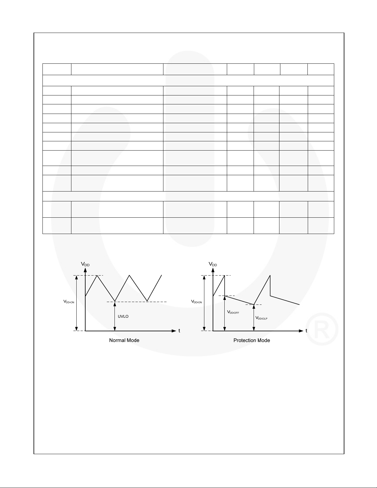
Figure 5. V
Behavior
DD
Continued on the following page…
© 2009 Fairchild Semiconductor Corporation www.fairchildsemi.com
FAN6755W / FAN6755UW • Rev. 1.0.5 6
 Loading...