Fairchild FAN6754WA service manual

FAN6754WA
Highly Integrated Green-Mode PWM Controller
FAN6754WA — Highly Integrated Green-Mode PWM Controller
June 2012
Brownout and V
Adjustment by HV Pin
Limit
Features
High-Voltage Startup
AC Input Brownout Protection with Hysteresis
Monitor HV to Adjust V
Limit
Low Operating Current: 1.5mA
Linearly Decreasing PWM Frequency to 22KHz
Frequency Hopping to Reduce EMI Emission
Fixed PWM Frequency: 65KHz
Peak-Current-Mode Control
Cycle-by-Cycle Current Limiting
Leading-Edge Blanking (LEB)
Internal Open-Loop Protection
GATE Output Maximum Voltage Clamp: 13V
V
V
Under-Voltage Lockout (UVLO)
DD
Over-Voltage Protection (OVP)
DD
Programmable Over-Temperature Protection (OTP)
Internal Latch Circuit (OVP, OTP)
Open-Loop Protection (OLP); Restart for MR, Latch
for ML
SENSE Short-Circuit Protection (SSCP)
Built-in 8ms Soft-Start Function
Applications
General-purpose switch-mode power supplies and
flyback power converters, including:
Power Adapters
Description
The highly integrated FAN6754WA PWM controller
provides several features to enhance the performance
of flyback converters. To minimize standby power
consumption, a proprietary green-mode function
provides off-time modulation to continuously decrease
the switching frequency under light-load conditions.
Under zero-load and very light-load conditions,
FAN6754WA saves PWM pulses by entering "deep"
Burst Mode. This Burst Mode function enables the
power supply to meet international power
conservation requirements.
FAN6754WA also integrates a frequency-hopping
function that helps reduce EMI emission of a power
supply with minimum line filters. The built-in
synchronized slope compensation helps achieve stable
peak-current control. To keep constant output power
limit over universal AC input range, the current limit is
adjusted according to AC line voltage detected by the
HV pin. The gate output is clamped at 13V to protect the
external MOSFET from over-voltage damage.
Other protection functions include AC input brownout
protection with hysteresis, sense pin short-circuit
protection, and V
temperature protection, an external NTC thermistor can
be applied to sense the external switcher’s temperature.
When V
circuit is used to latch-off the controller. The latch mode
is reset when the VDD supply is removed.
FAN6754WA is available in an 8-pin SOP package.
OVP or OTP are activated, an internal latch
DD
over-voltage protection. For over-
DD
Ordering Information
Part Number
FAN6754WAMRMY
FAN6754WAMLMY
© 2011 Fairchild Semiconductor Corporation www.fairchildsemi.com
FAN6754WA • Rev. 1.0.4
Operating
Temperature Range
-40 to +105°C 8-Pin, Small Outline Package (SOP) Tape & Reel
Package Packing Method

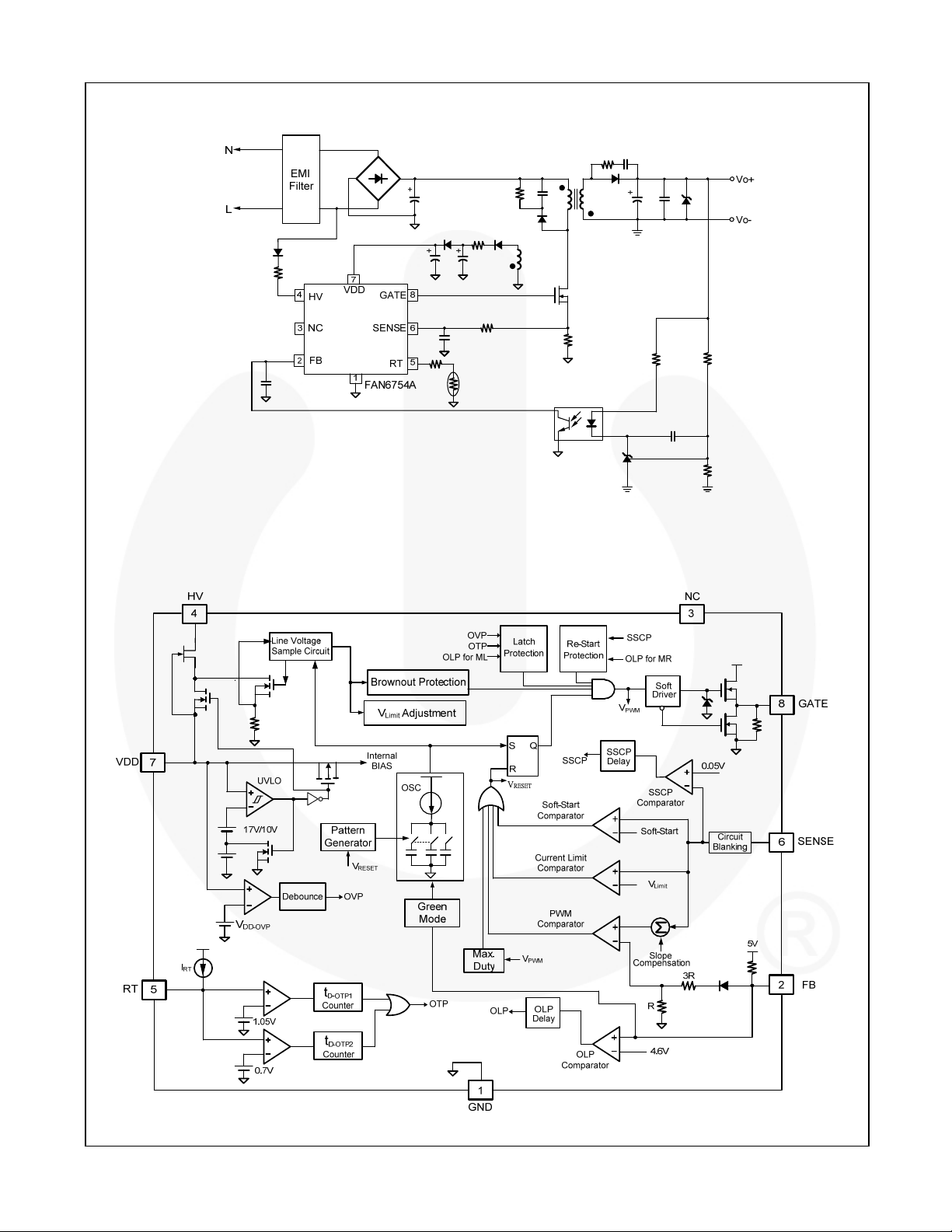
Application Diagram
FAN6754WA — Highly Integrated Green-Mode PWM Controller
Internal Block Diagram
Figure 1. Typical Application
Figure 2. Functional Block Diagram
© 2011 Fairchild Semiconductor Corporation www.fairchildsemi.com
FAN6754WA • Rev. 1.0.4 2

A
A
Marking Information
ZXYTT
6754MR
W
TPM
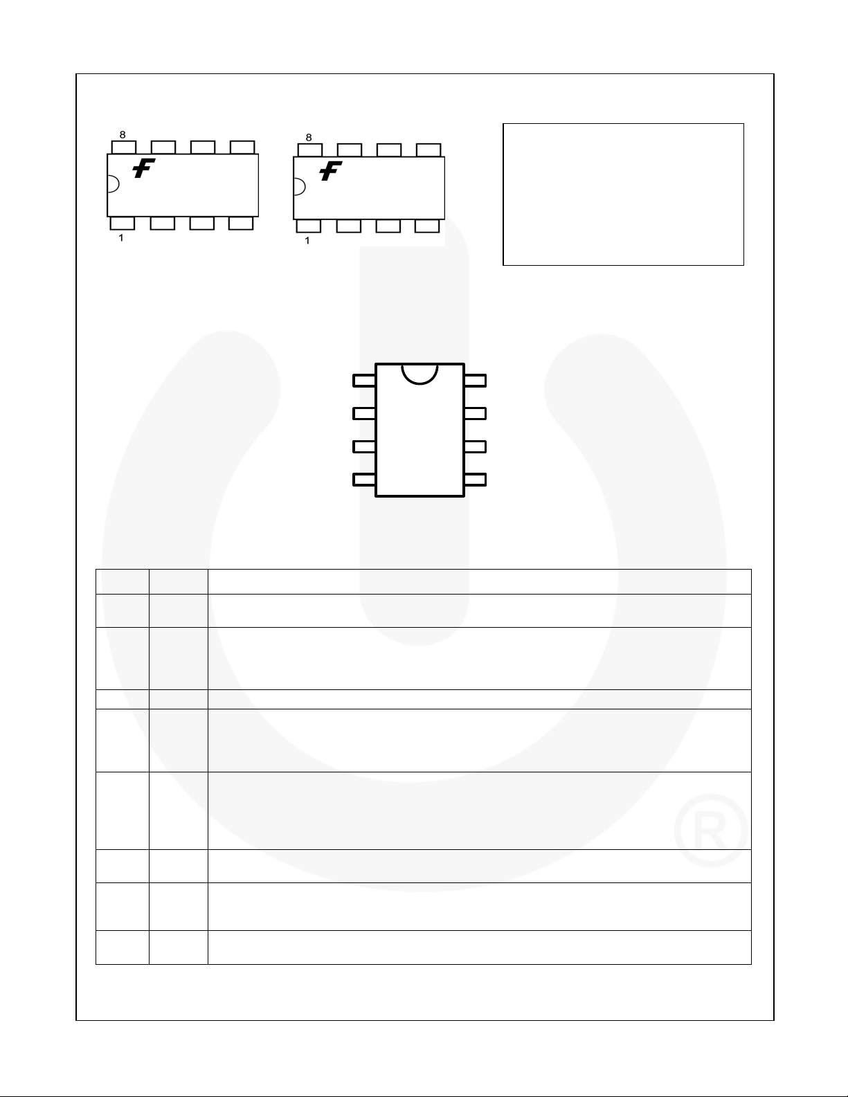
Pin Configuration
ZXYTT
6754ML
W
TPM
Figure 3. Top Mark
SOP-8
FAN6754WA — Highly Integrated Green-Mode PWM Controller
F - Fairchild Logo
Z - Plant Code
X - 1-Digit Year Code
Y - 1-Digit Week Code
TT - 2-Digit Die Run Code
T - Package Type (M=SOP)
P - Y: Package (Green)
M - Manufacture Flow Code
Pin Definitions
Pin # Name Description
1 GND
2 FB
3 NC
4 HV
5 RT
6 SENSE
7 VDD
8 GATE
Ground. This pin is used for the ground potential of all the pins. A 0.1µF decoupling capacitor
placed between VDD and GND is recommended.
Feedback. The output voltage feedback information from the external compensation circuit is fed
into this pin. The PWM duty cycle is determined by this pin and the current-sense signal from Pin
6. FAN6754WA performs open-loop protection (OLP); if the FB voltage is higher than a threshold
voltage (around 4.6V) for more than 56ms, the controller latches off the PWM.
No Connection
High-Voltage Startup. This pin is connected to the line input via a 1N4007 and 200kΩ resistor to
achieve brownout and high/low line compensation. Once the voltage on the HV pin is lower than
the brownout voltage, PWM output turns off. High/low line compensation dominates the cycle-bycycle current limiting to achieve constant output power limiting with universal input.
Over-Temperature Protection. An external NTC thermistor is connected from this pin to GND.
The impedance of the NTC decreases at high temperatures. Once the voltage on the RT pin
drops below the threshold voltage, the controller latches off the PWM. If RT pin is not connected
to NTC resistor for Over-Temperature Protection, a 100KΩ series one resistor is recommended
to ground to prevent from noise interference. This pin is limited by an internal clamping circuit.
Current Sense. This pin is used to sense the MOSFET current for the current-mode PWM and
current limiting.
Supply Voltage. IC operating current and MOSFET driving current are supplied using this pin.
This pin is connected to an external bulk capacitor of typically 47µF. The threshold voltages for
turn-on and turn-off are 17V and 10V, respectively. The operating current is lower than 2mA.
Gate Drive Output. The totem-pole output driver for the power MOSFET. It is internally clamped
below 13V.
GND
FB
NC
HV
Figure 4. Pin Configuration (Top View)
18
2
3
7
6
54
GATE
VDD
SENSE
RT
© 2011 Fairchild Semiconductor Corporation www.fairchildsemi.com
FAN6754WA • Rev. 1.0.4 3

FAN6754WA — Highly Integrated Green-Mode PWM Controller
Absolute Maximum Ratings
Stresses exceeding the absolute maximum ratings may damage the device. The device may not function or be
operable above the recommended operating conditions and stressing the parts to these levels is not recommended.
In addition, extended exposure to stresses above the recommended operating conditions may affect device reliability.
The absolute maximum ratings are stress ratings only.
Symbol Parameter Min. Max. Unit
V
DC Supply Voltage
VDD
VFB FB Pin Input Voltage -0.3 7.0 V
V
SENSE Pin Input Voltage -0.3 7.0 V
SENSE
VRT RT Pin Input Voltage -0.3 7.0 V
VHV HV Pin Input Voltage 500 V
PD
ΘJA
Power Dissipation (T
Thermal Resistance (Junction-to-Air) 150
TJ Operating Junction Temperature -40 +125
T
Storage Temperature Range -55 +150
STG
TL Lead Temperature (Wave Soldering or IR, 10 Seconds) +260
ESD
Electrostatic Discharge Capability,
All Pins Except HV Pin
Notes:
1. All voltage values, except differential voltages, are given with respect to the network ground terminal.
2. Stresses beyond those listed under Absolute Maximum Ratings may cause permanent damage to the device.
3. ESD with HV pin: CDM=1250V and HBM=500V.
(1,2)
30 V
<50°C)
A
400 mW
°C/W
°C
°C
°C
Human Body Model;
JESD22-A114
Charged Device Model;
JESD22-C101
5000
V
2000
Recommended Operating Conditions
The Recommended Operating Conditions table defines the conditions for actual device operation. Recommended
operating conditions are specified to ensure optimal performance to the datasheet specifications. Fairchild does not
recommend exceeding them or designing to Absolute Maximum Ratings.
Symbol Parameter Min. Typ. Max. Unit
TA Operating Ambient Temperature -40 +105 °C
RHV HV Startup Resistor 150 200 250
kΩ
© 2011 Fairchild Semiconductor Corporation www.fairchildsemi.com
FAN6754WA • Rev. 1.0.4 4

FAN6754WA — Highly Integrated Green-Mode PWM Controller
Electrical Characteristics
VDD=15V and TA=25°C unless otherwise noted.
Symbol Parameter Condition Min. Typ. Max. Unit
VDD Section
VOP Continuously Operating Voltage 24 V
V
Start Threshold Voltage 16 17 18 V
DD-ON
V
Minimum Operating Voltage 9 10 11 V
DD-OFF
V
I
DD-OLP
V
DD-LH
V
DD-AC
I
Startup Current V
DD-ST
I
DD-OP1
I
DD-OP2
ILH
I
DD-OLP
V
V
DD-OVP
t
D-VDDOVP
HV Section
Off Voltage 5.5 6.5 7.5 V
DD-OLP
Threshold Voltage on VDD Pin for
Latch-Off Release Voltage
Threshold Voltage on VDD Pin for
Disable AC Recovery to Avoid
Startup Failed
Operating Supply Current,
PWM Operation
Operating Supply Current,
Gate Stop
3.5 4.0 4.5 V
V
– 0.16V 30 µA
DD-ON
=20V, FB=3V Gate
V
DD
DD-OFF
+2.8
Open
V
DD-OFF
+3.3
V
DD-OFF
+3.8
1.5 2.0 mA
VDD=20V, FB=3V 1.0 1.5 mA
Operating Current at PWM-Off
Phase Under Latch-Off
VDD=5V 30 60 90 µA
Conduction
Internal Sink Current Under LatchOff Conduction
Over-Voltage Protection 24 25 26 V
DD
V
Over-Voltage Protection
DD
Debounce Time
V
+0.1V
DD-OLP
75 165 255 µs
170 200 230 µA
V
IHV Supply Current from HV Pin
I
Leakage Current after Startup
HV-LC
VAC=90V(VDC=120V),
=0V
V
DD
HV=700V, VDD=V
+1V
OFF
DD-
DC Source Series
V
Brownout Threshold
AC-OFF
R=200kΩ to HV Pin
See Equation 1
DC Source Series
V
Brownin Threshold
AC-ON
R=200kΩ to HV Pin
See Equation 2
V
ΔVAC
t
Line Voltage Sample Cycle
S-CYCLE
t
Line Voltage Hold Period 20 µs
H-TIME
t
PWM Turn-off Debounce Time
D-AC-OFF
AC-ON
- V
AC-OFF
DC Source Series
R=200kΩ to HV Pin
FB > V
FB < V
FB > V
FB < V
220
FB-N
650
FB-G
65 75 85 ms
FB-N
180 235 290 ms
FB-G
2.0 3.5 5.0 mA
1 20 µA
92 102 112 V
104 114 124 V
6 12 18 V
µs
Continued on the following page…
© 2011 Fairchild Semiconductor Corporation www.fairchildsemi.com
FAN6754WA • Rev. 1.0.4 5
 Loading...