Fairchild FAN6751 service manual

www.fairchildsemi.com
AN-6073
FAN6751 — Highly Integrated Green-Mode PWM Controller
Introduction
This application note describes a detailed design strategy for
a high-efficiency, compact flyback converter. Design
considerations and mathematical equations are presented as
well as guidelines for a printed circuit board layout. The
highly integrated FAN6751 series of PWM controllers
provides several features to enhance the performance for
LCDM/TV, NB, and adapters.
The green-mode function includes off-time modulation and
burst mode to reduce the PWM frequency at light-load and
in no-load conditions. To avoid acoustic noise problems, the
minimum PWM frequency is set above 18KHz. This greenmode function enables the power supply to meet
international power conservation requirements. With the
internal high-voltage startup circuitry, the power loss due to
bleeding resistors is also eliminated. Built-in synchronized
slope compensation achieves stable peak-current-mode
control. The proprietary external line compensation ensures
constant output power limit over a wide AC input voltage
range, from 90V
FAN6751 provides many protection functions, as shown in
Table 1. In addition to cycle-by-cycle current limiting, the
internal open-loop protection circuit ensures safety should
an open-loop or output short-circuit failure occur.
to 264VAC.
AC
Internal Open-loop Protection
GATE Output Maximum Voltage Clamp: 18V
V
V
Under-Voltage Lockout (UVLO)
DD
Over-Voltage Protection (OVP)
DD
Internal Recovery Circuit (OVP, OLP)
Internal Sense Short-Circuit Protection
External Constant Power Limit (Full AC Input Range)
Internal OTP Sensor with Hysteresis
Built-in 5ms Soft-Start Function
Built-in VIN Pin Pull HIGH (> 4.7V) Recovery
Function for Second-Side Output OVP
Brownout Protection with Hysteresis
Applications
General-purpose, switch-mode power supplies and flyback
power converters, including:
Power Adapters
Open-frame SMPS
LCD Monitor/TV
Features
High-Voltage Startup
Low Operating Current: 4mA
Linearly Decreasing PWM Frequency to 18KHz
Fixed PWM Frequency: 65KHz
Peak-Current-Mode Control
Cycle-by-Cycle Current Limiting
Leading-Edge Blanking (LEB)
GND
FB
NC
HV
Figure 1. Pin Configuration (Top View)
SOP-8
1
2
3
4
GATE
8
VDD
7
SENSE
6
VIN
5
Synchronized Slope Compensation
Table 1. Protection Functions of FAN6751 Series
Part Number OVP (VDD) OLP (FB)
FAN6751MRMY Recovery Recovery Recovery Recovery Recovery 65KHz
FAN6751HLMY Latch Latch Latch Recovery Recovery 100KHz
© 2008 Fairchild Semiconductor Corporation www.fairchildsemi.com
Rev. 1.0.0 • 9/26/08
Pull-High
Protection (V
)
IN
OTP
(Internal)
SCP
(SENSE)
PWM
Frequency

AN-6073 APPLICATION NOTE
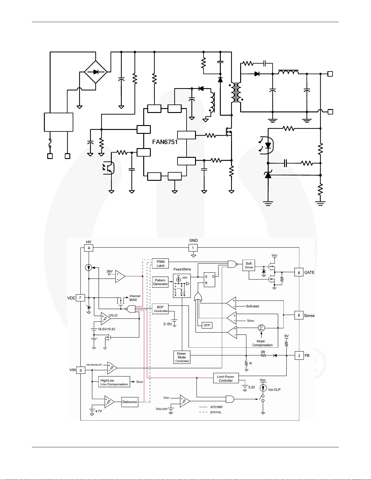
Typical Application
R
C
Sn2
BD1
Sn1
C
Sn1
R
Sn2
L
p
EMI
Filter
Fuse
L
AC
C
2
N
INPUT
Block Diagram
C
Bulk
R
2
R
FB
R
5
2
C
FB
1
VIN
FB
4
HV
NC
R
HV
7
VDD
GATE
SENSE
GND
3
1
C
D1
VDD
8
6
D
Sn
T1
R
g
R
C
LF
Q1
LF
R
S
D2
PC817
KA431
C
O
R
d
C
1
C
V
p
O
R
1
R
3
R
2
Figure 2. Typical Application
Figure 3. Functional Block Diagram
© 2008 Fairchild Semiconductor Corporation www.fairchildsemi.com
Rev. 1.0.0 • 9/26/08 2

AN-6073 APPLICATION NOTE
Internal Block Operation
Startup and Soft-Start Circuitry
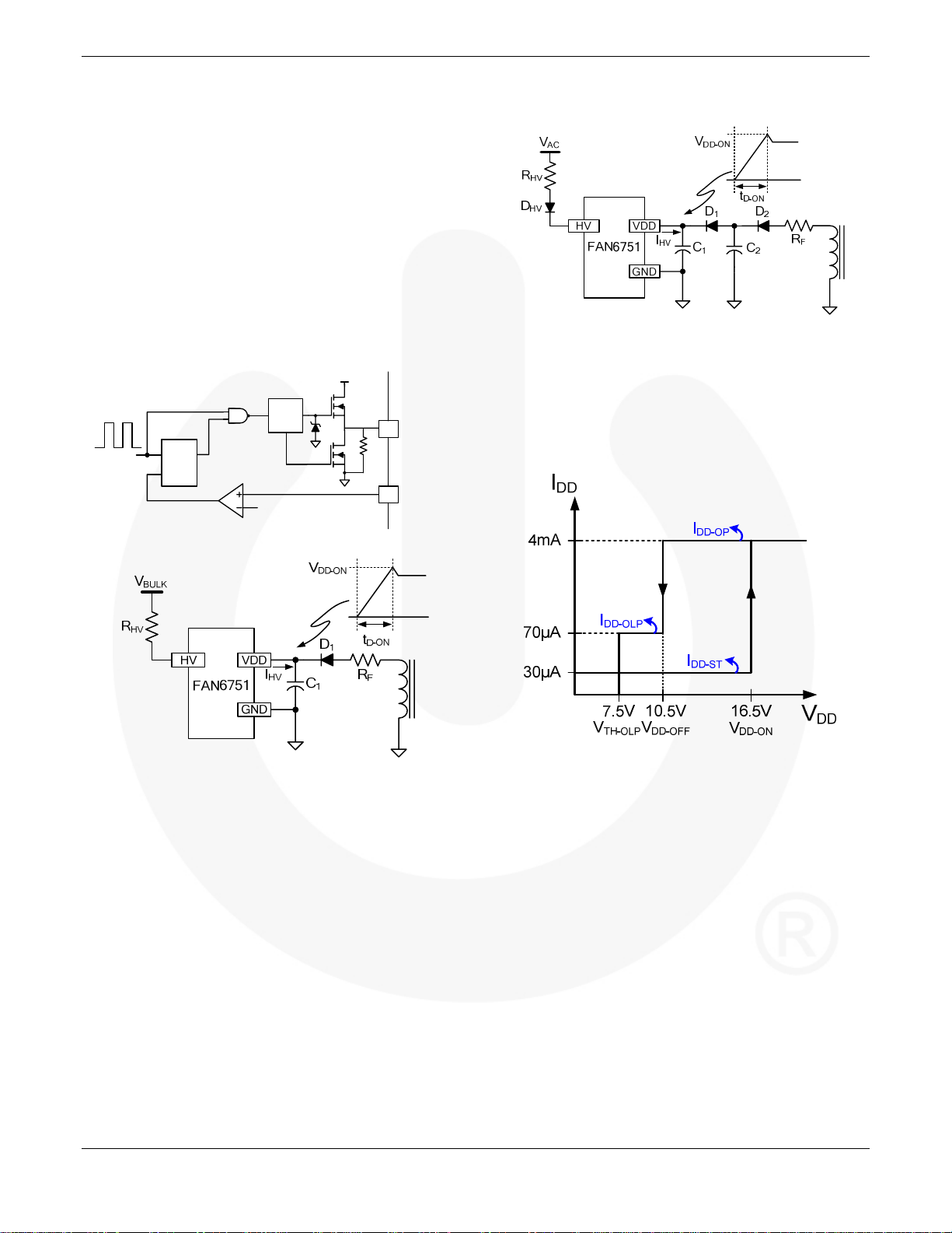
When power is turned on, the internal high-voltage startup
current (typically 2mA) charges the hold-up capacitor C
through startup resistor R
by V
to the HV pin. The built-in 5ms soft-start circuit
BULK
. RHV can be directly connected
HV
starts when the VDD pin reaches the start threshold voltage
V
. Soft-start helps reduce the inrush current, the startup
DD-ON
current spike, and output voltage overshoot during the
startup period, as shown in Figure 4. When V
V
, the internal high-voltage startup current is switched
DD-ON
reaches
DD
off and the supply current is drawn from the auxiliary
winding of the main transformer, as shown in Figure 5.
V
DD
Soft
Driver
S Q
R
Soft Start
GATE
8
6
Sense
1
Figure 6. UVLO Specification
Under-Voltage Lockout (UVLO)
The FAN6751 has a voltage detector on the V
ensure that the chip has enough power to drive the
MOSFET. Figure 7 shows a hysteresis of the turn-on and
turn-off threshold levels and an open-loop-release voltage.
DD
pin to
Figure 4. Soft-start Circuit
Figure 5. Startup Circuit for Power Transfer
If a shorter startup time is required, a two-step startup
circuit, as shown Figure 6, is recommended. In this circuit, a
smaller capacitor C
energy supporting the FAN6751 after startup is mainly from
a larger capacitor C
is required, a D
to the HV pin.
When the supply current is drawn from the transformer, it
draws a leakage current of about 1µA from HV pin. The
maximum power dissipation of the R
2
where
I
is the supply current drawn from HV pin, and
HV-LC
R
is 100KΩ.
HV
can be used to reduce startup time. The
1
. If a shorter releasing latch mode time
2
and RHV can be directly connected by VAC
HV
is:
HV
2
RLIP
×−=
.)(
HVTypCHVRHV
WKAI
μμ
1.0100
≅Ω×=
(1)
Figure 7. UVLO Specification
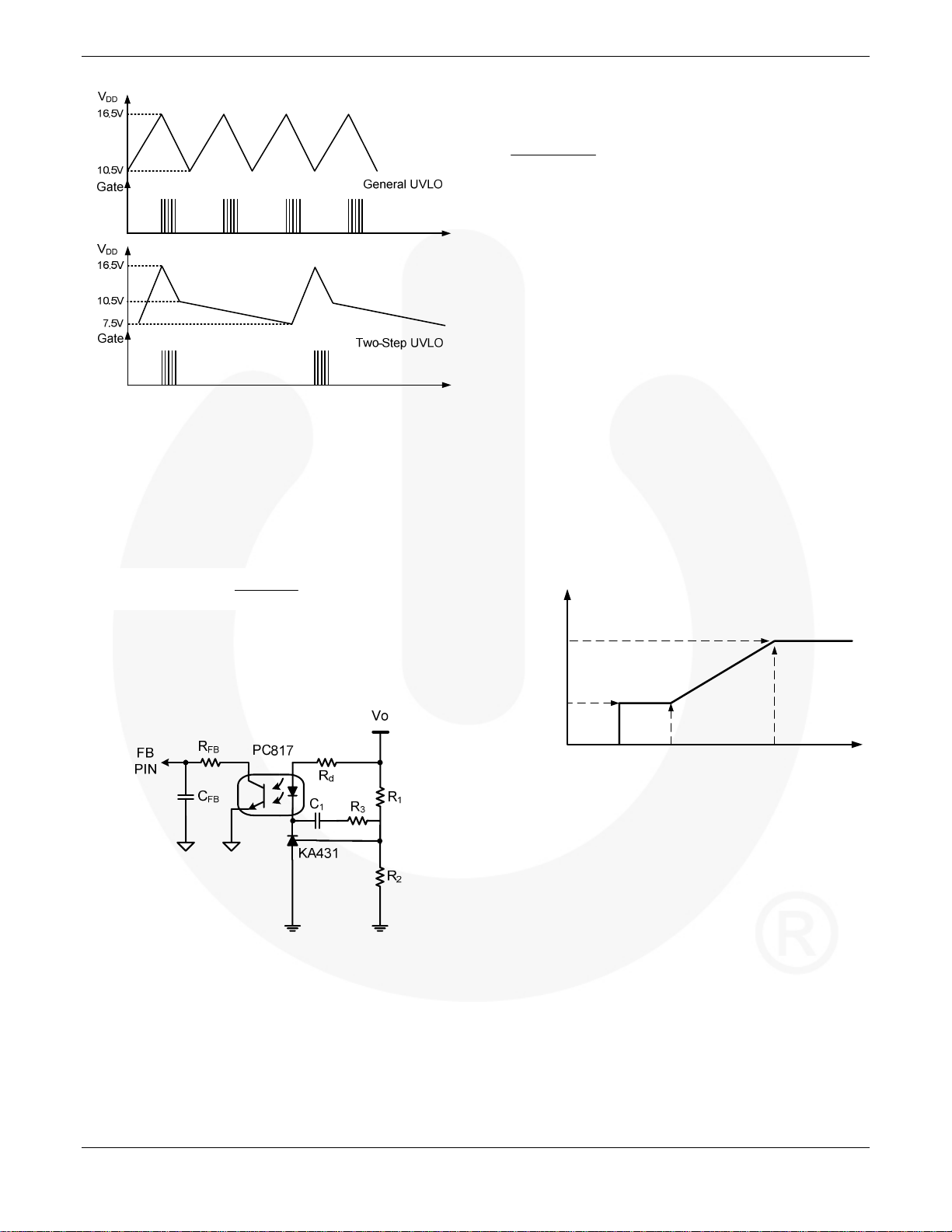
The turn-on and turn-off thresholds are internally fixed at
16.5V and 10.5V. During startup, the V
be charged to 16.5V to enable the IC. The capacitor
continues to supply the V
delivered from the auxiliary winding of the main
transformer. The V
must not drop below 10.5V during the
DD
startup sequence.
To further limit the input power under a short-circuit or
open-loop condition, a special two-step UVLO mechanism
prolongs the discharge time of the V
shows the traditional UVLO method along with the special
two-step UVLO method. In the two-step UVLO mechanism,
an internal sinking current, I
toward the V
V
drops below V
DD
. This sinking current is disabled after the
DD-OLP
DD-OLP
again charged towards V
step UVLO mechanism, the average input power during a
short-circuit or open-loop condition is greatly reduced. As a
’s capacitor must
DD
until the energy can be
DD
capacitor. Figure 8
DD
, pulls the VDD voltage
DD-OLP
; after which, the VDD voltage is
. With the addition of the two-
DD-ON
result, over-heating does not occur.
© 2008 Fairchild Semiconductor Corporation www.fairchildsemi.com
Rev. 1.0.0 • 9/26/08 3

AN-6073 APPLICATION NOTE
Figure 8. UVLO Effect
FB Input
The FAN6751 is designed for peak-current-mode control. A
current-to-voltage conversion is done externally with a
current-sense resistor R
level controls the peak inductor current:
where VFB is the voltage on FB pin and 4 is an internal
divider ratio.
. Under normal operation, the FB
S
V
RIV
=×=
SpkSENSE
FB
6.0−
4
(2)
down at no load. The value of the biasing resistor R
is
b
determined as:
VVV
−−
ZDo
R
b
mAK
5.1≥•
(3)
where:
V
is the drop voltage of photodiode, approximately 1.2V;
D
V
is the minimum operating voltage, 2.5V of the shunt
Z
regulator; and
K is the current transfer rate (CTR) of the opto-coupler.
For an output voltage V
maximum value of R
is 860Ω.
b
=5V with CTR=100%, the
O
Green Mode Operation
Green mode includes off-time modulation and burst mode to
reduce the PWM frequency at light-load and in no-load
conditions. The feedback voltage of the FB pin is taken as a
reference. When the feedback voltage is lower than V
the PWM frequency decreases. Because most losses in a
switching-mode power supply are proportional to the PWM
frequency, the off-time modulation reduces the power
consumption of the power supply at light-load and no-load
conditions. Figure 10 is the PWM frequency is 65KHz at
nominal load and decreases to 18KHz at light load.
Frequency
Fosc:65KHz
PWM Frequency
FB-N
,
When V
is less than 0.6V, the FAN6751 terminates the
FB
output pulses.
Figure 9. Feedback Circuit
Figure 9 is a typical feedback circuit consisting mainly of a
shunt regulator and an opto-coupler. R
voltage divider for the output voltage regulation. R
are adjusted for control-loop compensation. A small-value
RC filter (e.g. R
= 100Ω, CFB= 1nF) placed on the FB pin
FB
to the GND can further increase the stability. The maximum
sourcing current of the FB pin is 1.5mA. The phototransistor
must be capable of sinking this current to pull FB level
and R2 form a
1
and C1
3
Fosc:18KHz
V
FB-ZDC
V
FB-G
V
FB-N
Figure 10. PWM Frequency vs. FB Voltage
The power supply enters “burst mode” in no-load
conditions. As shown in Figure 11 and Figure 12, when V
drops below V
, the PWM output is shuts off and the
FB-ZDC
FB
output voltage drops at a rate dependent on load current.
This causes the feedback voltage to rise. Once V
V
, the internal circuit starts to provide switching pulse.
FB-ZDC
exceeds
FB
The feedback voltage then falls and the process repeats.
Burst mode operation alternately enables and disables
switching of the MOSFET, reducing the switching losses in
standby mode.
© 2008 Fairchild Semiconductor Corporation www.fairchildsemi.com
Rev. 1.0.0 • 9/26/08 4
 Loading...