Fairchild FAN6749 service manual

May 2012
FAN6749
Highly Integrated Ultra Green-Mode PWM Controller
FAN6749 — Highly Integrated Ultra Green-Mode PWM Controller
Features
High-Voltage Startup
Low Operating Current: 1.8mA
Linearly Decreasing PWM Frequency to 24kHz
Proprietary Frequency Hopping to Reduce EMI
Two-Level Over-Current Protection (OCP),
1400ms Delay for Normal Peak Load
Two-Level OCP, 56ms Delay for Super Peak Load
Output Short-Circuit Protection (SCP)
Peak-Current Mode Operation with Cycle-by-Cycle
Current Limiting
HV Pin Brown-in/out Protection with Hysteresis
Constant Power Limit by HV Sampling
Internal FB Open-Loop Protection (OLP)
GATE Output Maximum Voltage Clamp: 14.5V
V
Over-Voltage Protection (OVP)
DD
Programmable Over-Temperature Protection (OTP)
Integrated 6ms Soft-Start Function
Internal Latch Circuit (OVP, OTP, OCP, OLP, SCP)
Internal OTP Sensor with Hysteresis
Applications
General-Purpose Switched-Mode Power Supplies and
Flyback Power Converters, including:
Power Adapters
Open-Frame SMPS; Specifically for SMPS with
Surge-Current Output, such as for Printer, Scanner,
Motor Drivers
Description
The FAN6749 highly integrated PWM controller
enhances the performance of flyback converters. To
minimize standby power consumption, a proprietary
Green-Mode function continuously decreases the
switching frequency under light-load conditions. Under
zero-load conditions, the power supply enters Burst
Mode and completely shuts off PWM output. Green
Mode helps power supplies meet international power
conservation requirements.
The FAN6749 is designed for SMPS with surge-current
output and incorporates a two-level Over-Current
Protection (OCP) function. Besides the cycle-by-cycle
current limiting, two-level OCP can handle peak loading
within a specified delay time.
FAN6749 also integrates a frequency-hopping function
that helps reduce EMI emission of a power supply with
minimum line filters. Built-in synchronized slope
compensation helps achieve stable peak-current control.
To keep constant output power limit over universal AC
input range, the current limit and OCP threshold voltage
are adjusted according to AC line voltage detected by
the HV pin. Gate output is clamped at 14.5V to protect
the external MOSFET from over-voltage damage.
Other protection functions include: AC input brownout
protection with hysteresis, Short-Circuit Protection
(SCP) for output-short condition, and V
Protection (OVP). For over-temperature protection, an
external NTC thermistor can be applied to sense the
ambient temperature. When OLP, OCP, SCP, V
or OTP is activated, an internal latch circuit latches off
the controller. The latch resets when V
OVP OCP OLP OTP SCP
Latch Latch Latch Latch Latch
There are three differences from FAN6748 to FAN6749:
Over-Voltage
DD
is removed.
DD
OVP,
DD
Over-current protection debounce time is extended
to 1400ms.
Brown-out debounce time is extended to 100ms.
No SENSE short-circuit protection function.
Ordering Information
Part Number Operating Temperature Range Package
FAN6749MLM -40 to +105°C 8-Pin Small Outline Package (SOP) Reel & Tape
© 2012 Fairchild Semiconductor Corporation www.fairchildsemi.com
FAN6749 • Rev. 1.0.1
Packing
Method

Application Diagram
FAN6749 — Highly Integrated Ultra Green-Mode PWM Controller
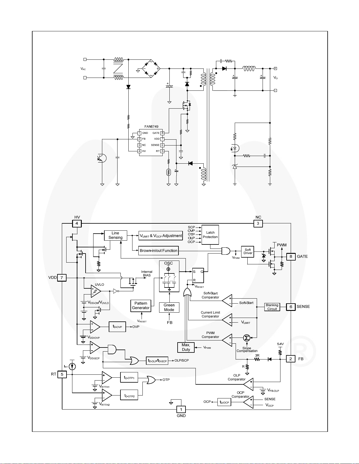
Figure 1. Typical Application
Internal Block Diagram
Figure 2. Functional Block Diagram
© 2012 Fairchild Semiconductor Corporation www.fairchildsemi.com
FAN6749 • Rev. 1.0.1 2

Marking Information
Pin Configuration
ZXYTT
6749ML
TM
F - Fairchild Logo
Z - Plant Code
X - 1-Digit Year Code
Y - 1-Digit Week Code
TT - 2-Digit Die Run Code
T - Package Type (M=SOP)
M - Manufacture Flow Code
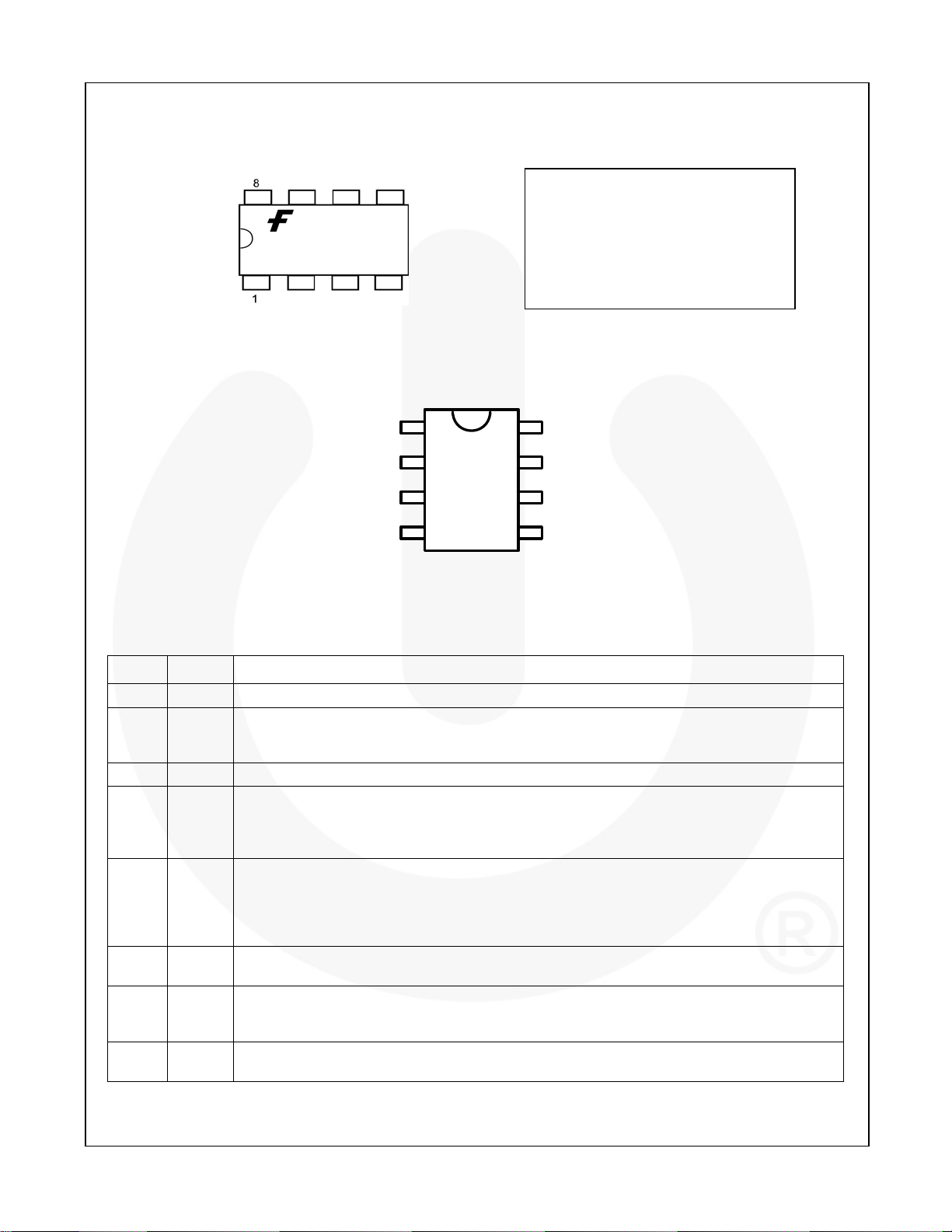
Figure 3. Top Mark
FAN6749 — Highly Integrated Ultra Green-Mode PWM Controller
Pin Definitions
Pin # Name Description
1 GND
2 FB
3 NC No Connection
4 HV
5 RT
6 SENSE
7 VDD
8 GATE
Ground Pin. A 0.1µF decoupling capacitor between VDD and GND is recommended.
Feedback Pin. The output voltage feedback information from the external compensation circuit is
fed into this pin. The PWM duty cycle is determined by comparing the FB signal with currentsense signal from the SENSE pin.
High-Voltage Startup. The HV pin is typically connected to the AC line input through an external
diode and a resistor (R
also to sense the line voltage. The line voltage information is used for brown-out protection and
power limit line compensation.
Over-Temperature Protection. An external NTC thermistor is connected from this pin to the
GND pin. Once the voltage of the RT pin drops below the threshold voltage, the controller latches
off the PWM. The RT pin also provides external latch protection. If the RT pin is not connected to
an NTC resistor for over-temperature protection, place a 100k resistor to ground to prevent
noise interference.
Current Sense. The sensed voltage is used for peak-current-mode control, over-current
protection, short-circuit protection, and cycle-by-cycle current limiting.
Power Supply of IC. A holdup capacitor typically connects from this pin to ground. A rectifier
diode in series with the transformer auxiliary winding connects to this pin to supply bias during
normal operation.
Gate Drive Output. The totem-pole output driver for the power MOSFET; internally limited to
V
GATE-CLAMP
.
GND
FB
NC
HV
Figure 4. Pin Configuration (Top View)
HV
18
2
3
7
6
54
). This pin is used not only to charge VDD capacitor during startup, but
GATE
VDD
SENSE
RT
© 2012 Fairchild Semiconductor Corporation www.fairchildsemi.com
FAN6749 • Rev. 1.0.1 3

FAN6749 — Highly Integrated Ultra Green-Mode PWM Controller
Absolute Maximum Ratings
Stresses exceeding the absolute maximum ratings may damage the device. The device may not function or be
operable above the recommended operating conditions and stressing the parts to these levels is not recommended.
In addition, extended exposure to stresses above the recommended operating conditions may affect device reliability.
The absolute maximum ratings are stress ratings only.
Symbol Parameter Min. Max. Unit
VDD DC Supply Voltage
VFB FB Pin Input Voltage -0.3 7.0 V
V
SENSE Pin Input Voltage -0.3 7.0 V
SENSE
VRT RT Pin Input Voltage -0.3 7.0 V
VHV HV Pin Input Voltage 500 V
PD
JA
Power Dissipation (T
Thermal Resistance (Junction-to-Air) 150
TJ Operating Junction Temperature -40 +125
T
Storage Temperature Range -55 +150
STG
TL Lead Temperature (Wave Soldering or IR, 10 Seconds) +260
ESD
Human Body Model
Charged Device Model
Notes:
1. All voltage values, except differential voltages, are given with respect to the network ground terminal.
2. Stresses beyond those listed under “absolute maximum ratings” may cause permanent damage to the device.
3. ESD with the HV pin CDM=1000V and HBM=500V.
(1,2)
30 V
<50°C)
A
400 mW
C/W
C
C
C
(3)
, JEDEC:JESD22-A114 All Pins Except HV Pin 6 kV
(3)
, JEDEC:JESD22-C101 All Pins Except HV Pin 2 kV
Recommended Operating Conditions
The Recommended Operating Conditions table defines the conditions for actual device operation. Recommended
operating conditions are specified to ensure optimal performance to the datasheet specifications. Fairchild does not
recommend exceeding them or designing to Absolute Maximum Ratings.
Symbol Parameter Min. Typ. Max. Unit
RHV HV Startup Resistor 150 200 250 k
© 2012 Fairchild Semiconductor Corporation www.fairchildsemi.com
FAN6749 • Rev. 1.0.1 4

Electrical Characteristics
VDD=15V and TA=25C unless otherwise noted.
Symbol Parameter Conditions Min. Typ. Max. Unit
VDD Section
VOP Continuously Operating Voltage Limited by VDD OVP 25 V
V
Threshold Voltage to Startup VDD Rising 16 17 18 V
DD-ON
V
DD-OFF
V
DD-OLP
V
UVLO
V
RESTART
V
DD-LH
V
DD-AC
V
DD-SCP
t
D-SCP
I
DD-ST
I
DD-OP1
I
DD-OP2
ILH
I
DD-OLP
V
DD-OVP
t
D-VDDOVP
Threshold Voltage to Stop
Switching in Protection Mode
Threshold Voltage to Turn On HV
Startup in Protection Mode
Threshold Voltage to Stop
Switching in Normal Mode
VDD Falling
VDD Falling 6.5 7.5 8.5 V
VDD Falling 6.0 6.5 7.0 V
Threshold Voltage to Enable HV
Startup to Charge VDD in Normal
VDD Falling 4.5 5.0 5.5 V
Mode
Threshold Voltage to Release
Latch Mode
VDD Falling 3.5 4.0 4.5 V
Threshold Voltage on VDD Pin for
Disable Brown-in to Avoid Startup
Failure
Threshold Voltage on VDD Pin for
Short-Circuit Protection (SCP)
Debounce Time for SCP
Startup Current V
Supply Current in PWM Operation
V
> V
FB
V
FB>VFB-OLP
& V
DD
DD-ON
=20V, VFB = 3V Gate
V
DD
FB-OLP
< V
DD-SCP
– 0.16V 30 µA
Open
Supply Current when PWM Stops VDD=15V, VFB < 1.4V 1.0 1.9 mA
Operating Current when V
in Protection Mode
OFF
Internal Sink Current
Threshold Voltage for V
Voltage Protection
Over-Voltage Protection
V
DD
Debounce Time
DD<VDD-
Over-
DD
VDD = 5V 100 120 140 µA
V
+0.1V
DD-OLP
28.5 29.0 29.9 V
160 200 240 µs
10 11 12
V
UVLO
+2.5
V
DD-OFF
+1.0
V
V
UVLO
+3 V
DD-OFF
+1.5
+3.5 V
UVLO
V
+2.0 V
DD-OFF
V
12 17 22 ms
1.8 2.4 mA
265 325 385 µA
FAN6749 — Highly Integrated Ultra Green-Mode PWM Controller
V
DD
V
DD-ON
GATE
V
UVLO
Normal Mode
V
RESTART
t
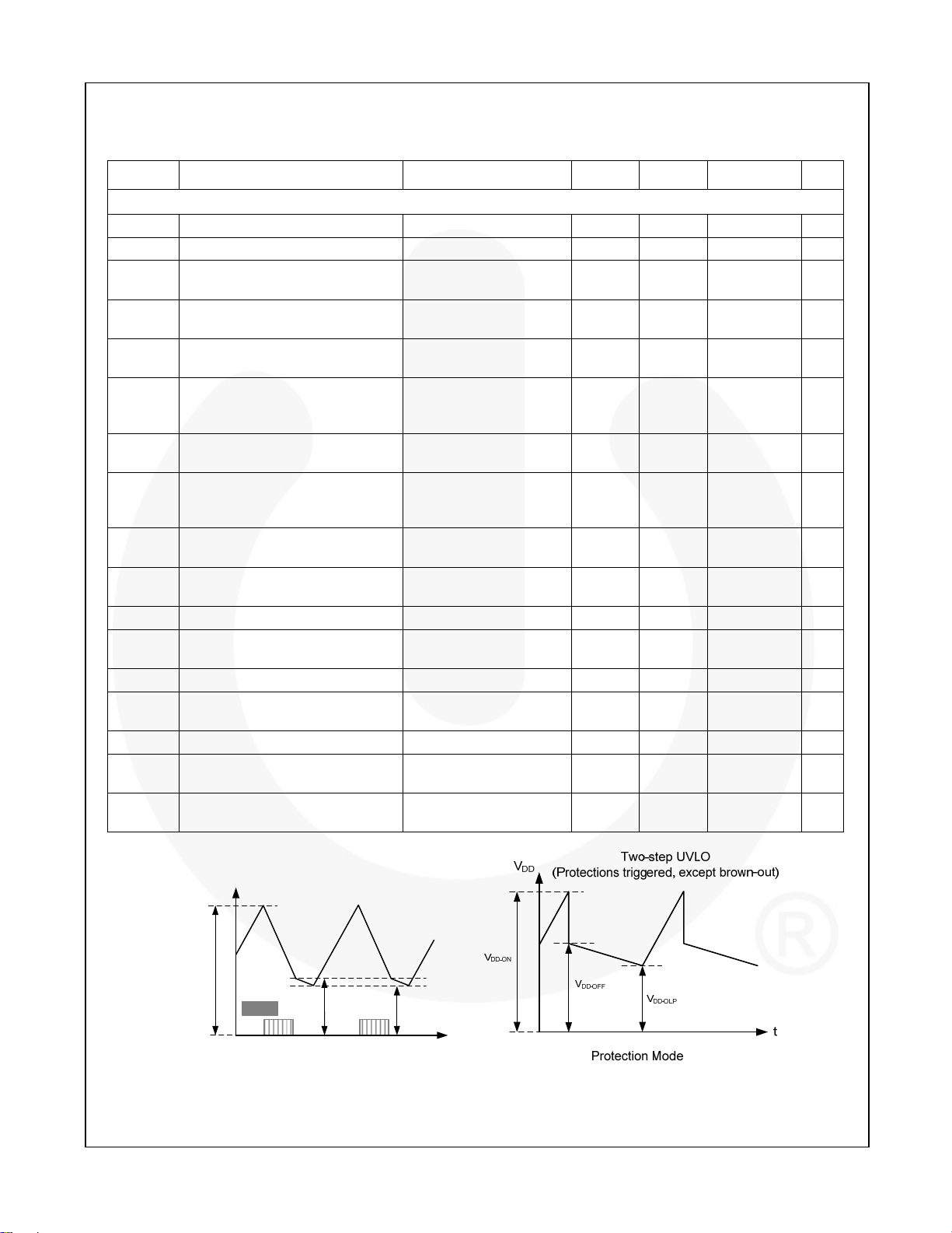
Figure 5. VDD Behavior
© 2012 Fairchild Semiconductor Corporation www.fairchildsemi.com
FAN6749 • Rev. 1.0.1 5
Continued on the following page…
 Loading...