Fairchild FAN6747WL service manual

FAN6747WL
Highly Integrated Green-Mode PWM Controller
FAN6747WL — Highly Integrated Green-Mode PWM Controller
May 2012
Features
High-Voltage Startup
AC-Line Brownout Protection by HV Pin
Constant Output Power Limit by HV Pin
(Full AC-Line Range)
Built-in 8ms Soft-Start Function
Two-Level Over-Current Protection (OCP) with
215ms Debounce
Short-Circuit Protection (SCP) with 15ms Debounce
as Output Short
Peak-Current Mode Operation with Cycle-by-Cycle
Current Limiting
Low Startup Current: 30µA
Low Operating Current: 1.7mA
Over-Temperature Protection (OTP) with External
Negative-Temperature-Coefficient (NTC) Thermistor
PWM Frequency Decreasing at Green-Mode
V
Over-Voltage Protection (OVP)
DD
Internal Latch Circuit for OVP, OTP, SCP, and OCP
Applications
General-purpose switch-mode power supplies and
flyback power converters, including:
Power Adapters
SMPS with Peak-Current Output, such as for
Printers, Scanners, Motor Drivers
AC/DC NB Adapters
Open-Frame SMPS
Description
The highly integrated FAN6747WL PWM controller
provides several features to enhance the performance
of flyback converters. To minimize standby power
consumption, a proprietary Green-Mode function
provides off-time modulation to decrease the switching
frequency with load condition.
Under zero-load condition, the power supply enters
Burst Mode and burst frequency can be low to reduce
power. Green Mode enables the power supply to meet
international power conservation requirements.
The FAN6747WL is specially designed for SMPS with
peak-current output. It incorporates a cycle-by-cycle
current limiting and two-level Over-Current-Protection
(OCP) that can handle peak load with a debounce time.
Once the current is over the threshold level, it triggers
the first counter 15ms and checks if V
it is, the PWM latches off for SCP. If V
10V; it keeps counting to 215ms, then the PWM latches
off for OCP.
FAN6747WL also integrates a frequency-hopping
function that helps reduce EMI emission of a power
supply with minimum line filters. The built-in
synchronized slope compensation helps achieve stable
peak-current control. To keep constant output power
limit over universal AC input range, the current limit and
OCP threshold voltage are adjusted according to AC
line voltage detected by the HV pin. The gate output is
clamped at 13.5V to protect the external MOSFET from
over-voltage damage.
Other protection functions include AC-line brownout
protection with hysteresis and V
protection. For over-temperature protection, an external
NTC thermistor is applied to sense the ambient
temperature. When OCP, OVP, SCP, or OTP is
activated, an internal circuit latches off the controller.
The latch is reset when V
drops to V
DD
is below 10V; if
DD
is higher than
DD
over-voltage
DD
.
DD-LH
Ordering Information
Part Number
FAN6747WLMY -40 to +105°C
© 2012 Fairchild Semiconductor Corporation www.fairchildsemi.com
FAN6747WL • Rev. 1.0.1
Operating
Temperature Range
Package Packing Method
8-Lead, Small-Outline Integrated Circuit (SOIC),
JEDEC MS-012, .15-Inch Narrow Body
Tape & Reel

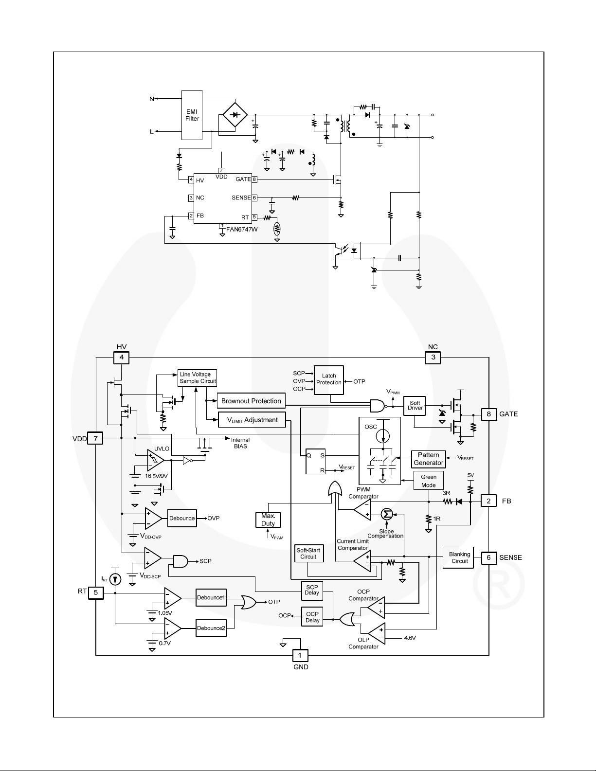
Application Diagram
FAN6747WL — Highly Integrated Green-Mode PWM Controller
Figure 1. Typical Application
Internal Block Diagram
Figure 2. Functional Block Diagram
© 2012 Fairchild Semiconductor Corporation www.fairchildsemi.com
FAN6747WL • Rev. 1.0.1 2

Marking Information
ZXYTT
6747F
WTPM
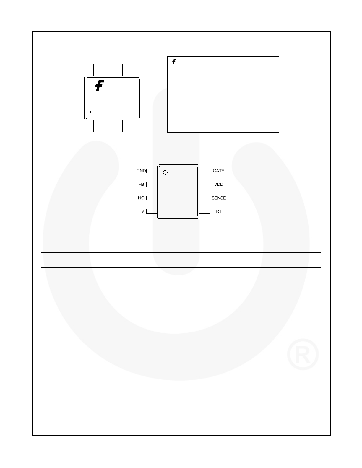
Pin Configuration
: Fairchild Logo
Z: Plant Code
X: Year Code
Y: Week Code
TT: Die Run Code
F: L = OCP latch
T: Package Type (N = DIP, M = SOP)
P: Y = Green Compound
M: Manufacturing Flow Code
Figure 3. Top Mark
FAN6747WL — Highly Integrated Green-Mode PWM Controller
Figure 4. Pin Assignments
Pin Definitions
Pin # Name Description
1 GND
2 FB
3 NC No Connection
4 HV
5 RT
6 SENSE
7 VDD
8 GATE
Ground. This pin is used for the ground potential of all the pins. A 0.1µF decoupling capacitor
placed between VDD and GND is recommended.
Feedback. The output voltage feedback information from the external compensation circuit is fed
into this pin. The PWM duty cycle is determined from this pin and the current-sense signal from
Pin 6.
High-Voltage Startup. This pin is connected to the line input via diodes and resistors to meet
brownout and high/low line compensation. Once the voltage of the HV pin is lower than the
brownout voltage, PWM output is turned off. High/low line compensation dominates the OCP
level and cycle-by-cycle current limit to solve the unequal OCP level and power-limit problems
under universal input.
Over-Temperature Protection. For over-temperature protection, an external NTC thermistor is
connected from this pin to GND. The impedance of the NTC decreases at high temperatures.
Once the voltage of the RT pin drops below the threshold voltage, the controller latches off the
PWM. If the RT pin is not connected to the NTC resistor for over temperature protection, it is
recommended to connect one 100KΩ resistor to ground to prevent noise interference. This pin is
limited by internal clamping circuit.
Current Sense. This pin is used to sense the MOSFET current for the Current-Mode PWM and
OCP. If the switching current is higher than the OCP threshold and lasts 215ms, the controller
latches off the PWM.
Supply Voltage. IC operating current and MOSFET driving current are supplied using this pin.
This pin is connected to an external bulk capacitor of typically 10µF. The threshold voltages for
startup and turn-off are 16.5V and 9V, respectively. The operating current is lower than 2mA.
Gate Driver Output. The totem-pole output driver for the power MOSFET. It is internally
clamped below 13.5V.
© 2012 Fairchild Semiconductor Corporation www.fairchildsemi.com
FAN6747WL • Rev. 1.0.1 3

FAN6747WL — Highly Integrated Green-Mode PWM Controller
Absolute Maximum Ratings
Stresses exceeding the absolute maximum ratings may damage the device. The device may not function or be
operable above the recommended operating conditions and stressing the parts to these levels is not recommended.
In addition, extended exposure to stresses above the recommended operating conditions may affect device reliability.
The absolute maximum ratings are stress ratings only.
Symbol Parameter Min. Max. Unit
VDD DC Supply Voltage 30 V
VHV
VL Input Voltage to FB, SENSE, RT Pin -0.3 7.0 V
PD Power Dissipation (TA<50°C) 400 mW
ΘJA
TJ Operating Junction Temperature -40 +125 °C
T
TL Lead Temperature (Soldering, 10 Seconds) +260 °C
ESD
Notes:
1. Stresses beyond those listed under Absolute Maximum Ratings may cause permanent damage to the device.
2. All voltage values, except differential voltages, are given with respect to the network ground terminal.
3. ESD with the HV pin: CDM = 1250V and HBM = 1000V.
Suddenly Input Voltage to HV Pin within 1 Second
(Series connect with R
Thermal Resistance (Junction-to-Ambient) 150 °C/W
Storage Temperature Range -55 +150 °C
STG
Electrostatic Discharge Capability,
All Pins Except HV Pin
HV
(3)
)
Human Body Model, JESD22-A114 5
Charge Device Model, JESD22-C101 2
640 V
kV
Recommended Operating Conditions
The Recommended Operating Conditions table defines the conditions for actual device operation. Recommended
operating conditions are specified to ensure optimal performance to the datasheet specifications. Fairchild does not
recommend exceeding them or designing to Absolute Maximum Ratings.
Symbol Parameter Min. Typ. Max. Unit
TA Operating Ambient Temperature -40 +105 °C
VHV Input Voltage to HV Pin 500 V
RHV HV Startup Resistor 150 200 250 k
© 2012 Fairchild Semiconductor Corporation www.fairchildsemi.com
FAN6747WL • Rev. 1.0.1 4

Electrical Characteristics
VDD = 15V and TA = 25°C, unless otherwise specified.
Symbol Parameter Condition Min. Typ. Max. Unit
VDD Section
VOP Continuously Operating Voltage 24 V
V
Turn-On Threshold Voltage 15.5 16.5 17.5 V
DD-ON
V
PWM Turn-Off Threshold Voltage 8 9 10 V
DD-OFF
Threshold Voltage on VDD for HV
V
DD-OLP
JFET Turn-On in Protection
Condition
V
DD-LH
Threshold Voltage on VDD Pin for
Latch-Off Release Voltage
Threshold Voltage on VDD Pin for
V
DD-AC
Disable AC Recovery to Avoid
Startup Failure
V
DD-SCP
ILH
I
DD-ST
I
DD-OLP
I
DD-OP1
I
DD-OP2
Threshold Voltage on VDD Pin for
Short-Circuit Protection (SCP)
Holding Current Under Latch-Off
Condition
Startup Current V
Holding Current at PWM-Off
Phase
Operating Supply Current when
PWM Operating
Operating Supply Current when
PWM Stopped
Threshold Voltage on VDD Pin for
V
DD-OVP
VDD Over-Voltage Protection
(Latch-Off)
t
D-OVP
VDD OVP Debounce Time VFB > V
After Trigger OCP/
SCP/ OVP/ OTP
5.5 6.5 7.5 V
3.5 4.0 4.5 V
V
> V
FB
FBO
V
= 5V 80 100 120 A
DD
– 0.16V 30 A
DD-ON
V
V
+ 0.1V 180 240 300 A
DD-OLP
= 20V, V
DD
FB
= 3V,
V
V
Gate Open
VDD = 20V, V
FB
= 3V,
Gate Open
DD-OFF
DD-OFF
+2.5 V
+0.5 V
DD-OFF
DD-OFF
+3.0 V
+1.0 V
DD-OFF
DD-OFF
+3.5 V
+1.5 V
1.7 2.0 mA
1.2 1.5 mA
24 25 26 V
75 160 245 s
FB-N
Continued on the following page…
FAN6747WL — Highly Integrated Green-Mode PWM Controller
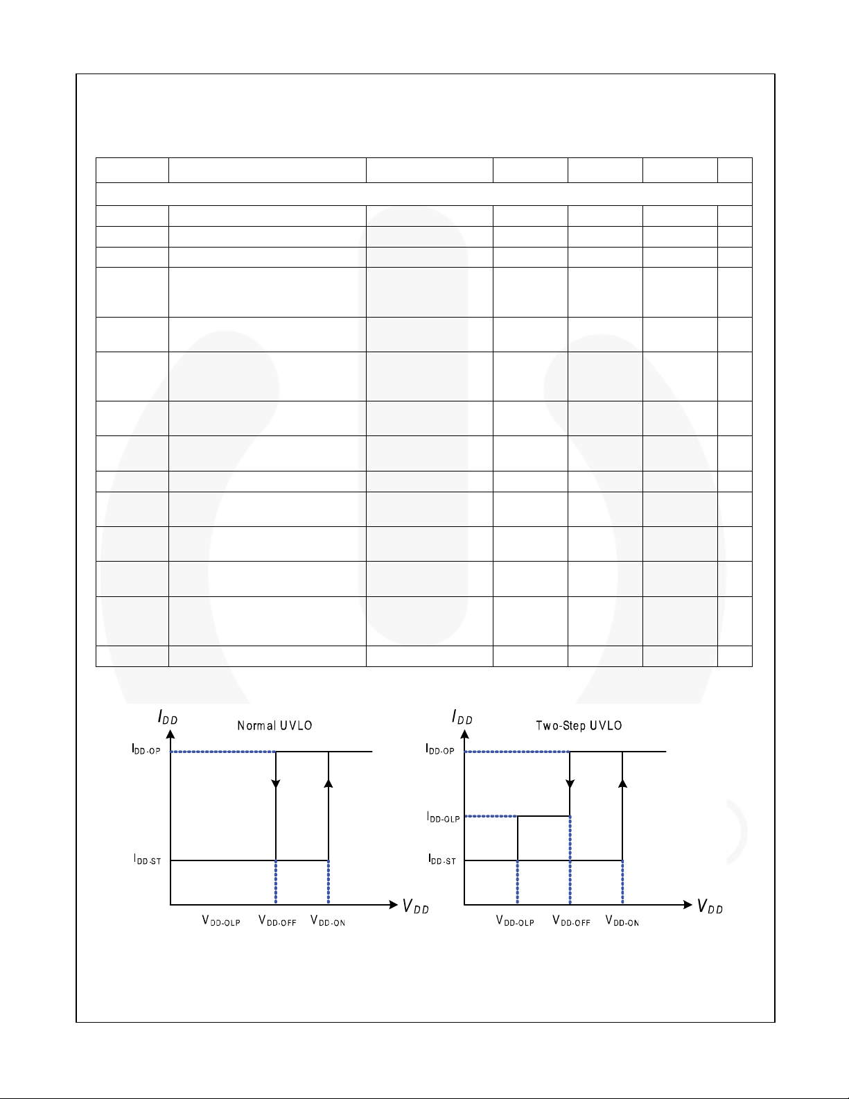
Figure 5. UVLO Specification
© 2012 Fairchild Semiconductor Corporation www.fairchildsemi.com
FAN6747WL • Rev. 1.0.1 5
 Loading...