Fairchild FAN6300A, FAN6300H service manual

December 2009
FAN6300A / FAN6300H
Highly Integrated Quasi-Resonant Current Mode
PWM Controller
FAN6300A/H — Highly Integrated Quasi-Resonant Current Mode PWM Controller
Features
High-Voltage Startup
Quasi-Resonant Operation
Cycle-by-Cycle Current Limiting
Peak-Current-Mode Control
Leading-Edge Blanking (LEB)
Internal Minimum t
OFF
Internal 5ms Soft-Start
Over Power Compensation
GATE Output Maximum Voltage
Auto-Recovery Over-Current Protection(FB Pin)
Auto-Recovery Open-Loop Protection(FB Pin)
VDD Pin and Output Voltage (DET Pin)
OVP Latched
Low Frequency Operation (below 100kHz) for
FAN6300A
High Frequency Operation (up to 190kHz) for
FAN6300H
Applications
AC/DC NB Adapters
Open-Frame SMPS
Description
The highly integrated FAN6300A/H of PWM controller
provides several features to enhance the performance
of flyback converters. FAN6300A is applied on quasiresonant flyback converters where maximum operating
frequency is below 100kHz. FAN6300H is suitable for
high-frequency operation (up to 190kHz). A built-in HV
startup circuit can provide more startup current to
reduce the startup time of the controller. Once the V
voltage exceeds the turn-on threshold voltage, the HV
startup function is disabled immediately to reduce
power consumption. An internal valley voltage detector
ensures power system operates at quasi-resonant
operation over a wide-range of line voltage and any
load conditions, as well as reducing switching loss to
minimize switching voltage on drain of power MOSFET.
To minimize standby power consumption and light-load
efficiency, a proprietary green-mode function provides
off-time modulation to decrease switching frequency
and perform extended valley voltage switching to keep
to a minimum switching voltage. The operating
frequency is limited by minimum t
to 8µs in FAN6300A and 13µs to 3µs in FAN6300H, so
FAN6300H can operate at higher switching frequency
than FAN6300A.
FAN6300A/H controller also provides many protection
functions. Pulse-by-pulse current limiting ensures the
fixed-peak current limit level, even when a short circuit
occurs. Once an open-circuit failure occurs in the
feedback loop, the internal protection circuit disables
PWM output immediately. As long as V
the turn-off threshold voltage, the controller also
disables PWM output. The gate output is clamped at
18V to protect the power MOS from high gate-source
voltage conditions. The minimum t
prevents the system frequency from being too high. If
the DET pin triggers OVP, internal OTP is triggered and
the power system enters latch-mode until AC power is
removed.
The FAN6300A/H controller is available in the 8-pin
Small Outline Package (SOP) and the Dual Inline
Package (DIP).
time, which is 38µs
off
drops below
DD
time limit
OFF
DD
© 2009 Fairchild Semiconductor Corporation www.fairchildsemi.com
FAN6300A/H • Rev. 1.0.1

Ordering Information
FAN6300A/H — Highly-Integrated Quasi-Resonant Current Mode PWM Controller
Part Number
FAN6300AMY Green -40°C to +125°C 8-Lead, Small Outline Package (SOP) Tape & Reel
FAN6300HMY Green -40°C to +125°C 8-Lead, Small Outline Package (SOP) Tape & Reel
FAN6300ANY Green -40°C to +125°C 8-Lead, Dual In-line Package (DIP) Tube
FAN6300HNY Green -40°C to +125°C 8-Lead, Dual In-line Package (DIP) Tube
For Fairchild’s definition of Eco Status, please vis it: http://www.fairchildsemi.com/company/green/rohs_green.html
Eco Status
Operating
Temperature Range
Package
Packing
Method
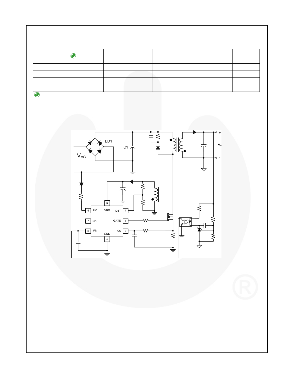
Application Diagram
Figure 1. Typical Application
© 2009 Fairchild Semiconductor Corporation www.fairchildsemi.com
FAN6300A(H) Rev. 1.0.1 2

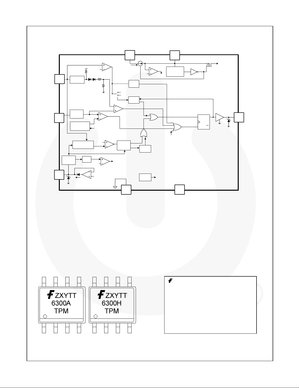
Internal Block Diagram
FAN6300A/H — Highly Integrated Quasi-Resonant Current Mode PWM Controller
FB
CS
DET
HV
8
27 V
FB OLP
t
TIME -OUT
Intern a l
OTP
OVP
I
2.1ms
30 µs
Valley
Detector
HV
Timer
52m s
Starter
4.2V
S/H
2R
I
DET
0.3V
V
DET
V
DET
2.5V
0.3V
R
PW M
Current Lim it
DET OVP
Latched
Soft -S tar t
2
3
1
t
OFF
Blanking
5ms
Blanking
Circuit
Over-Power
Com pensation
I
5V
t
OFF-MIN
DET
Latched
Latched
VDD
6
Two Steps
UVLO
16 V /10 V / 8V
Latched
Intern al
Bias
SET
S
R
CLR
DRV
Q
Q
18V
5
GATE
Marking Information
4 7
GND
Figure 2. Functional Block Diagram
NC
: Fairchild Logo
Z: Plant Code
X: Year Code
Y: Week Code
TT: Die Run Code
T: Package Type (N = DIP, M = SOP)
P: Y = Green Package
M: Manufacturing Flow Code
Figure 3. Marking Diagram
© 2009 Fairchild Semiconductor Corporation www.fairchildsemi.com
FAN6300A / FAN6300H • Rev. 1.0.1 3

Pin Configuration
Figure 4. Pin Configuration
Pin Definitions
Pin # Name Description
This pin is connected to an auxiliary winding of the transformer via resistors of the divider for
the following purposes:
- Generates a ZCD signal once the secondary-side switching current falls to zero.
- Produces an offset voltage to compensate the threshold voltage of the peak current limit to
provide a constant power limit. The offset is generated in accordance with the input voltage
1 DET
2 FB
3 CS
4 GND
5 GATE
6 VDD
7 NC No connect
8 HV High-voltage startup.
when PWM signal is enabled.
- Detects the valley voltage of the switching waveform to achieve the valley voltage switching
and minimize the switching losses.
A voltage comparator and a 2.5V reference voltage develop a output OVP protection. The ratio
of the divider decides what output voltage to stop gate, as an optical coupler and secondary
shunt regulator are used.
The feedback pin should to be connected to the output of the error amplifier for achieving the
voltage control loop. The FB should be connected to the output of the optical coupler if the
error-amplifier is equipped at the secondary-side of the power converter.
For the primary-side control application, FB is applied to connect a RC network to the ground
for feedback-loop compensation.
The input impedance of this pin is a 5kΩ equivalent resistance. A 1/3 attenuator connected
between the FB and the PWM circuit is used for the loop-gain attenuation. FAN6300A/H
performs an open-loop protection once the FB voltage is higher than a threshold voltage
(around 4.2V) more than 55ms.
Input to the comparator of the over-current protection. A resistor senses the switching current
and the resulting voltage is applied to this pin for the cycle-by-cycle current limit.
The power ground and signal ground. A 0.1µF decoupling capacitor placed between VDD and
GND is recommended.
Totem-pole output generates the PWM signal to drive the external power MOSFET. The
clamped gate output voltage is 18V.
Power supply. The threshold voltages for startup and turn-off are 16V and 10V, respectively.
The startup current is less than 20µA and the operating current is lower than 4.5mA.
FAN6300A/H — Highly Integrated Quasi-Resonant Current Mode PWM Controller
© 2009 Fairchild Semiconductor Corporation www.fairchildsemi.com
FAN6300A / FAN6300H • Rev. 1.0.1 4

FAN6300A/H — Highly Integrated Quasi-Resonant Current Mode PWM Controller
Absolute Maximum Ratings
Stresses exceeding the absolute maximum ratings may damage the device. The device may not function or be
operable above the recommended operating conditions and stressing the parts to these levels is not recommended.
In addition, extended exposure to stresses above the recommended operating conditions may affect device
reliability. The absolute maximum ratings are stress ratings only.
Symbol Parameter Min. Max. Unit
VDD DC Supply Voltage 30 V
VHV HV 500 V
VH GATE -0.3 25.0 V
VL VFB, VCS, V
PD Power Dissipation
TJ Operating Junction Temperature +150 °C
T
Storage Temperature Range -55 +150 °C
STG
TL Lead Temperature (Soldering 10 Seconds) +270 °C
ESD
Notes:
1. Stresses beyond those listed under Absolute Maximum Ratings may cause permanent damage to the device.
2. All voltage values, except differential voltages, are given with respect to GND pin.
Human Body Model, JEDEC:JESD22-A114 3.0
Charged Device Model, JEDEC:JESD22-C101
-0.3 7.0 V
DET
SOP-8 400
DIP-8 800
1.5
mW
KV
Recommended Operating Conditions
The Recommended Operating Conditions table defines the conditions for actual device operation. Recommended
operating conditions are specified to ensure optimal performance to the datasheet specifications. Fairchild does not
recommend exceeding them or designing to Absolute Maximum Ratings.
Symbol Parameter Conditions Min. Typ. Max. Unit
TA Operating Ambient Temperature -40 +125 °C
© 2009 Fairchild Semiconductor Corporation www.fairchildsemi.com
FAN6300A / FAN6300H • Rev. 1.0.1 5
 Loading...