Fairchild FAN6204 service manual

www.fairchildsemi.com
AN-6204
FAN6204 — Synchronous Rectification Controller for
Flyback and Forward Freewheeling Rectification
Introduction
This application note presents the design considerations for
Fairchild secondary-side synchronous rectification (SR)
controller, FAN6204, which is suitable for Continuous
Conduction Mode (CCM) / Discontinuous Conduction
Mode (DCM) / Quasi-Resonant (QR) flyback converters
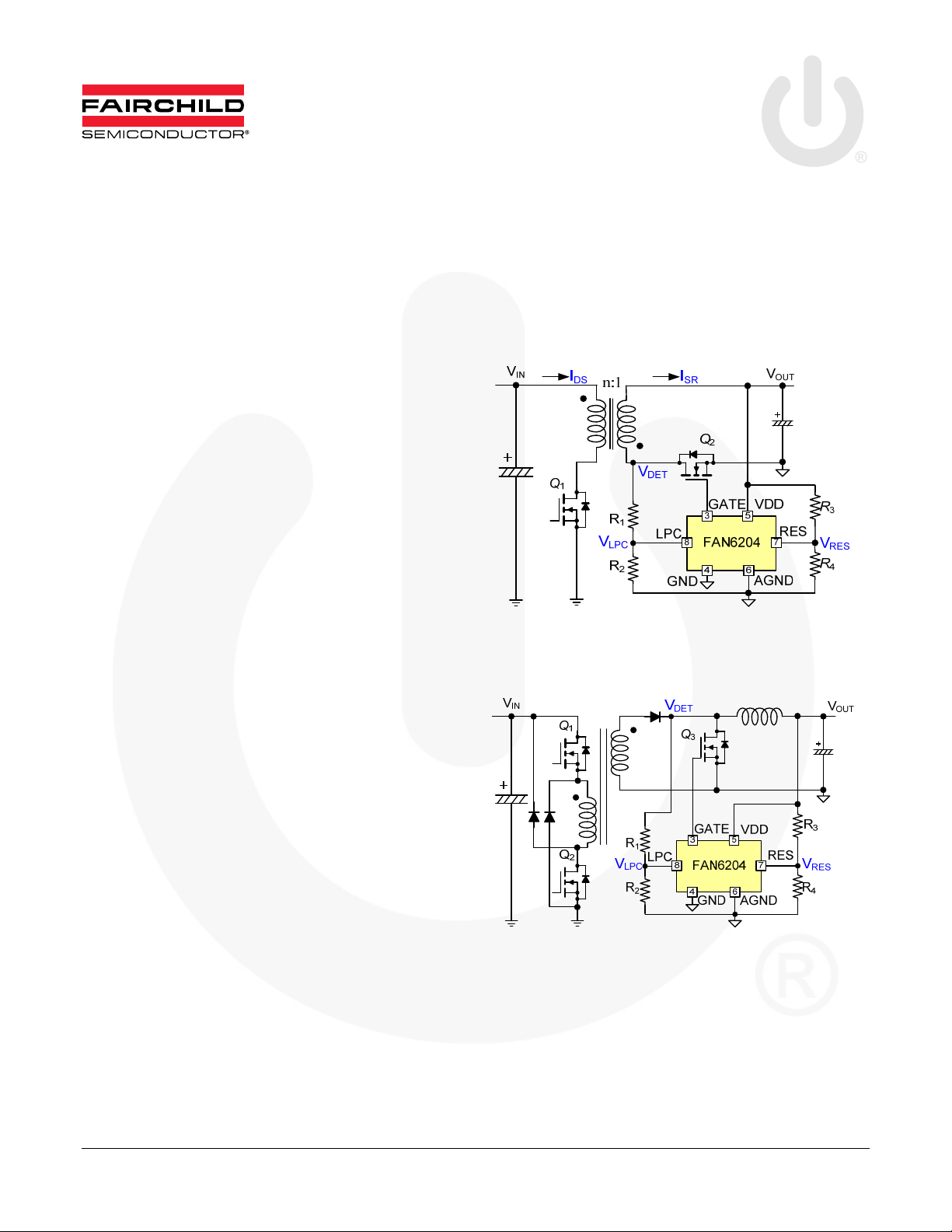
and dual-switch forward free-wheeling rectification (Figure
1 and Figure 2).
FAN6204 utilizes a proprietary innovative linear-predict
timing control to determine the turn-on and turn-off timing
of SR MOSFET. This control technique detects the voltage
of the transformer winding and output voltage instead of
MOSFET current, so noise immunity can be accomplished.
Furthermore, this technique doesn’t need a communication
signal from the primary side, so this feature reduces external
components and simplifies PCB layout.
Figure 1. Typical Application Circuit for
Flyback Converter
In abnormal test conditions, since Linear-Predict Timing
control (LPT) and causal function may not guarantee safe
operation, some protection functions should be applied.
Fault Causal Timing protection, Gate Expand Limit
protection, and RES dropping protection are used for loadchange test condition. LPC and RES pins’ open/short
protection is to prevent fault operation of SR controller if
LPC/RES resistors are damaged. In addition, internal OverTemperature Protection (OTP) and V
Protection ( VDD OVP) are also included to avoid a timing
sequence where FAN6204 is uncontrollable under hightemperature or output over-voltage condition.
To improve no-load or light-load efficiency, a Green Mode
function is utilized. In Green Mode, the SR controller stops
all SR switching to reduce the operating current, keeping
power consumption at low levels in light-load condition.
© 2011 Fairchild Semiconductor Corporation www.fairchildsemi.com
Rev. 1.0.1 • 11/10/11
Over-Voltage
DD
Figure 2. Typical Application Circuit for Dual-Switch
Forward Free-Wheeling Rectification

AN-6204 APPLICATION NOTE
External Components Design
(a) Flyback Rectification Application
As shown in Figure 1, the resistors on the LPC and RES
pins need to be designed appropriately for LPT control.
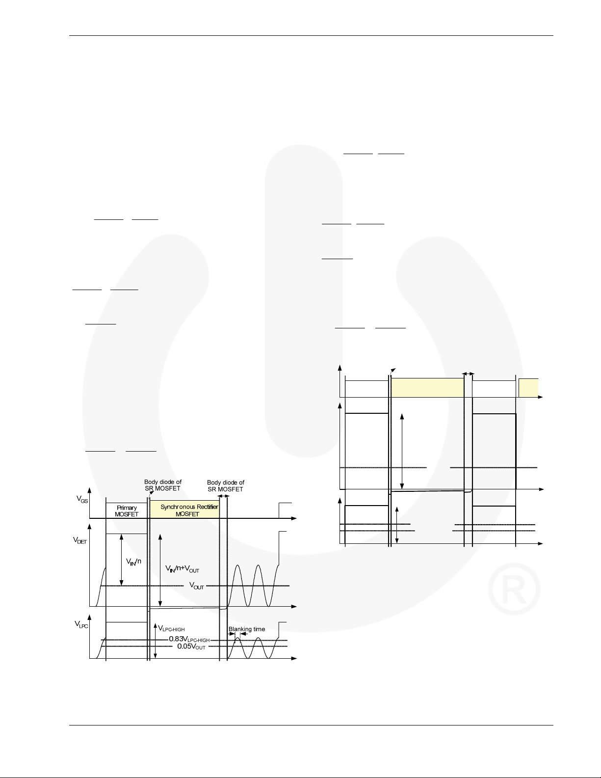
Referring to Figure 3, when LPC voltage is higher than
over a blanking time (t
V
LPC-EN
output. After LPC voltage drops below V
(0.05V
V
LPC-EN
), SR MOSFET starts to output. Therefore,
OUT
must be higher than V
MOSFET cannot be turned on. Consequently, the voltage
divider of LPC, R
R
2
0.83 ( ) 0.05 0.3
RR n
12
and R2, should be considered as:
1
V
.
IN MIN
VV
OUT OUT
On the other hand, the linear operating range of LPC and
RES (1~4V) should also be considered as:
V
R
2
RR n
12
14
RR
34
.
IN MAX
()4
R
4
V
OUT
V
OUT
), SR gate is ready to
LPC-EN
LPC-TH-HIGH
or the SR
LPC-TH-HIGH
(1)
(2)
(3)
(b) Dual-Switch Forward Free-Wheeling
Rectification Application:
Figure 2 shows a typical application circuit for applying
FAN6204 on forward free-wheeling diode rectification.
V
LPC-EN
must be higher than V
LPC-TH-HIGH
so the voltage
divider of LPC, R1 and R2, should be considered as:
V
0.83 0.05 0.3
R
2
RR n
12
.
IN MIN
V
OUT
The linear operating range of LPC and RES (1~4V)
should also be considered as:
V
R
2
RR n
12
R
4
.
IN MAX
V
OUT
RR
43
4
4
Considering the tolerance of voltage divider resistors and
internal circuit, the scale-down ratio (K) is set to 5~5.5.
RR
24
K
RR RR
12 34
(5)
(6)
(7)
(8)
Since the voltage scale-down ratio between RES and LPC
(K) is 5, the discharge time of C
(t
T
inductor current discharge time (t
) is same as the
CT.DIS
). However,
L.DIS
considering the tolerance of voltage divider resistors and
internal circuit, the scale-down ratio (K) should be larger
than 5 to guarantee that t
is shorter than t
CT.DIS
L.DIS
. It is
typical to set K to 5~5.5.
RR
K
24
RR RR
12 34
(4)
Body diode of
SR MOSFET
V
GS
Primary
MOSFET
V
DET
V
LPC
Synchronous Rectifier
MOSFET
VIN/n
V
LPC-HIGH
0.83V
0.05V
V
OUT
LPC-HIGH
OUT
Body diode of
SR MOSFET
Figure 4. Typical Waveforms of Forward
Free-Wheeling Rectification with FAN6204
Primary
MOSFET
Figure 3. Typical Waveforms of QR Flyback Converter
with FAN6204
© 2011 Fairchild Semiconductor Corporation www.fairchildsemi.com
Rev. 1.0.1 • 11/10/11 2

AN-6204 APPLICATION NOTE
(c) Consideration of External Component Value
LPC Part: To prevent LPC pin damage by negative
voltage while V
drops below V
LPC
FAN6204 sources a current, I
to clamp V
at a positive voltage level. To operate
LPC
LPC-SOURCE
LPC-SOURCE
, from the LPC pin
(0.2V),
regularly, the clamped voltage level must be lower than
V
LPC-TH-HIGH
clamped voltage cannot be under V
, so R2 should not be too large. While the low
LPC-TH-HIGH
, R2 should
be decreased to guarantee proper operation of SR
controller. Once R2 is decided, R1 can also be determined
due to calculated LPC ratio. The recommended value of
R2 is under 15kΩ. In addition, if the noise interference is
serious, a ceramic capacitor (around 10pF to 22pF)
parallel on LPC pin is recommended.
RES Part: For power saving, the values of R
and R4 are
3
designed as large as possible (theoretically). Actually,
since high-impedance components can cause noise
interference, the values of RES resistors should not be
designed too large. For the reason, the recommended
value is 10kΩ to several hundred kΩ.
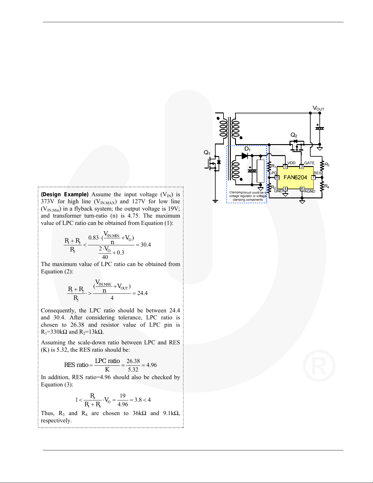
(Design Example) Assume the input voltage (V
373V for high line (V
) in a flyback system; the output voltage is 19V;
(V
IN.Min
) and 127V for low line
IN.MAX
IN
) is
and transformer turn-ratio (n) is 4.75. The maximum
value of LPC ratio can be obtained from Equation (1):
VDD Section
Output voltage (V
while V
is regulated between 5V and 24V. If VO is not
O
) can be applied as VDD of FAN6204,
O
regulated in that range, an additional winding of
transformer can be utilized to provide energy to V
DD
. The
simplified circuit is shown as Figure 5. To prevent the
variation of the V
supply voltage, use a voltage
DD
regulator or voltage clamping components, such as a
Zener diode, to clamp V
voltage in a proper range.
DD
Clamping
Circuit
Figure 5. Simplified Circuit of Additional Winding
Supply
for V
DD
V
.
RR
12
R
2
0.83 ( )
IN MIN
2
V
40
V
O
n
O
0.3
30.4
The maximum value of LPC ratio can be obtained from
Equation (2):
V
.
IN MAX
V
RR
12
R
()
2
OUT
n
4
24.4
Consequently, the LPC ratio should be between 24.4
and 30.4. After considering tolerance, LPC ratio is
chosen to 26.38 and resistor value of LPC pin is
=330kΩ and R2=13kΩ.
R
1
Assuming the scale-down ratio between LPC and RES
(K) is 5.32, the RES ratio should be:
LPC ratio
RES ratio
4.96
26.38
K
5.32
In addition, RES ratio=4.96 should also be checked by
Equation (3):
Thus, R
R
4
1 3.8 4
RR
34
and R4 are chosen to 36kΩ and 9.1kΩ,
3
19
V
O
4.96
respectively.
© 2011 Fairchild Semiconductor Corporation www.fairchildsemi.com
Rev. 1.0.1 • 11/10/11 3
 Loading...