FAN5904 — Multi-Mode Buck Converter for GSM/EDGE, 3G/3.5G and 4G PAs
December 2011
FAN5904
Multi-Mode Buck Converter for GSM/EDGE, 3G/3.5G and 4G PAs
Features
2.7V to 5.5V Input Voltage Range
V
Range from 0.40V to 3.50V (or VIN)
OUT
Single 470nH Small Form Factor Inductor
35mΩ Integrated Bypass FET
100% Duty Cycle for Low Dropout Operation
Input Under-Voltage Lockout / Thermal Shutdown
1.71mm x 1.71mm, 16-Bump, 0.40mm Pitch WLCSP
High Power PWM Mode
o Up to 95% Efficient Synchronous Operation in
High P
o Output current up to 2.3A
o 10µs Output Voltage Step Response for Early
GSM Tx Power-Loop Settling
o 3MHz PWM Mode
Conditions
OUT
Low Power Auto Mode
o Up to 95% Efficient Synchronous Operation at
Higher P
o Output Current up to 1.2A
o 10µs Output Voltage Step Response for Early Tx
Power-Loop Settling
o 6MHz PWM Operation at High Power and PFM
Operation at Low Power
Conditions
OUT
Bypass Mode
o Up to 3A Load Current
Applications
Dynamic Supply Bias for Polar or Linear GSM/EDGE
PAs and 3G/3.5G and 4G PAs
Dynamic Supply Bias for GSM/EDGE Quad Band
Amplifiers for Mobile Handsets and Data Cards
Description
The FAN5904 is a high-efficiency, low-noise, synchronous,
step-down, DC-DC converter optimized for powering Radio
Frequency (RF) Power Amplifiers (PAs) in handsets and
other mobile applications. In High-Power Mode, GSM Tx
power is enabled. In Low-Power Mode, up to 3.0W is
supported, enabling up to 29dBm output power for 3G/3.5G
and 4G platforms.
The output voltage may be dynamically adjusted from 0.40V
to 3.50V, proportional to an analog input voltage VCON
ranging from 0.16V to 1.40V, optimizing power-added
efficiency. Fast transition times of less than 10µs are
achieved, allowing excellent inter-slot settling.
An integrated bypass FET is automatically enabled when
the battery voltage and voltage drop across the DC-DC
PMOS device are within a set voltage range of the desired
output voltage (V
bypass feature enables the FAN5904 to support heavy load
currents under the most stringent VSWR conditions while
maintaining high efficiency and superior spectral
performance. The bypass FET may also be enabled by
providing a VCON voltage nominally greater than or equal
to 1.5V or by driving BPEN high.
The FAN5904 operates in PWM Mode with a 6MHz
switching frequency in Low-Power Mode and at 3MHz in
High-Power Mode, which limits high-frequency spur levels.
It uses a single, small form factor inductor of 470nH. In
addition, PFM operation is allowed in Low-Power Mode to
improve efficiency at low load currents.
The FAN5904UC00X option allows PFM Mode only when
is less than 1V, while the FAN5904UC01X permits
V
OUT
PFM Mode at higher voltages for applications that can
tolerate larger output ripple and that demand optimal low-tomoderate load current efficiency.
OUT
= V
BAT
- V
PMOS
- V
). This dynamic
BP_TH
Ordering Information
Part Number LPM Mode PFM Output Voltage
FAN5904UC00X V
FAN5904UC01X All V
© 2011 Fairchild Semiconductor Corporation www.fairchildsemi.com
FAN5904 • Rev. 3.0.5
OUT
< 1V
OUT
0.4V to PVIN -40°C to +85°C
Temperature
Range
Package Packing
1.71mm x 1.71mm, 16-Bump
0.4mm Pitch, Wafer-Level
Chip-Scale Package (WLCSP)
Tape and Reel

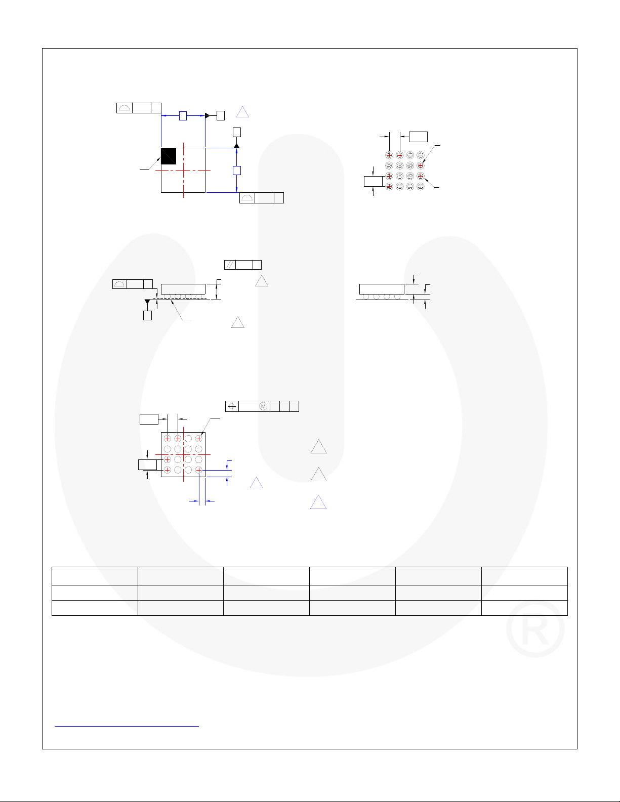
Physical Dimensions
FAN5904 — Multi-Mode Buck Converter for GSM/EDGE, 3G/3.5G and 4G PAs
2X
BALL A1
INDEX AREA
0.03 C
0.05 C
C
0.40
0.40
BOTTOM VIEW
E
TOP VIEW
SEATING
PLANE
2
3
1
4
A
B
D
0.625
0.547
Ø0.260±0.02
16X
D
C
B
(Y) ±0.018
A
(X) ±0.018
0.06 C
D
F
0.03 C
2X
E
SIDE VIEWS
0.005 CAB
F
0.40
A1
0.40
(Ø0.20)
Cu Pad
(Ø0.30) Solder
Mask Opening
RECOMMENDED LAND PATTERN
(NSMD PAD TYPE)
0.378±0.018
0.208±0.021
NOTES:
A. NO JEDEC REGISTRATION APPLIES.
B. DIMENSIONS ARE IN MILLIMETERS.
C. DIMENSIONS AND TOLERANCE
PER ASME Y14.5M, 1994.
D. DATUM C IS DEFINED BY THE SPHERICAL
CROWNS OF THE BALLS.
E. PACKAGE NOMINAL HEIGHT IS 586 MICRONS
±39 MICRONS (547-625 MICRONS).
F. FOR DIMENSIONS D, E, X, AND Y SEE
PRODUCT DATASHEET.
G. DRAWING FILNAME: MKT-UC016AArev2.
Product D E X Y Unit
FAN5904UC00X 1.710 ±0.030 1.710 ±0.030 0.255 0.255 mm
FAN5904UC01X 1.710 ±0.030 1.710 ±0.030 0.255 0.255 mm
Figure 60. 1.71x1.71mm Square, 16 Bumps, 0.4mm Pitch, WLCSP
Package drawings are provided as a service to customers considering Fairchild components. Drawings may change in any manner without
notice. Please note the revision and/or date on the drawing and contact a Fairchild Semiconductor representative to verify or obtain the most
recent revision. Package specifications do not expand the terms of Fairchild’s worldwide terms and conditions, specifically the warranty
therein, which covers Fairchild products.
Always visit Fairchild Semiconductor’s online packaging area for the most recent package drawings:
http://www.fairchildsemi.com/packaging/
© 2011 Fairchild Semiconductor Corporation www.fairchildsemi.com
FAN5904 • Rev. 3.0.5 22
 Loading...