Fairchild FAN5903 service manual

December 2011
FAN5903
Buck Converter with Bypass Mode for 3G/3.5G/4G PAs
FAN5903 — Buck Converter with Bypass Mode for 3G/3.5G/4G PAs
Features
2.7V to 5.5V Input Voltage Range
V
Range from 0.4V to 3.50V (or VIN)
OUT
Small Form Factor Inductor
o 2012 470nH or 540nH for Minimal PCB Area
o 2020 1.0µH for Higher Efficiency
Bypass Dropout at 500mA, 60mV Typical
100% Duty Cycle for Low Dropout Operation
Input Under-Voltage Lockout / Thermal Shutdown
1.34mm x 1.29mm, 9-Bump, 0.4mm-Pitch WLCSP
3MHz / 6MHz Selectable Switching Frequency to
Facilitate System Optimization
High-Efficiency PFM Operation at Low Power
Sleep Mode for Very Low I
Operation
Q
Up to 96% Efficient Synchronous Operation at
High-Power Conditions
10µs Output Voltage Step Response for Early
Power Loop Settling
Applications
Dynamic Supply Bias for 3G/3.5G and 4G PAs
Power Supply for WCDMA/LTE PAs
Resources
For more information or a full copy of this datasheet,
please contact a Fairchild representative.
Description
FAN5903 is a high-efficiency, low-noise, synchronous,
step-down, DC-DC converter designed for powering
3G/3.5G/4G RF Power Amplifiers (PAs) in handsets and
other mobile applications.
The output voltage may be dynamically varied from
0.40V to 3.50V, proportional to an analog input V
ranging from 0.16V to 1.40V provided by an external
DAC. This allows the PA to be supplied with the voltage
that enables maximum power-added efficiency.
An integrated bypass FET automatically switches on
when battery voltage drops close to the desired output
voltage (V
to Synchronous Mode when the voltage dropout
exceeds 375mV. The integrated bypass FET is also
enabled when V
The FAN5903 offers fast transition times, enabling
changes to the output voltage in less than 10µs for
power transitions. Moreover, a Current-Mode control
loop with fast transient response ensures excellent line
and load regulation.
Light-load efficiency is optimized by operating in PFM
Mode for load currents typically less than 100mA.
The switching frequency may be set to 3MHz or 6MHz,
enabling further optimization of system performance.
The FAN5903 typically uses a single, small-form-factor
inductor of 540nH. Efficiency may be further optimized
using a 1.0µH inductor when running at 3MHz.
When output regulation is not required, the FAN5903
may be placed in Sleep Mode by setting V
to 100mV. This ensures a very low I
enabling a fast return to output regulation. The
FAN5903 enables significant current reduction and
increased talk time and is available in a 1.34mm x
1.29mm, 9-bump, 0.40mm-pitch, WLCSP package.
OUT=VBAT
-200mV). The DC-DC switches back
is nominally greater than to 1.5V.
CON
nominally
CON
(<70µA) while
Q
CON
,
Ordering Information
Part Number
FAN5903UCX -40 to +85°C
© 2008 Fairchild Semiconductor Corporation www.fairchildsemi.com
FAN5903 • Rev. 1.0.7
Operating
Temperature Range
1.34mm x 1.29mm, 9-bump, 0.4mm Pitch,
Wafer-Level Chip-Scale Package (WLCSP)
Package Packing Method
Tape and Reel

Physical Dimensions
FAN5903 — Buck Converter with Bypass Mode for 3G/3.5G/4G PAs
2X
PIN A1
INDEX AREA
0.05
0.03
C
TOP VIEW
C
C
E
SEATING PLANE
A
B
D
0.539
0.461
D
F
0.03
2X
0.06
C
E
SIDE VIEWS
0.40
A1
0.40
C
Ø0.20
Cu Pad
Ø0.30
Solder Mask
LAND PATTERN RECOMMENDATION
(NSMD PAD TYPE)
0.292±0.018
0.208±0.021
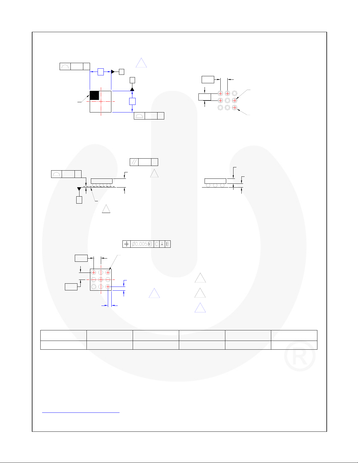
NOTES:
A. NO JEDEC REGISTRATION APPLIES.
0.40
0.40
123
BOTTOM VIEW
Ø0.260±0.020
9X
C
B
(Y)±0.018
A
(X)±0.018
F
B. DIMENSIONS ARE IN MILLIMETERS.
C. DIMENSIONS AND TOLERANCE
PER ASMEY14.5M, 1994.
D. DATUM C IS DEFINED BY THE SPHERICAL
CROWNS OF THE BALLS.
E. PACKAGE NOMINAL HEIGHT IS 500 MICRONS
±39 MICRONS (461-539 MICRONS).
F. FOR DIMENSIONS D, E, X, AND Y SEE
PRODUCT DATASHEET.
G. DRAWING FILNAME: MKT-UC009AErev1
Product D E X Y Unit
FAN5903UCX 1.292 ± 0.030 1.342 ± 0.030 0.271 0.246 mm
Figure 42. 1.34 x 1.29mm, 9-Bump, 0.4mm-Pitch WLCSP
Package drawings are provided as a service to customers considering Fairchild components. Drawings may change in any manner
without notice. Please note the revision and/or date on the drawing and contact a Fairchild Semiconductor representative to verify or
obtain the most recent revi sion. Package specifications do not expand the terms of Fairchild’s worldwide terms and conditions, specifically the
warranty therein, which covers Fairchild products.
Always visit Fairchild Semiconductor’s online packaging area for the most recent package drawings:
http://www.fairchildsemi.com/packaging/.
© 2008 Fairchild Semiconductor Corporation www.fairchildsemi.com
FAN5903 • Rev. 1.0.7 18
 Loading...