Fairchild FAN5665 service manual
February 2008
FAN5665
High-Efficiency, Adaptive Charge Pump 5V Boost
FAN5665 — High-Efficiency, Adaptive Charge Pump 5V Boost
Features
5V Fixed Output Voltage
30mA Maximum Output Current
Built-in Charge Pump with Three Modes of
Operation: 1×, 1.5×, and 2×
Minimum External Components
Flying Capacitors Only 0.22µF
Low-noise, Constant-frequency Operation (1.2MHz)
at Heavy Loads
High-efficiency, Low-frequency Operation at Light
Loads
Low Quiescent Current
Up to 92% Efficiency
2.9V to 5.5V Input Voltage Range
Soft-start for Limiting Inrush Current
Input Under-Voltage Lockout Protection (UVLO)
Short-Circuit Protection (SCP)
Thermal Shutdown Protection (TSD)
8-bump 1.21 x 1.21mm, 0.4mm Pitch WLCSP
Applications
USB I/O Supply Regulators
Cell Phones, Smart-Phones
Pocket PCs
PDA, DSC, PMP, and MP3 Players
Description
The FAN5665 is a 5V switched capacitor step-up
DC/DC converter with an input voltage range from 2.9V
to 5.5V. Switch reconfiguration and fractional switching
techniques are utilized to achieve high efficiency over
the entire input voltage range.
The FAN5665 includes built-in under-voltage lockout,
short circuit, and thermal protection circuitry.
The FAN5665 is available in an 8-bump 0.4mm pitch
WLCSP package.
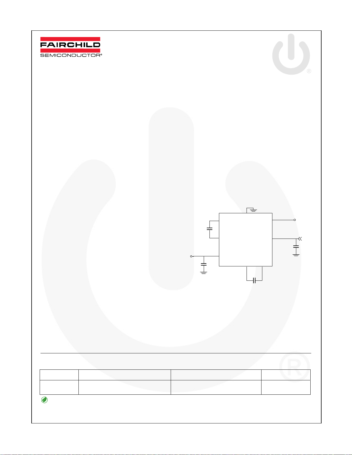
+5V
C
OUT
2.2µF
C1-
C1
0.22µF
C1+
VOUT
Figure 1. Typical Application
GND
C2+
EN
VIN
C2-
C2
0.22µF
+2.9 to 5. 5V
C
IN
2.2µF
Ordering Information
Part Number Operating Temperature Range Package Packing Method
FAN5665UCX
All packages are lead free per JEDEC: J-STD-020B standard.
© 2007 Fairchild Semiconductor Corporation www.fairchildsemi.com
FAN5665 • Rev. 1.0.1
-40°C to +85°C
8-Lead Wafer-Level Chip-Scale
Package (WLCSP), 1.21x1.21mm
Tape and Reel
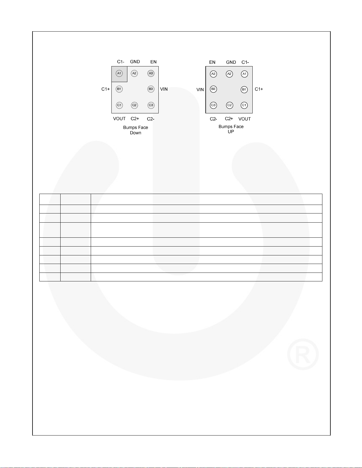
Pin Configuration
Pin Definitions
FAN5665 — High-Efficiency, Adaptive Charge Pump 5V Boost
Figure 2. Pin Configuration
Pin # Name Description
A1 C1- Bucket capacitor 1. Connect this pin to the negative terminal of the bucket (flying) capacitor.
A2 GND
A3 EN
B1 C1+ Bucket capacitor 1. Connect this pin to the positive terminal of the bucket (flying) capacitor.
B3 VIN Power input.
C1 VOUT Regulated 5V output.
C2 C2+ Bucket capacitor 2. Connect this pin to the positive terminal of the bucket (flying) capacitor.
C3 C2- Bucket capacitor 2. Connect this pin to the negative terminal of the bucket (flying) capacitor.
Ground.
Enable. Enables the IC when high. Disables the IC when low and enters shutdown mode.
No internal pull-up or pull-down; this pin should not be left floating.
© 2007 Fairchild Semiconductor Corporation www.fairchildsemi.com
FAN5665 • Rev. 1.0.1 2
FAN5665 — High-Efficiency, Adaptive Charge Pump 5V Boost
Absolute Maximum Ratings
Stresses exceeding the absolute maximum ratings may damage the device. The device may not function or be
operable above the recommended operating conditions and stressing the parts to these levels is not recommended.
In addition, extended exposure to stresses above the recommended operating conditions may affect device
reliability. The absolute maximum ratings are stress ratings only.
Symbol Parameter Min. Max. Unit
VIN
TJ Junction Temperature –40 +150 °C
T
STG
TL Lead Soldering Temperature, 10 Seconds +260 °C
ESD
VIN Pin –0.3 +6.0 V
EN, VOUT, C1+, C1-, C2+, C2- Pins –0.3 +6.0 V
Storage Temperature –65 +150 °C
Human Body Model, JESD22-A114 3.5
Charged Device Model, JESD22-C101 2
kV
Recommended Operating Conditions
The Recommended Operating Conditions table defines the conditions for actual device operation. Recommended
operating conditions are specified to ensure optimal performance to the datasheet specifications. Fairchild does not
recommend exceeding them or designing to Absolute Maximum Ratings.
Symbol Parameter Min. Typ. Max. Unit
VIN Power Supply Range 2.9 5.5 V
I
Output Current 0 30 mA
OUT
TA Operating Ambient Temperature Range –40 +85 °C
TJ Operating Junction Temperature Range –40 +125 °C
CIN, C
Input, output capacitor 2.2 µF
OUT
C1, C2 Bucket capacitor 0.22 µF
Thermal Properties
Symbol Parameter Min. Typ. Max. Units
ΘJA Junction-to-Ambient Thermal Resistance 170
Note:
1. Junction-to-ambient thermal resistance is a function of application and board layout. This data is measured with
four-layer boards in accordance with JESD51- JEDEC standard. Special attention must be paid not to exceed
maximum junction temperature (T
) at a given ambient temperate (TA).
J
(1)
°C/W
© 2007 Fairchild Semiconductor Corporation www.fairchildsemi.com
FAN5665 • Rev. 1.0.1 3
Electrical Characteristics
Unless otherwise noted, V
test circuit is Figure 1. Typical values are at T
Symbol Parameter Conditions Min. Typ. Max. Units
Power Supplies
ISD Shutdown Current VIN = 3.6V 0.1 1.0 µA
IDD Quiescent Current
VIH Enable High-level Input Voltage 1.1
VIL Enable Low-level Input Voltage 0.4
IIH Enable Pin Input Current EN = 1.8V 0.01 1.00
V
Under-voltage Lockout High Threshold VIN Rising 2.60 2.80
HUVLO
V
Under-voltage Lockout Low Threshold VIN Falling 2.30 2.60 V
LUVLO
UVLO Hysteresis 250 mV
Regulation
V
Voltage Accuracy 4.85 5.00 5.15 V
OUT
V
OUT_RIPPLE
TSD Thermal Shutdown
Timing
Note:
2. Guaranteed by design.
Output Voltage Ripple
ISC Short-Circuit Current Limit V
f
Internal Oscillator Frequency
OSC
tss Soft-start EN = 0 to 1 570 950
= 2.9V to 5.5V, C1 = C2 = 0.22µF, CIN = 2.2µF, C
IN
= 25°C, VIN = 3.6V.
A
VIN = 3.6V, I
= 5.5V, I
V
IN
VIN = 3.6V, I
V
= 3.6V, I
IN
< 150mV 45 55 80 mA
OUT
= 0mA 190 300
OUT
= 0mA 108 200
OUT
= 2mA 25
OUT
= 30mA 15
OUT
Rising Temperature 150
Hysteresis 20
VIN = 3.6V, I
V
= 3.6V, I
IN
= 20mA 0.9 1.2 1.5 MHz
OUT
= 2mA 40 49 65 kHz
OUT
= 2.2µF, TA = -40°C to +85°C, and
OUT
(2)
µA
V
V
µA
V
mV
°C
µs
FAN5665 — High-Efficiency, Adaptive Charge Pump 5V Boost
pp
© 2007 Fairchild Semiconductor Corporation www.fairchildsemi.com
FAN5665 • Rev. 1.0.1 4
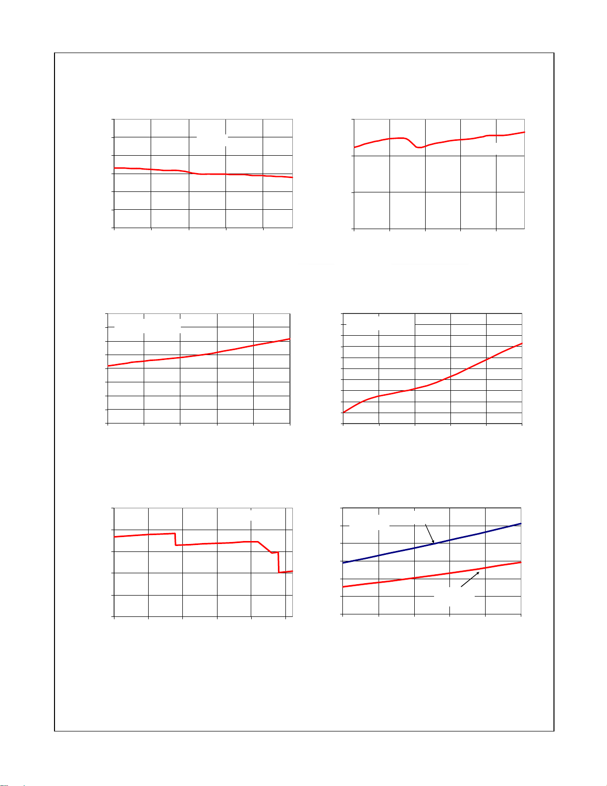
Typical Performance Characteristics
Unless otherwise noted, CIN = 2.2µF, C
= 2.2µF, C1 = C2 = 0.22µF, TA = 25°C.
OUT
50.5
FAN5665 — High-Efficiency, Adaptive Charge Pump 5V Boost
1.2163
50.0
49.5
49.0
48.5
48.0
Switc hi ng Fr equency ( kHz)
47.5
2.93.43.94.44.9
I
=2mA
OUT
Input Voltage (V)
Figure 3. Light-Load Switching Frequency
vs. Input Voltage
80
VIN=3.6V, I
70
60
50
40
30
20
10
Switching Frequecy (kHz)
0
-40 -15 10 35 60 85
=2mA
OUT
Temperature (°C)
Figure 5. Light-Load Switching Frequency
vs. Temperature
I
=20mA
1.2042
1.1921
Switching Fr eque ncy ( M Hz )
1.1800
2.9 3.4 3.9 4.4 4.9
Input Voltage (V)
OUT
Figure 4. Heavy-Load Switching Frequency
vs. Input Voltage
1.34
VIN=3.6V , I
1.32
1.30
1.28
1.26
1.24
1.22
1.20
1.18
Swit c hi ng Fr equec y ( M Hz)
1.16
1.14
-40 -15 10 35 60 85
=20mA
OUT
Temperature (°C)
Figure 6. Heavy-Load Switching Frequency
vs. Temperature
300
250
I
OUT
= 0mA
VIN=3.6V
A)
250
200
μ
I
OUT
=0mA
200
150
150
100
50
Quiescent Current (
0
2.9 3.4 3.9 4.4 4.9 5.4
Input Voltage (V)
100
50
Quiescent Curr e nt ( µA)
VIN=5.5V
0
-40 -15 10 35 60 85
Temperature (° C)
Figure 7. Quiescent Current vs. Input Voltage Figure 8. Quiescent Current vs. Temperature
© 2007 Fairchild Semiconductor Corporation www.fairchildsemi.com
FAN5665 • Rev. 1.0.1 5
 Loading...