Fairchild FAN5609 service manual

www.fairchildsemi.com
FAN5609
LED Driver with Adaptive Charge Pump DC/DC
Converter
Features
• Parallel LED Driver Supports All Forward Voltages
• Adaptive V
• Internally Matched LED Current Sources
• No External Components Needed to Set LED Current
• Built-in Charge Pump has Three Modes of Operation:
– Linear Regulation V
– 3/2 DC-DC Converter and Regulation 3.6V<V
– 2/1 DC-DC Converter and Regulation 2.7V<V
• Up to 86% Efficiency
• Low EMI, Low Ripple
• Up to 80mA Output Current (4 × 20mA)
• Built-in DAC for Digital or PWM Brightness Control
• Can be Duty Cycle Modulated between 0 to 18mA
• 2.7V to 5.5V Input Voltage Range
•I
< 2µA in Shutdown Mode
CC
• 1MHz Operating Frequency
• Shutdown Isolates Output from Input
• Soft-Start Limits Inrush Current
• Short Circuit Protection
• Minimal External Components Needed
• Available in a 14-lead TSSOP Package
• Available in a 16-lead MLP Package
Adjustment to the Highest Diode Voltage
OUT
> 4.2V
IN
<4.2V
IN
<3.6V
IN
Applications
• Cell Phones
• Handheld Computers
• PDA, DSC, MP3 Players
• Keyboard Backlight
• LED Displays
Description
The FAN5609 generates regulated output current from a
battery with input voltage varying between 2.7V to 5.5V.
Switch reconfiguration and fractional switching techniques
are utilized to achieve high efficiency over the entire input
voltage range. A proprietary internal circuitry continuously
monitors each LED current loop and automatically adjusts
the generated output DC voltage to the lowest minimum
value required by the LED having the highest forward
voltage. This adaptive nature of the FAN5609 eliminates the
need for LED pre-selection (matching) and ensures operation at high efficiency. When the input voltage is sufficiently
high to sustain the programmed current level in the LEDs,
the FAN5609 re-configures itself to operate as a linear
regulator, and the DC-DC converter is turned off. An internal
two-bit digital to analog converter provides programmability
of the output currents. Only two 0.1µF bucket capacitors and
two 4.7µF input/output capacitors are needed for proper
operation.
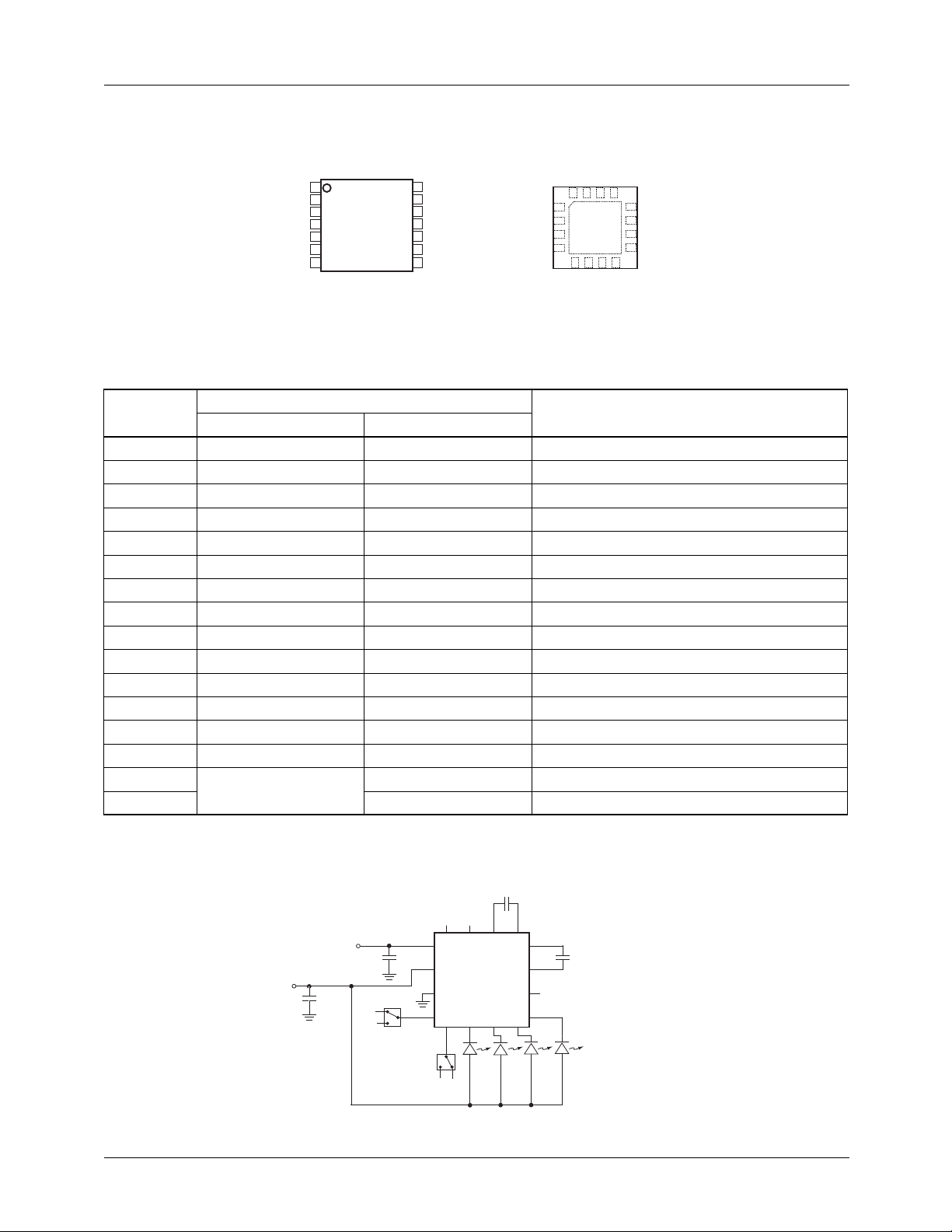
Typical Application
V
IN
Soft-start circuitry prevents excessive current draw during
power on. The device has built-in short circuit protection.
V
OUT
C
OUT
V
OUT
V
C
IN
IN
IN A
D
A
C
IN B
FAN5609
GND
LED-LED-LED-LED-
CAP-
CAP+
CAP+
CAP-
CAP2
CAP1
REV. 1.0.2 5/30/03

FAN5609 PRODUCT SPECIFICATION
Pin Assignments
Top-View
CAP2+
CAP2-
NC
V
GND
V
OUT
IN
B
NC
1
2
3
4
5
A
FAN5609
6
LED-
7
13141516
LED-
8
LED-
12
11
10
9
CAP1+
CAP1-
NC
LED-
V
IN
V
OUT
GND
B
FAN5609
A
LED-
LED-
FAN5609
14-Lead TSSOP
CAP2CAP2+
CAP1+
CAP1NC
LED-
LED-
4x4mm 16-Lead MLP
Pin Descriptions
FAN5609
Pin No.
1V
2V
IN
OUT
V
V
OUT
IN
Input
Output to LEDs Anode
3 GND GND Ground
4 B B DAC B
5 A A DAC A
6 LED - LED - 4th LED Cathode
7 LED - LED - 3rd LED Cathode
8 LED - LED - 2nd LED Cathode
9 LED - LED - 1st LED Cathode
10 NC NC No Connection
11 CAP1- CAP1- Bucket capacitor negative terminal
12 CAP1+ CAP1+ Bucket capacitor positive connection
13 CAP2+ CAP2+ Bucket capacitor positive terminal
14 CAP2- CAP2- Bucket capacitor negative connection
15 NC No Connection
16 NC No Connection
Pin Function Description14L-TSSOP 4mmX4mm 16L-MLP
Test Circuit
2
CAP2
13
0.1µF
12
8
CAP1
0.1µF
NC
9
4 White LEDs
Fairchild QTLP670C-IW
Super Bright LED
NCNC
= 2.7V to 5.5V
V
IN
C
V
OUT
4.7µF
C
OUT
IN
V
L
V
H
All capacitors are Ceramic chip capacitor
4.7µF
V
16
1
4
5
H
FAN5609
V
L
REV. 1.0.2 5/30/03

1
2 µ
PRODUCT SPECIFICATION FAN5609
Absolute Maximum Ratings
Parameter Min Max Unit
V
, V
IN
CAP+, CAP-, to GND -0.3 V
V
OUT
, A, B Voltage to GND -0.3 6.0 V
OUT
+ 0.3 V
IN
Short Circuit Duration INDEFINITE
Lead Soldering Temperature (10 seconds) 300 °C
Operating Junction Temperature Range 150 °C
Storage Temperature -55 150 °C
Electrostatic Discharge Protection Level (Note 1) HBM 4 kV
CDM 2
Recommended Operating Conditions
Parameter Min Typ Max Unit
Input Voltage Range, V
Operating Ambient Temperature Range -40 25 85 °C
2.7 5.5 V
IN
DC Electrical Characteristics
Unless otherwise noted, V
over the ambient operating temperature range.
Parameter Conditions Min. Typ. Max. Units
Quiescent Current V
Output Current Accuracy
I
= 20mA
NOM
LED to LED Current Matching V
Efficiency V
Input A, B Threshold Low
V
at Configuration
IN
Change
Oscillator Frequency
Supply Current, "OFF Mode"
Note:
1. Using Mil Std. 883E, method 3015.7(Human Body Model) and EIA/JESD22C101-A (Charge Device Model)
=3V to 5.5V, T
IN
A = B = High
From 1:1 to 3:2 4.2 V
From 3:2 to 2:1 3.6
= 25°C. Refer to “Test Circuit”. Boldface values indicate specifications
A
OUT
= 5.5V,
1.5 4 mA
No Load
A = High
17 20 23 mA
B = High
= 5.5V
IN
= 4.5V 85 to75 %
IN
V
= 3V 65 to 55
IN
High
-5 +5
0 0.3 × V
0.6 × V
IN
0.80
V
1.2
IN
IN
%
V
MHz
A
REV. 1.0.2 5/30/03
3

FAN5609 PRODUCT SPECIFICATION
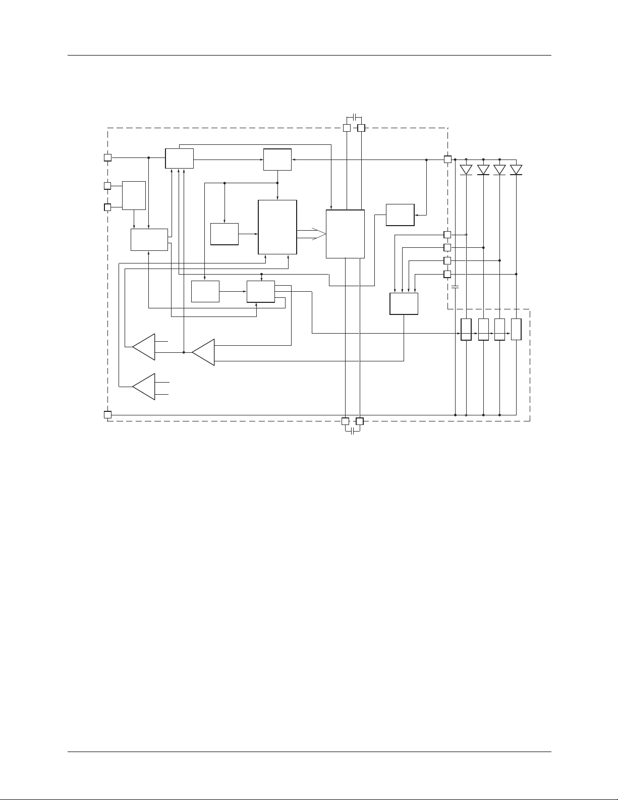
Block Diagram
1µF
V
OUT
And
Linear
Regulator
Oscillator
V
IN
A
DAC
B
On Off
Current Range
Voltage
Selector
D
R
I
V
E
R
S
Power
P
U
M
P
Good
Bandgap
Reference
Range Selection
Low Battery Ref.
Ref1
Mode Change
GND
VIN
Ref4 (BG)
Regulator
Reference
Ref3
Circuit Description
The FAN5609’s switched capacitor DC/DC converter automatically configures its internal switches to achieve high efficiency and to provide tightly regulated output currents for
the LEDs. An analog detector determines which diode
requires the highest voltage in order to sustain the pre-set
current levels, and adjusts the pump regulator accordingly.
Every diode has its own linear current regulator. In addition,
a voltage regulator controls the output voltage when the battery voltage is within a range where linear regulation can
provide maximum possible efficiency. If the battery voltage
is too low to sustain the diode current in the linear mode,
a fractional 3:2 charge pump is enabled. When the battery
voltage drops further and this mode is no longer sufficient to
sustain proper operation, the pump is automatically reconfigured to operate in 2:1 mode. As the battery discharges and
5µF
I. LIM.
I. LIM.
I. LIM.
I. LIM.
1µF
Ref2
Analog
Detector
the voltage decays, the FAN5609 switches between modes to
maintain a constant current through LED throughout the battery life. The transition has hysteresis to prevent toggling.
Supply Voltage
The internal supply voltage for the device is automatically
selected from V
Soft Start
The soft-start circuit limits inrush current when the device is
initially powered up and enabled. The reference voltage controls the rate of the output voltage ramp-up to its final value.
Typical start-up time is 1ms. The rate of the output voltage
ramp-up is controlled by an internally generated slow ramp,
and an internal variable resistor limits the input current.
IN
or V
pins, whichever is higher.
OUT
4
REV. 1.0.2 5/30/03
 Loading...