Fairchild FAN5608 service manual
www.fairchildsemi.com
FAN5608
Serial/Parallel LED Driver with Current-Regulated,
Step-Up DC/DC Converter
Features
• Two Independent Channels Drive up to Six LEDs per
Channel
• Adaptive Output Voltage Drive to Maximize Efficiency
• PWM/PFM Mode of Operation of the Boost Circuit
• Up to 85% Efficiency
• Up to 2 × 20mA Output
• Two Built-in DACs for Independent (Digital) Brightness
Control for Both Channels
• LED’s Current Can be Duty-Cycle-Modulated between
0 to 20mA
• Digital, Analog, and PWM Brightness Control
• 2.7V to 5.5V Input Voltage Range
• 0.5MHz Operating Frequency (8MHz internal clock)
• Soft Start
• Low Shutdown Current: I
CC
< 1
A
µ
• LED Short Circuit Protection
• Minimal External Components Needed
• Available in space saving 8-lead and 12-lead MLP
Packages.
Applications
• Cell Phones
• Handheld Computers
• PDAs, DSCs, MP3 Players
• Keyboard Backlights
• LED Displays
Description
The FAN5608 LED driver generates regulated output currents from a battery with input voltage varying between 2.7V
to 5V. An internal NMOS switch drives an external inductor,
and a Schottky diode delivers the inductor’s stored energy to
the load. Proprietary internal circuitry continuously monitors
the currrent on both strings and automatically adjusts the
generated output DC voltage to the lowest minimum value
required by the LEDs string with the highest summarized
forward voltage. This adaptive nature of the FAN5608
ensures operation at the highest possible efficiency. Soft start
circuitry prevents excessive current drawn from the supply
during power on. Any number of LEDs can be connected in
series as long as the summed forward voltages do not exceed
the specified operating output voltage range. Although it is
not required to have an equal number of LEDs connected in
series within each branch, the highest efficiency and best
current regulation is always achieved when an equal number
of LEDs are serially connected.
In the FAN5608 device, two internal two-bit D/A converters
provide independent programmability of each output channel
current. Analog programming of the output current is
also possible in the FAN5608. To do this, ground the "B"
pins and connect a resistor between the "A" pins and a
fixed supply voltage. The output current can then be
programmed to any desired value within its specified range.
The FAN5608DMPX/FAN5608MPX version uses a single
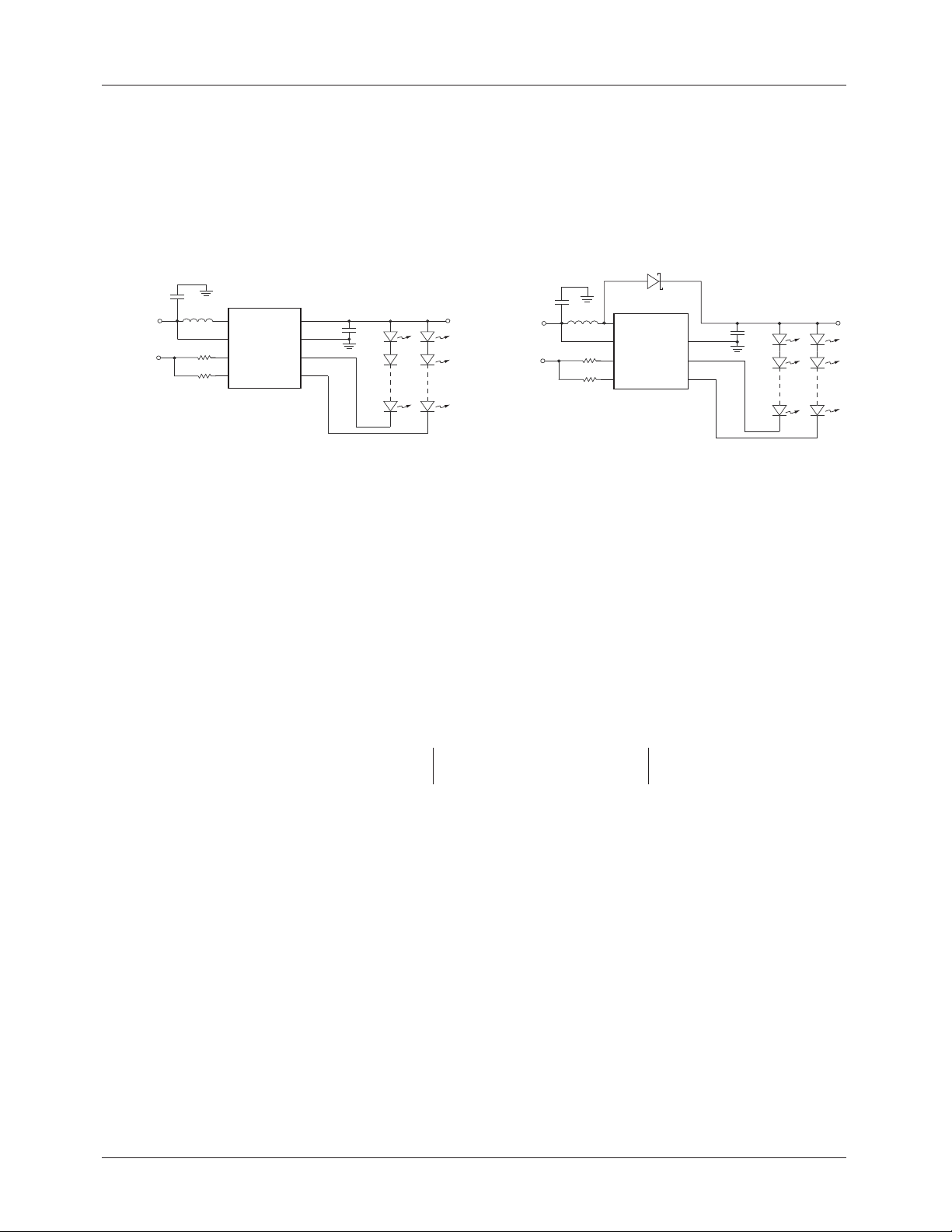
Typical Application
C
IN
2.7V to 5.5V
DAC Input For CH1
DAC Input For CH2
L = 4.7µH
IND
V
IN
A1
B1
A2
B2
4X4mm MLP-12 Package
with internal Schottky diode
Order Code: FAN5608DHMPX
FAN5608DHMPX
IND
V
GND
CH2
CH1
NC
OUT
Digital Brightness Control
C
IN
V
4.7µF
NN
OUT
2.7V to 5.5V
DAC Input For CH1
DAC Input For CH2
L = 4.7µH
IND
V
IN
A1
B1
A2
B2
4X4mm MLP-12 Package
with external Schottky diode
Order Code: FAN5608HMPX
IND
NC
GND
CH2
CH1
FAN5608HMPX
NC
4.7µF
REV. 1.0.4 1/7/05
V
OUT
PRODUCT SPECIFICATION FAN5608
external resistor to set the current, and to turn the device ON
and OFF. The FAN5608DMPX/FAN5608MPX is available
in an 8-lead MLP package with or without an internal Schot-
Typical Application
(Continued)
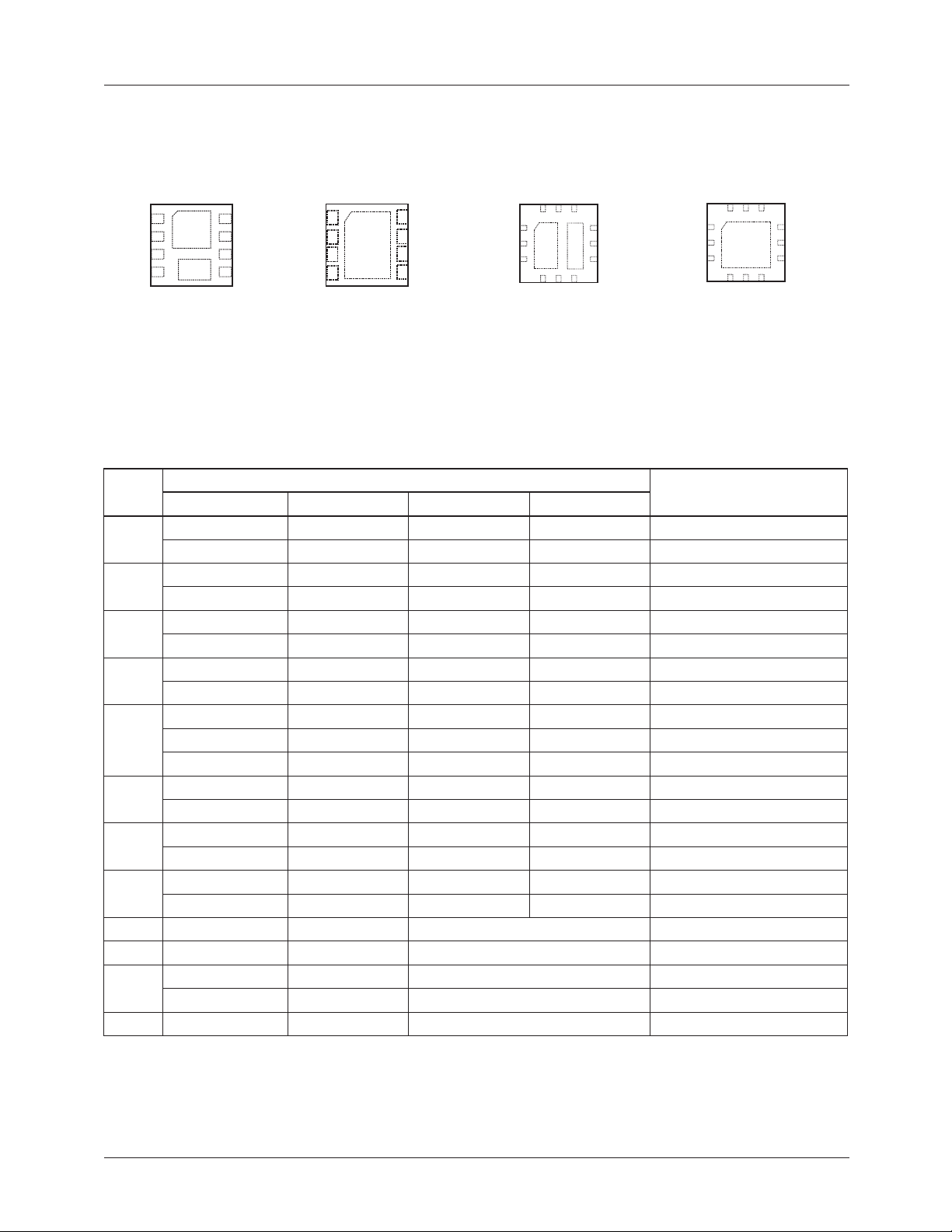
Analog Brightness Control
C
2.7V TO 5V
V
EXTERNAL
IN
L = 4.7µH
IND
IND
VIN
R
A1
R
A2
FAN5608DMPX
3X3mm MLP-8 Package
with internal Schottky diode
Order Code: FAN5608DMPX
V
OUT
GND
CH2
CH1
4.7µF
Definition of Terms
tky diode. The FAN5608DHMPX is available in a 12-lead
MLP package with an internal Schottky diode.
C
2.7V TO 5V
V
EXTERNAL
IN
IND
L = 4.7µH
IND
VIN
R
A1
R
A2
FAN5608MPX
3X3mm MLP-8 Package
with external Schottky diode
Order Code: FAN5608MPX
NC
GND
CH2
CH1
4.7µF
V
OUT
Output Current Accuracy: reflects the difference between the measured value of the output current (LED) and
programmed value of this current .
I
Output Current Accuracy (%)
------------------------------------------------------------------------------------------------------------=
OUT
measured I
I
OUT
programmed–()100×
OUT
programmed
Current Matching: refers to the absolute value of difference in current between the two LED branches.
Current Matching (%)
branch 1 I
LED
=
----------------------------------------------------------------------------------------------I
branch 1 I
LED
branch 2–()100×
LED
LED
branch 2+()2⁄
I
Efficiency: is expressed as a ratio between the electrical power into the LEDs and the total power consumed from the input
power supply.
Efficiency (%)
LED
--------------------------------------------------------------------------------------------------------------------------------------------------------------------------------------=
branch 1 I
branch 1× V
LED
V
INIIN
branch 1 I
LED
×
branch 1×+()100×
LED
V
Although this definition leads to a lower value than the boost converter efficiency, it more accurately reflects better system performance, from the user’s point-of-view.
2
REV. 1.0.4 1/7/05
FAN5608 PRODUCT SPECIFICATION
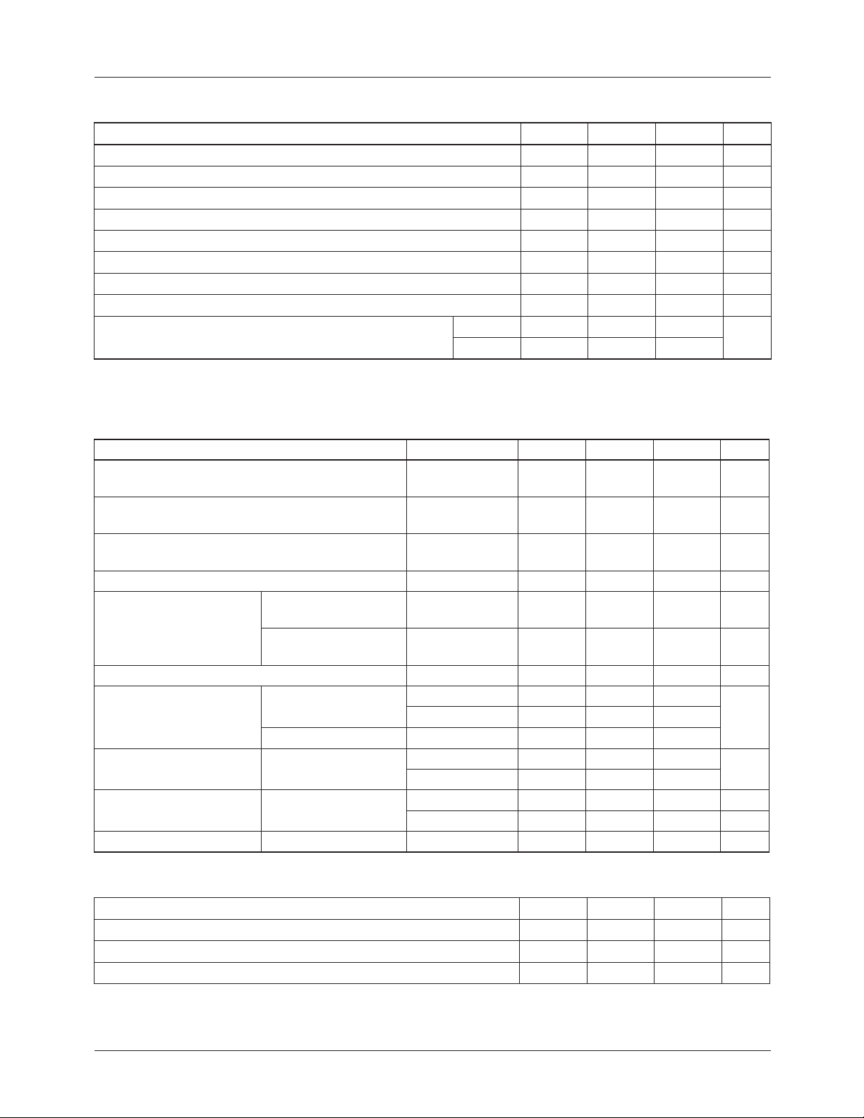
Pin Assignments
TOP-VIEW
NC
V
1
IN
2
A2
3
CH2
IND
45
A1
8
7
CH1
GND
6
V
NC IND
V
OUT
456
A1 A2
V
IN
1012 11
9
IND
8
CH2
7
B2
V
1
IN
2
A2
3
CH2
OUT
IND
4
8
A1
7
CH1
6
GND
5
NC
GND
CH1
1
2
3
B1
GND
CH1
B1
NC IND
1
2
3
456
V
A1 A2
IN
1012 11
9
IND
8
CH2
7
B2
3x3mm 8-Lead MLP
(Internal Schottky Diode)
FAN5608DMPX/FAN5608MPX
3x3mm 8-Lead MLP
(External Schottky Diode)
4x4mm 12-Lead MLP(QUAD)
(Internal Schottky Diode)
FAN5608DHMPX/FAN5608HMPX
4x4mm 12-Lead MLP(QUAD)
(External Schottky Diode)
Pin Descriptions
Pin No.
FAN5608DHMPX FAN5608HMPX FAN5608DMPX FAN5608MPX
1 GND GND GND GND Ground
2 CH1 CH1 1st LED Cathode
3 B1 B1 DAC B1
4 A1 A1 DAC A1
5V
IN
6 A2 A2 DAC A2
7 B2 B2 DAC B2
8 CH2 CH2 2nd LED Cathode
9 IND IND SD Anode
10 IND IND Inductor
11 V
OUT
12 NC NC No Connection
Pin Name
V
IN
V
IN
Pin Function Description
Input Voltage
A2 A2 DAC A2
CH2 CH2 2nd LED Cathode
IND IND Inductor
V
IN
V
OUT
Input Voltage
Output LEDs Anode
NC No Connection
GND GND Ground
CH1 CH1 1st LED Cathode
A1 A1 DAC A1
Output LEDs Anode
NC No Connection
REV. 1.0.4 1/7/05
3
3
PRODUCT SPECIFICATION FAN5608
Absolute Maximum Ratings
Parameter Min Typ Max Unit
V
, A, B Voltage to GND -0.3 6.5 V
IN
V
to GND -0.3 24 V
OUT
CH1, CH2 Voltage to GND 8 V
Any LED Short Circuit Duration (Anode to Cathode) Indefinite
Lead Soldering Temperature (10 seconds) 300 °C
Thermal Resistance θ
jc
8 °C/W
Operating Junction Temperature Range 150 °C
Storage Temperature Range -55 150 °C
Electrostatic Discharge (ESD) Protection (Note 1, 2) HBM 4 kV
CDM 1
DC Electrical Characteristics
= 2.7V to 5.5V, T
(V
IN
operating temperature.)
= 25°C, unless otherwise noted. Boldface values indicate specifications over the ambient
A
Parameter Conditions Min. Typ. Max. Units
Output Current Accuracy A = HIGH,
0.9 × I
NOM
I
= 20 1.1 × I
NOM
B = HIGH
Channel to Channel Current Matching A = HIGH,
B = HIGH
Efficiency (AVG) V
> 3.0V 80 %
IN
Switching Frequency 0.5 MHz
Multiplication Ratio FAN5608DMPX/
900 1000 1100
FAN5608MPX
FAN5608DHMPX/
850 1000 1150
FAN5608HMPX
Supply Current in OFF mode V
Input A1, A2 Threshold Digital
Mode
= V
= 0V 0.1
A
B
High V
-0.7 V
IN
Low 0 0.6
Analog Mode 1.2
Input B Threshold Digital Mode High 0.6 × V
IN
Low 0 0.3 × V
Input A1, A2 Current Digital Mode V
= V
A
IN
V
= 0 0.1 µA
A
50 60 µA
Input B1, B2 Current Digital Mode 0.1 µA
mA
NOM
%
A
µ
IN
V
IN
V
V
IN
Recommended Operating Conditions
Parameter Min Typ Max Unit
Input Voltage Range 2.7 5.5 V
Operating Ambient Temperature Range -40 25 85 °C
Output Voltage Range V
Notes:
1. Using Mil Std. 883E, method 3015.7(Human Body Model) and EIA/JESD22C101-A (Charge Device Model).
2. Avoid positive polarity ESD stress at the cathode of the internal Schottky diode.
IN
4
18 V
REV. 1.0.4 1/7/05
FAN5608 PRODUCT SPECIFICATION
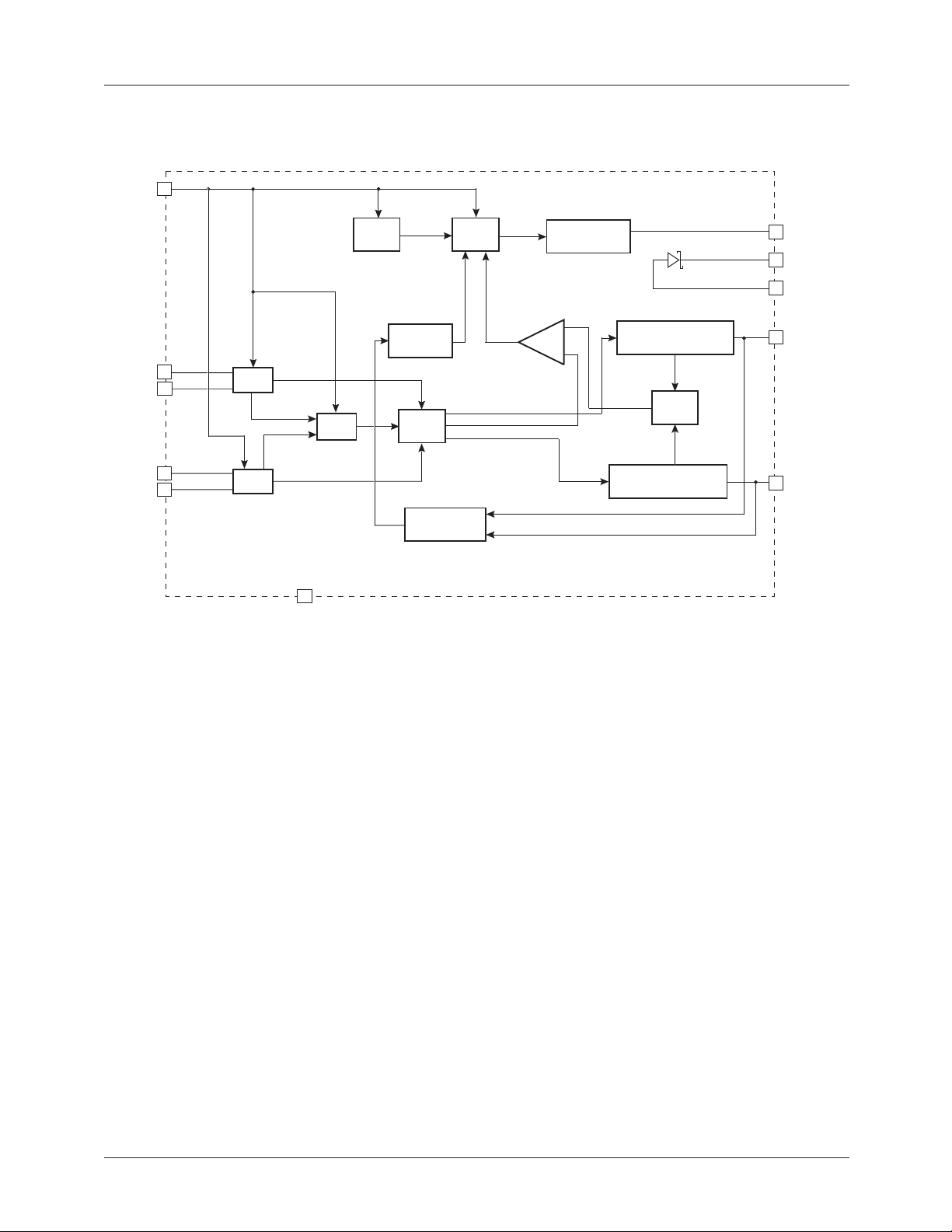
Block Diagram
V
IN
B1
A1
B2
A2
OSC
START-UP
DAC1
BG
DAC2
GND
Note: In the 8-pin version (analog version only), pins B1 and B2 are omitted.
REF
POWER GOOD
DBB
REF CH1
REF CH2
COIL DRIVER
LINEAR REGULATOR
LINEAR REGULATOR
W_OR
IND
V
OUT
IND
CH1
CH2
Circuit Description
When the input voltage is connected to V
turned on, the bandgap reference acquires its nominal voltage and the soft-start cycle begins. Once “power good” is
achieved (0.5mA in the diodes), the soft-start cycle stops and
the boost voltage increases to generate the desired current
selected by the input control pins. If the second channel is
not selected, its output will go high to about V
diodes are turned off.
The FAN5608 DC/DC converter automatically adjusts its
internal duty cycle to achieve high efficiency. It provides
tightly regulated output currents for the LEDs. An internal
circuit determines which LED string requires the highest
voltage in order to sustain the pre-set current levels, and
adjusts the boost regulator accordingly.
pin, the system is
IN
, and the
IN
To maintain the regulated current at the selected value, the
difference in the number of LEDs between branches should
not exceed one. If only one branch is used, another branch
should be disabled, connecting the corresponding DAC
inputs to low. If the output external capacitor is shorted, the
Schottky diode can be damaged, therefore such a condition
should be avoided.
LED Brightness Control
The control inputs are A1, B1 for CH1 and A2, B2 for CH2.
B1 and B2 are digital inputs, thus they require LOW (GND)
and HIGH (V
are connected to an external stable voltage source via an
external resistor, and B1 and B2 inputs are connected to
ground. The current flowing through the resistor is scaled by
a factor of approximately 1000.
) control signals. In analog mode, A1 and A2
CC
REV. 1.0.4 1/7/05
5

PRODUCT SPECIFICATION FAN5608
Digital Control
The FAN5608’s digital decoder allows selection of the following modes of operation: OFF, 5mA, 10mA, 20mA per
branch.
A0101
B0011
I
LED
OFF 5mA 10mA 20mA
Analog Control
Inputs A1 and A2 are used to control the LED currents.
Inputs B1 and B2 should be connected to GND (logic level
“0”). An external resistor (R) is connected from A1 and/or
A2 to a stable voltage source (V
current, I
LED
. The I
can be determined using the formula
LED
) to control the LED
External
and the graph below:
Where V
25
20
15
(mA)
LED
10
I
5
I
LED
Ref
V
-----------------------------------------
= 1.22V, V
R=10Kohm
–
ExternalVRef
R
< V
Ref
External
Multiplication Ratio×=
< (V
R=100kohm
– 0.7V)
IN
PWM Control in Analog Mode
The logic level HIGH, VH and logic level LOW, VL of the
PWM signal should be:
V
Ref
< VH < (V
– 0.7V) and 0 < VL < 0.6V
IN
The frequency of the PWM signal should be within 50Hz
to 1kHz range. The VH sets the maximum LED current
while the duty cycle sets the average current between 0 and
I
LEDmax
.
If the analog inputs A1 and/or A2 are driven in digital mode
by an open drain output, it is important to choose the appropriate value of the pull-up resistor. Its resistance should be
low enough to ensure less than 0.7V dropout, hence V
>
A
(VIN – 0.7V) as required for HIGH logic level:
pull up–
< 11.66k Ω=
60µA
R
700mV
------------------
Open-Circuit Protection
A built-in over voltage protection circuit prevents the device
from being damaged when it is powered up with no load.
This circuit reduces the boost converter duty cycle, to a
minimum thus limiting the output voltage to a safe value
when no load condition is detected. If one of the two enable
branches is accidentally disconnected, the converter continues the operation, however, the current in the remaining
branch is no longer regulated and the actual branch current
will be determined by the input voltage, the inductor value
and the switching frequency.
0
1.25 1.5 1.75 2 2.25 2.5 2.75 3 3.25 3.5
V
(V)
External
PWM Control in Digital Mode
The logic level HIGH, VH and logic level LOW, VL of the
PWM signal should be:
(V
– 0.7V) < VH < V
IN
and 0 < VL < 0.6V
IN
The frequency of the PWM signal should be within 50Hz to
1kHz range; it can go up to 30kHz at any input if the other
input is kept HIGH. In the case of FAN5608MPX and
FAN5608DMPX, the B1 and B2 inputs are internally connected to GND and the PWM signal can be applied to A1
and A2 inputs only. Consequently, the maximum LED
current, for 100% duty cycle, is 5mA on each channel.
However, the FAN5608 can be damaged when a full load
(more than six LEDs, driven by 20mA) is suddenly disconnected from V
. To protect the FAN5608 against this
OUT
unlikely event, an external 24V Zener diode can be connected between V
and GND.
OUT
Shutdown Mode
Each branch can be independently disabled by applying
LOW logic level voltage to the A and B inputs. When both
branches are disabled, the FAN5608 enters Shutdown mode
and the supply current is reduced to less than 1µA.
6
REV. 1.0.4 1/7/05
 Loading...