BCV26
C
BCV26
E
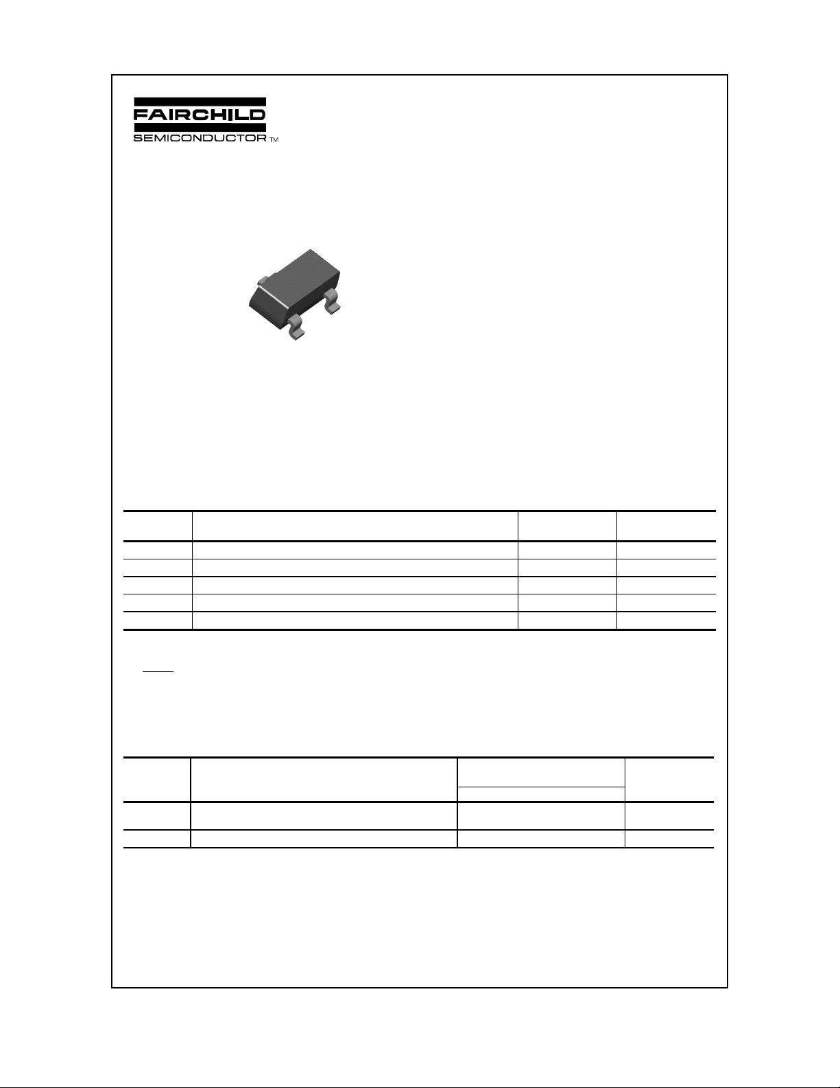
SOT-23
Mark: FD
B
PNP Darlington Transistor
This device is designed for applications requiring extremely high
current gain at currents to 800 mA. Sourced from Process 61.
Absolute Maximum Ratings* TA = 25°C unless otherwise noted
Symbol Parameter Value Units
V
CEO
V
CBO
V
EBO
I
C
TJ, T
stg
*These ratings are limiting values above which the serviceability of any semiconductor device may be impaired.
NOTES:
1) These ratings are based on a maximum junction temperature of 150 degrees C.
2) These are steady state limits. The factory should be consulted on applications involving pulsed or low duty cycle operations.
3) All voltages (V) and currents (A) are negative polarity for PNP transistors.
Collector-Emitt er Voltage 30 V
Collector-Base Voltage 40 V
Emitter-Base Voltage 10 V
Collector Current - Continuous 1.2 A
Operating and Stora ge Junction Temperature Range -55 to +150
C
°
3
Thermal Characteristics TA = 25°C unless otherwise noted
Symbol Characteristic Max Units
*BCV26
P
D
R
θ
JA
*Device mounted on FR-4 PCB 40 mm X 40 mm X 1.5 mm.
1997 Fairchild Semiconductor Corporation
Total Dev ice Dissipation
Derate above 25°C
Thermal Resistance , Junctio n to Ambient 357
350
2.8
mW
mW/°C
C/W
°

µ
µ
PNP Darlington Transistor
(continued)
Electrical Characteristics TA = 25°C unless otherwise noted
Symbol Parameter Test Conditions Min Typ Max Units
OFF CHARACTERISTICS
V
(BR)CEO
V
(BR)CBO
V
(BR)EBO
I
CBO
I
EBO
ON CHARACTERISTICS
h
FE
V
CE(
)
sat
V
sat
BE(
)
Collector-Emitt er Breakdo wn Volt age IC = 10 mA, IB = 0 30 V
Collector-Base Breakdown Voltage
= 10 µA, IE = 0
I
C
40 V
Emitter-Base Breakdown Voltage IE = 100 nA, IC = 0 10 V
Collector-Cutoff Current VCB = 30 V, IE = 0 0.1
Emitte r-Cutoff Current VEB = 10 V, IC = 0 0.1
DC Current Gain IC = 1.0 mA, VCE = 5.0 V
I
= 10 mA, VCE = 5.0 V
C
I
= 100 mA, VCE = 5.0 V
C
4,000
10,000
20,000
Collector-Emitter Saturation Voltage IC = 100 mA, IB = 0.1 mA 1.0 V
Base-Emitter Saturation Voltage IC = 100 mA, IB = 0.1 mA 1.5 V
BCV26
A
A
SMALL SIGNAL CHARACTERISTICS
f
T
C
C
NOTE: All voltages (V) and currents (A) are negative polarity for PNP transistors.
Current Gain - Bandwidth Product IC = 30 mA, VCE = 5.0 V,
f = 100 MHz
Collector Capacitance VCB = 30 V, IE = 0, f = 1.0 MHz 3.5 pF
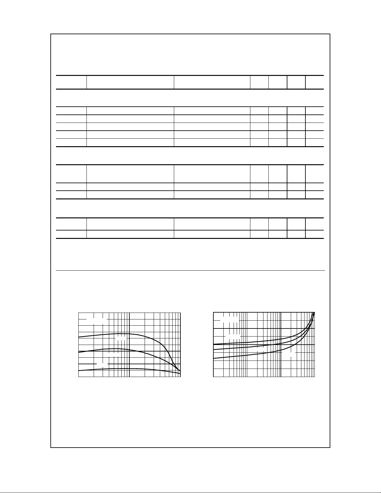
T ypical Characteristics
Typical Pulsed Cu rren t Gai n
vs Collector Curren t
50
V = 5V
40
30
20
10
FE
h - TYPICAL PUL S ED CU RREN T GAI N (K)
CE
125 °C
25 °C
- 40 °C
0
0.01 0.1 1
I - COLLECTOR CURRENT (A)
C
220 MHz
Co llector -Em itter Saturatio n
Voltag e vs Colle ctor Cur re nt
1.6
= 1000
β
1.2
- 40 °C
0.8
0.4
0
0.001 0.01 0.1 1
CES AT
V - COLLECTOR EMITTER VOLTAGE (V)
I - COLLECTOR CURRENT (A)
C
25 °C
125 °C

Typical Characteristics (continued)
BCV26
PNP Darlington T ransistor
(continued)
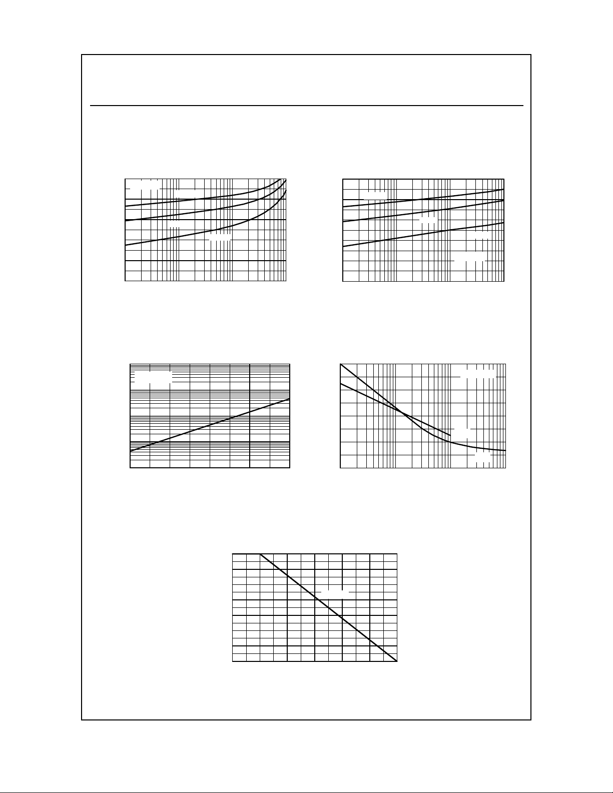
Bas e-Em itt er Sa turatio n
Volt a ge v s Colle c t or Cu rre nt
2
= 1000
β
1.6
1.2
0.8
0.4
BESAT
0
V - BASE EM ITTER VOLTAGE (V)
0.001 0.01 0.1 1
- 40 °C
25 °C
125 °C
I - COLLECTOR CURRENT (A)
C
Co llector-Cutoff Cur re nt
vs Amb ient Temp e r ature
100
V = 15V
CB
10
1
0.1
CBO
I - COLLECTOR CURRENT (nA)
0.01
25 50 75 100 125
T - AMBI E NT T E MP ERAT UR E ( C)
A
°
Base E mitter ON Voltage vs
Collector Curre nt
2
1.6
1.2
0.8
0.4
0
BE(ON)
0.001 0.01 0.1 1
V - BASE EMITTER ON VOLTAGE (V)
- 40 °C
25 °C
I - COLLECTOR CURRENT (A)
C
125 °C
V = 5V
CE
Inp u t a n d Output Capacitance
vs Reverse Bias Voltage
16
12
8
4
CAP ACITANCE ( pF)
0
0.1 1 10 100
REVER SE VO L TAGE (V)
f = 1.0 MHz
C
ib
C
3
ob
Power Dissipation vs
Ambient Temperature
350
300
250
200
150
100
50
D
P - POWER DISSIPATION (mW)
0
0 25 50 75 100 125 150
TEMPERATURE ( C)
SOT-23
o
 Loading...