BC857S
E2
B2
C1
BC857S
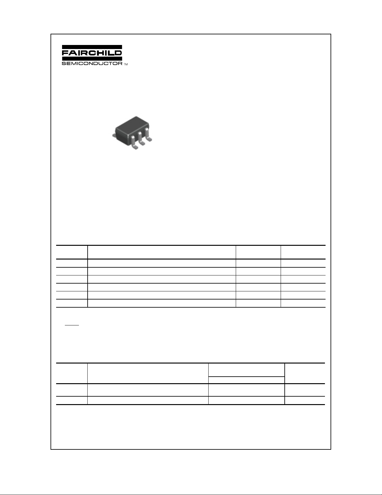
SC70-6
Mark: 3C
NOTE: The pinouts are symmetrical; pin 1 and pin
4 are interchangeable. Units inside the carrier can
be of either orientation and will not affect the
functionality of the device.
pin #1
C2
B1
E1
PNP Multi-Chip General Purpose Amplifier
This device is designed for general purpose amplifier applications at collector
currents to 200 mA. Sourced from Process 68.
Absolute Maximum Ratings* T
Symbol Parameter Value Units
V
CEO
V
CES
V
CBO
V
EBO
I
C
TJ, T
stg
*These ratings are limiting values above which the serviceability of any semiconductor device may be impaired.
NOTES:
1) These ratings are based on a maximum junction temperature of 150 degrees C.
2) These are steady state limits. The factory should be consulted on applications involving pulsed or low duty cycle operations.
3) All voltages (V) and currents (A) are negative polarity for PNP transistors.
Collector-Emitter Voltage 45 V
Collector-Base Voltage 50 V
Collector-Base Voltage 50 V
Emitter-Base V ol tage 5.0 V
Collector Current - Continuous 200 mA
Operating and Storage Junctio n Temperature Range -55 to +150
= 25°C unless otherwise noted
A
C
°
4
Thermal Characteristics T
= 25°C unless otherwise noted
A
Symbol Characteristic Max Units
BC857S
P
D
R
JA
θ
1998 Fairchild Semiconductor Corporation
Total Device Dissipation
Derate above 25°C
300
2.4
Thermal Resistance, Junction to Ambient 415
mW
mW/°C
C/W
°

PNP Multi-Chip General Purpose Amplifier
(continued)
BC857S
Electrical Characteristics T
= 25°C unless otherwise noted
A
Symbol Parameter Test Conditions Min Typ Max Units
OFF CHARACTERISTICS
V
(BR)CEO
V
(BR)CES
V
(BR)CBO
V
(BR)EBO
I
CBO
Collector-Emitter Break down Voltage IC = 10 mA, IB = 0 45 V
Collector-Base Breakdown Volt age
Collector-Base Breakdown Volt age
Emitter-Base Breakdown Voltage
I
= 10 µA, IE = 0
C
I
= 10 µA, IE = 0
C
I
= 10 µA, IC = 0
E
Collector-Cutoff Current VCB = 30 V
V
= 30 V, TA = 150°C
CB
50 V
50 V
5.0 V
15
4.0
nA
µ
ON CHARACTERISTICS
h
V
V
FE
sat
CE(
BE(on)
DC Current Gain IC = 2.0 mA, VCE = 5.0 V 125 630
Collector-Emitter S aturation Voltage IC = 10 mA, IB = 0.5 mA
)
Base-Emitter On Volt age IC = 2.0 mA, VCE = 5.0 V
= 100 mA, IB = 5.0 mA
I
C
= 10 mA, VCE = 5.0 V
I
C
0.6 0.75
0.3
0.65VV
0.82VV
SMALL SIGNAL CHARACTERISTICS
f
T
C
obo
Current Gain - Bandwidth Product IC = 10 mA, VCE = 5.0,
f = 100 mHz
Output Capacitance VCB = 10 V, f = 1.0 MHz 3.5 pF
NF Noise Figure IC = 0.2 mA, VCE = 5.0,
= 2.0 kΩ, f = 1.0 kHz,
R
S
BW = 200 Hz
NOTE: All voltages (V) and currents (A) are negative polarity for PNP transistors.
200 MHz
2.5 dB
A
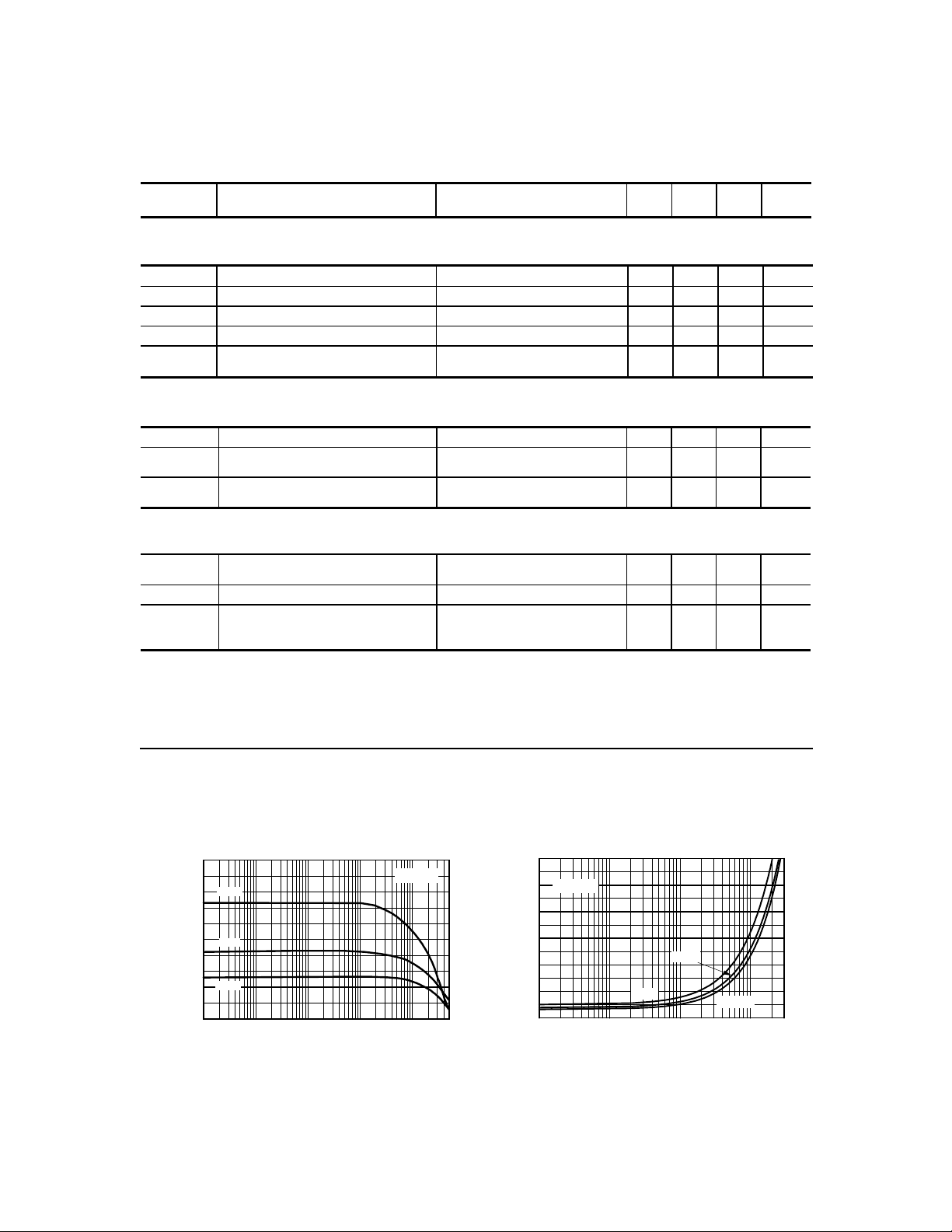
T ypical Characteristics
Typical Pulsed Current Gain
vs Collector Current
500
125 °C
400
300
25 °C
200
- 40 °C
100
0
FE
0.01 0.1 1 10 100
h - TYPICAL PULSED CURRENT GAIN
I - COLLECTOR CURRENT (mA)
C
V = 5V
CE
Co llector-Em itt er Saturatio n
Voltage vs Coll ector Cur re nt
0.3
0.25
β
= 10
0.2
0.15
125 °C
25 °C
- 40 °C
0.1
0.05
0
0.1 1 10 100 300
CES AT
V - COL LECTOR EM ITTER VOLTAGE ( V)
I - COLLECTOR CURRE NT (mA)
C
 Loading...