April 2014
BAV99
200 mA 70 V High Conductance Ultra-Fast Switching
Diode
BAV99 — 200 mA 70 V High Conductance Ultra-Fast Switching Diode
Features
• High Conductance: IF = 200 mA
• Fast Switching Speed: t
• Small Plastic SOT-23 Package
• Series-Pair Configuration
< 6 ns Maximum
rr
Applications
• High-Speed Switching Applications
3
2
1
SOT-23
Description
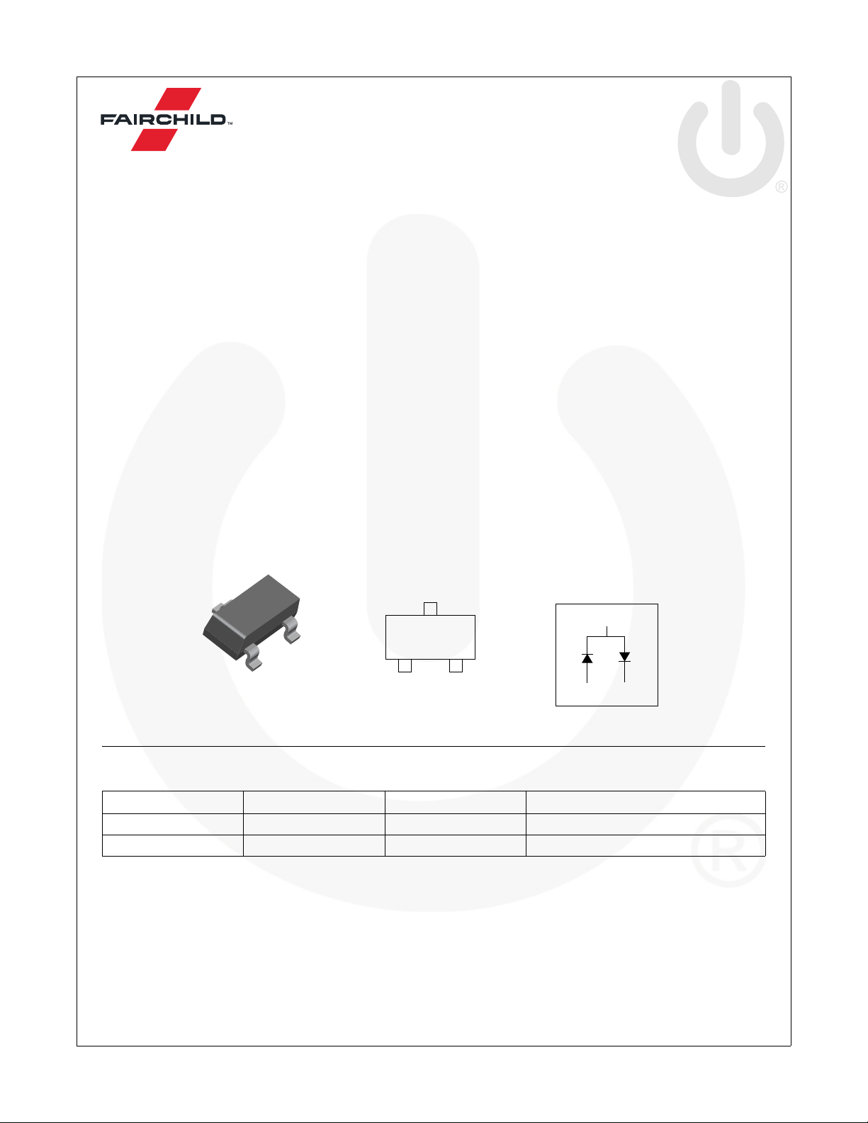
The BAV99 is a 350 mW high-speed switching diode
array with series-pair diode configuration. It achieves
high-current conductivity, up to 200 mA, in a very small
2
footprint. These features make the BAV99 optimal
7mm
for area-constrained applications that need a little extra
power capability.
For common cathode and common anode high-speed
switching diodes, explore Fairchild's BAV70 and BAW56.
Looking for more options in the SOT-23 package? Check
Fairchild's MMBD family.
Connection Diagram
3
3
A7
12
2
1
Ordering Information
Part Number Marking Package Packing Method
BAV99 A7 SOT-23 3L Tape and Reel, Reel 7 inch
BAV99_D87Z A7 SOT-23 3L Tape and Reel, Reel 13 inch
© 2001 Fairchild Semiconductor Corporation www.fairchildsemi.com
BAV99 Rev. 1.1.0 1

BAV99 — 200 mA 70 V High Conductance Ultra-Fast Switching Diode
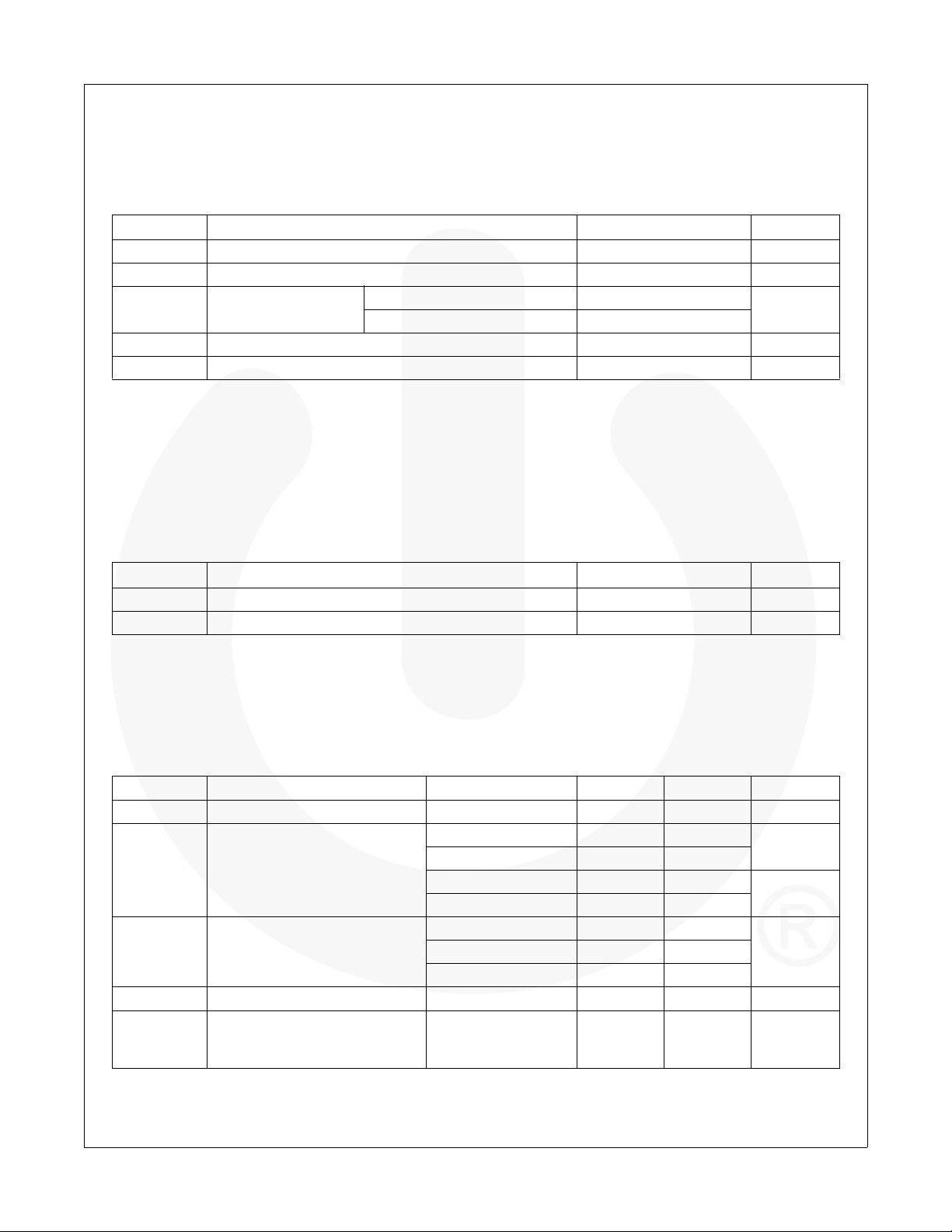
Absolute Maximum Ratings
(1)
Stresses exceeding the absolute maximum ratings may damage the device. The device may not function or be operable above the recommended operating conditions and stressing the parts to these levels is not recommended. In addition, extended exposure to stresses above the recommended operating cond itions may affect device reliability. The
absolute maximum ratings are stress ratings only. Values are at T
= 25°C unless otherwise noted.
A
Symbol Parameter Value Unit
V
RRM
I
F(AV)
I
FSM
T
STG
T
J
Note:
1. These ratings are based on a maximum junction temperature of 150°C.
These are steady-state limits. Fairchild Semiconductor should be consulted on applications involving pulsed
or low-duty cycle operations.
Thermal Characteristics
V a lues are at TA = 25°C unless otherwise noted.
Maximum Repetitive Reverse Voltage 70 V
Average Rectified Forward Current 200 mA
Non-Repetitive Peak
Forward Surge Current
Pulse Width = 1.0 Second 1.0
Pulse Width = 300 Microseconds 8.0
A
Storage Temperature Range -55 to +150 °C
Operating Junction T emperature Range -55 to +150 °C
(2)
Symbol Parameter Value Unit
P
D
R
θJA
Note:
2. PCB size: FR-4, 76 mm x 114 mm x 1.57 mm (3.0 inch x 4.5 inch x 0.062 inch) with minimum land pattern size.
Power Dissipation 350 mW
Thermal Resistance, Junction to Ambient 357 °C/W
Electrical Characteristics
V a lues are at TA = 25°C unless otherwise noted.
Symbol Parameter Conditions Min. Max. Unit
V
R
V
F
I
R
C
T
t
rr
Breakdown Voltage, per Diode IR = 100 μA70 V
Forward Voltage, per Diode
Reverse Leakage, per Diode
IF = 1 mA 715
I
= 10 mA 855
F
= 50 mA 1.00
I
F
I
= 150 mA 1.25
F
V
= 70 V 2.5
R
= 25 V, TA = 150°C30.0
R
= 70 V, TA = 150°C50.0
V
R
mV
V
μAV
Total Capacitance, per Diode VR = 0 V, f = 1.0 MHz 1.5 pF
= IR = 10 mA,
I
Reverse-Recovery Time,
per Diode
F
= 1 mA,
I
RR
R
= 100 Ω
L
6.0 ns
© 2001 Fairchild Semiconductor Corporation www.fairchildsemi.com
BAV99 Rev. 1.1.0 2

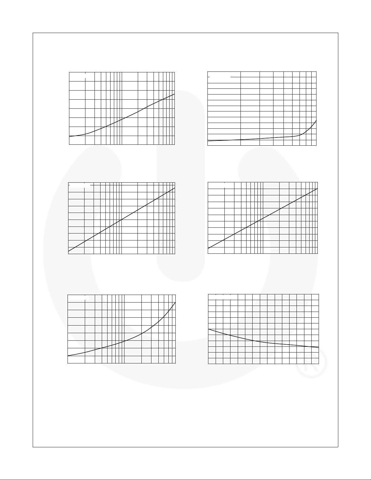
Typical Performance Characteristics
110
120
130
140
150
1 2 3 5 10 20 30 50 100
Ta= 25 C
Reverse Voltage, V
R
[V]
Reverse Current, IR [uA]
°
0
50
100
150
200
250
300
10 20 3 0 5 0 70 100
Ta= 25 C
Reverse Current, I
R
[nA]
Reverse Voltage, V
[V
]
°
250
300
350
400
450
1 2 3 5 1 0 20 30 50 100
Ta= 25 C
Forward Voltage, V
F
[mV]
Forward Current, I
[uA
]
°
450
500
550
600
650
700
0.1 0 .2 0.3 0 .5 1 2 3 5 10
Ta= 25 C
Forward Voltage, V
F
[mV]
Forward Current, I
[mA
]
°
0.6
0.8
1.0
1.2
1.4
10 20 3 0 50 1 00 200 300 500
Ta= 25 C
Forward Voltage, V
F
[V]
Forward C urrent, I
[mA ]
°
02468101214
1.0
1.1
1.2
1.3
Ta= 25 C
Total Capacitance [pF]
Reverse Voltage [V]
°
BAV99 — 200 mA 70 V High Conductance Ultra-Fast Switching Diode
Figure 1. Reverse Voltage vs. Reverse Current
Figure 3. Forward Voltage vs. Forward Current
V
- 1 to 100 μA
F
Figure 2. Reverse Current vs. Reverse Voltage
Figure 4. Forward Voltage vs. Forward Current
V
- 0.1 to 10 mA
F
Figure 5. Forward Voltage vs. Forward Current
V
© 2001 Fairchild Semiconductor Corporation www.fairchildsemi.com
BAV99 Rev. 1.1.0 3
- 10 to 800 mA
F
Figure 6. Total Capacitance vs. Reverse Voltage
 Loading...