Fairchild 54F138, 74F138 service manual

查询54F138供应商
54F/74F138
1-of-8 Decoder/Demultiplexer
54F/74F138 1-of-8 Decoder/Demultiplexer
November 1994
General Description
The ’F138 is a high-speed 1-of-8 decoder/demultiplexer.
This device is ideally suited for high-speed bipolar memory
chip select address decoding. The multiple input enables
allow parallel expansion to a 1-of-24 decoder using just
three ’F138 devices or a 1-of-32 decoder using four ’F138
devices and one inverter.
Commercial Military
74F138PC N16E 16-Lead (0.300×Wide) Molded Dual-In-Line
54F138DM (Note 2) J16A 16-Lead Ceramic Dual-In-Line
74F138SC (Note 1) M16A 16-Lead (0.150×Wide) Molded Small Outline, JEDEC
74F138SJ (Note 1) M16D 16-Lead (0.300×Wide) Molded Small Outline, EIAJ
54F138FM (Note 2) W16A 16-Lead Cerpack
54F138LM (Note 2) E20A 20-Lead Ceramic Leadless Chip Carrier, Type C
Note 1: Devices also available in 13×reel. Use suffixeSCX and SJX.
Note 2: Military grade device with environmental and burn-in processing. Use suffix
Package
Number
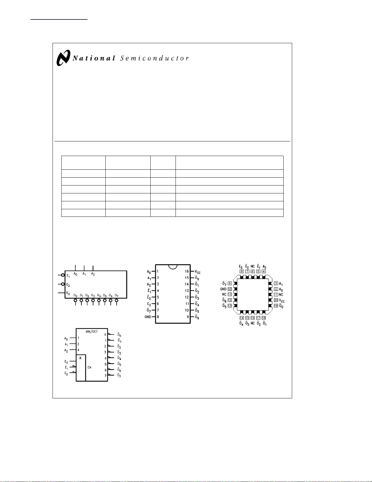
Logic Symbols
Pin Assignment for DIP,
SOIC and Flatpak
Features
Y
Demultiplexing capability
Y
Multiple input enable for easy expansion
Y
Active LOW mutually exclusive outputs
Y
Guaranteed 4000V minimum ESD protection
Package Description
e
DMQB, FMQB and LMQB.
Connection Diagrams
Pin Assignment
for LCC
TL/F/9478– 3
IEEE/IEC
TL/F/9478– 6
TRI-STATEÉis a registered trademark of National Semiconductor Corporation.
C
1995 National Semiconductor Corporation RRD-B30M75/Printed in U. S. A.
TL/F/9478
TL/F/9478– 1
TL/F/9478– 2

Unit Loading/Fan Out
54F/74F
Pin Names Description
A0–A
E
1,E2
E
3
O0–O
Address Inputs 1.0/1.0 20 mA/b0.6 mA
2
Enable Inputs (Active LOW) 1.0/1.0 20 mA/b0.6 mA
Enable Input (Active HIGH) 1.0/1.0 20 mA/b0.6 mA
Outputs (Active LOW) 50/33.3
7
U.L. Input I
HIGH/LOW Output IOH/I
IH/IIL
b
1 mA/20 mA
OL
Functional Description
The ’F138 high-speed 1-of-8 decoder/demultiplexer accepts three binary weighted inputs (A
enabled, provides eight mutually exclusive active LOW outputs (O
active LOW (E
will be HIGH unless E
This multiple enable function allows easy parallel expansion
). The ’F138 features three Enable inputs, two
0–O7
) and one active HIGH (E3). All outputs
1,E2
and E2are LOW and E3is HIGH.
1
0,A1,A2
) and, when
of the device to a 1-of-32 (5 lines to 32 lines) decoder with
just four ’F138 devices and one inverter (See
’F138 can be used as an 8-output demultiplexer by using
one of the active LOW Enable inputs as the data input and
the other Enable inputs as strobes. The Enable inputs which
are not used must be permanently tied to their appropriate
active HIGH or active LOW state.
Truth Table
Inputs Outputs
E1E2E3A0A
HXXXXXHH H HHHHH
XHXXXXHH H HHHHH
XXLXXXHH H HHHHH
LLHLLL L H HHHHHH
LLHHLLHL H HHHHH
LLHLHLHH L HHHHH
LLHHHLHH H LHHHH
LLHLLHHHH H LHHH
LLHHLHHHHHHLHH
LLHLHHHHH HHH LH
LLHHHHHHH HHHHL
HeHIGH Voltage Level
e
L
LOW Voltage Level
e
X
Immaterial
A2O0O1O
1
O3O4O5O6O
2
Figure 1
). The
7
2

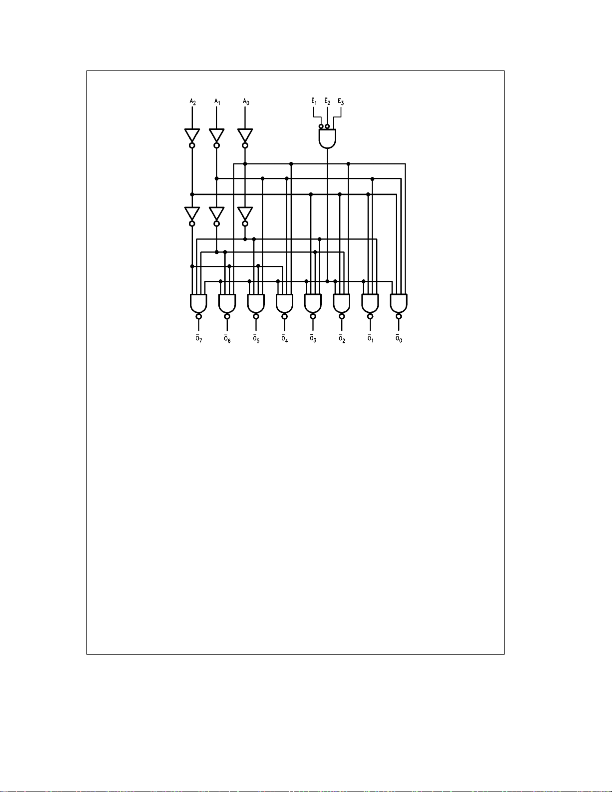
Logic Diagram
Please note that this diagram is provided only for the understanding of logic operations and should not be used to estimate propagation delays.
TL/F/9478– 4
3
 Loading...