

Fairchild 54F132, 74F132 service manual
查询54F132DM供应商
November 1994
54F/74F132
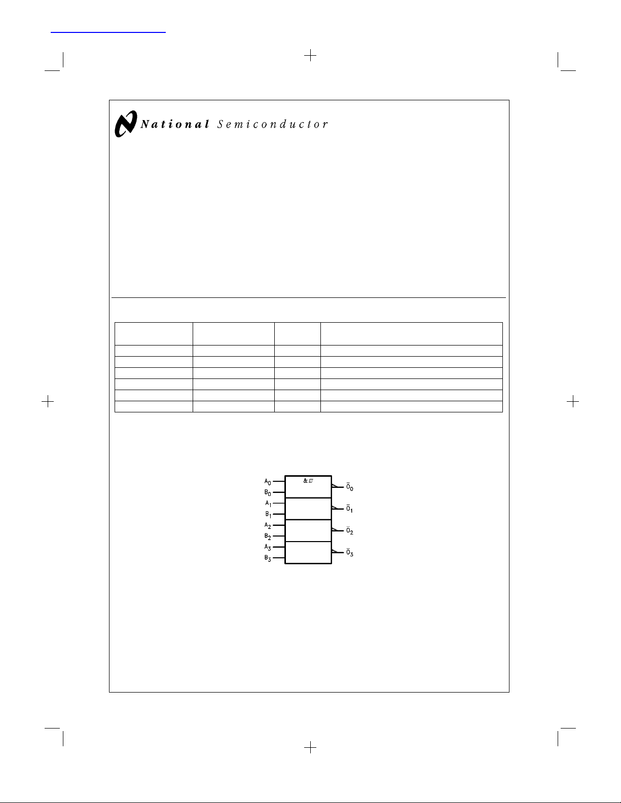
Quad 2-Input NAND Schmitt Trigger
General Description
The ’F132 contains four 2-input NAND gates which accept
standard TTL input signals and provide standard TTL output
levels. They are capable of transforming slowly changing input signals into sharply defined, jitter-free output signals. In
addition, they haveagreater noise margin than conventional
NAND gates.
Each circuit contains a 2-input Schmitt trigger followed by
level shifting circuitry and a standard FAST
ture. The Schmitt trigger uses positive feedback to effectively
speed-up slow input transitions, and provide different input
®
output struc-
Ordering Code: See Section 0
Commercial Military Package Package Description
Number
74F132PC N14A 14-Lead (0.300" Wide) Molded Dual-In-Line
54F132DM (Note 2) J14A 14-Lead Ceramic Dual-In-Line
74F132SC (Note 1) M14A 14-Lead (0.150" Wide) Molded Small Outline, JEDEC
74F132SJ (Note 1) M14D 14-Lead (0.300" Wide) Molded Small Outline, EIAJ
54F132FM (Note 2) W14B 14-Lead Cerpack
54F132LM (Note 2) E20A 20-Lead Ceramic Leadless Chip Carrier, Type C
Note 1: Devices also available in 13" reel. Use suffix=SCX and SJX.
Note 2: Military grade device with environmental and burn-in processing. Use suffix=DMQB, FMQB and LMQB.
Logic Symbol
threshold voltages for positive and negative-going transitions. This hysteresis between the positive-going and
negative-going input threshold (typically 800 mV) is determined by resistor ratios and is essentially insensitive to temperature and supply voltage variations.
Features
n Guaranteed 4000V minimum ESD protection
n Standard Military Drawing (SMD)
n 5962-89487
54F/74F132 Quad 2-Input NAND Schmitt Trigger
54F/74F132
DSXXX
IEEE/IEC
DS009477-3
TRI-STATE®is a registered trademark of National Semiconductor Corporation.
© 1997 National Semiconductor Corporation DS009477 www.national.com
1
PrintDate=1997/08/28 PrintTime=12:25:28 10193 ds009477 Rev. No. 1 cmserv
Proof 1
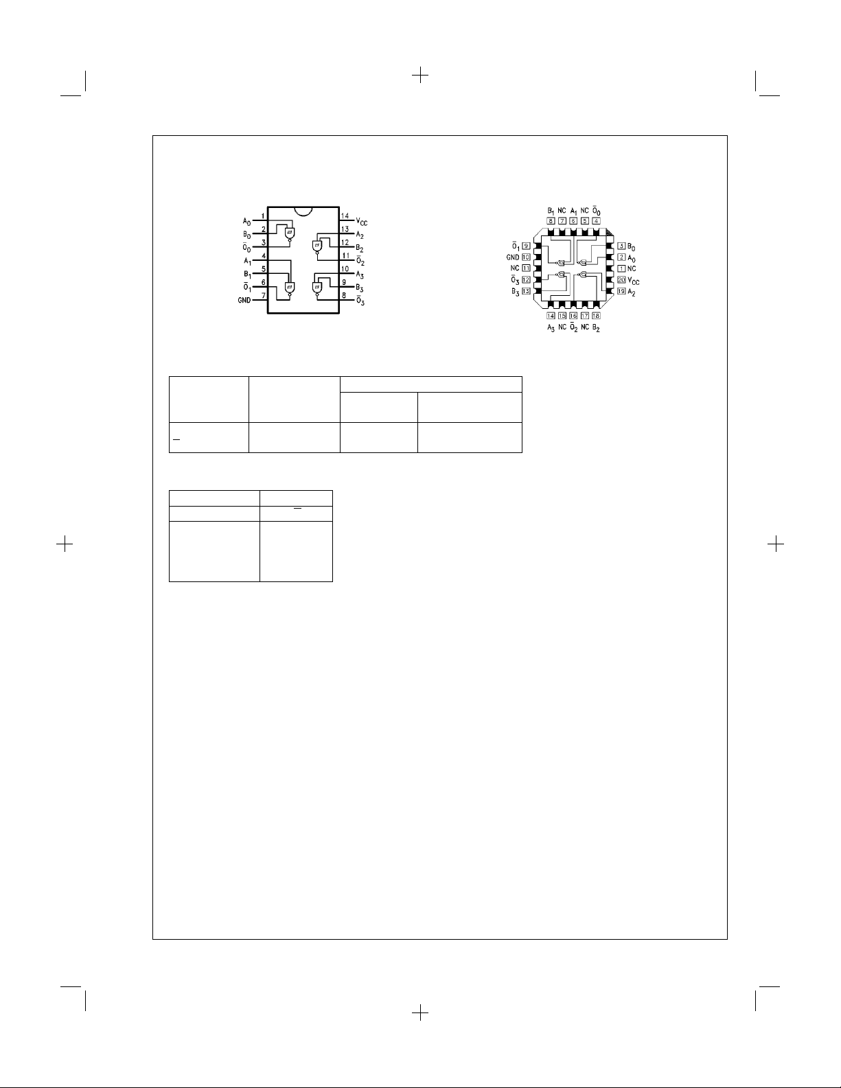
Connection Diagrams
Pin Assignment for
DIP, SOIC and Flatpak
DS009477-1
Unit Loading/Fan Out
See Section 0 for U.L. definitions
54F/74F
Pin Names Description U.L. Input I
HIGH/LOW Output IOH/I
An,B
O
n
n
Inputs 1.0/1.0 20 µA/−0.6 mA
Outputs 50/33.3 −1 mA/20 mA
Function Table
Inputs Outputs
AB O
LL H
LH H
HL H
HH L
=
H
HIGH Voltage Level
L=LOW Voltage Level
Pin Assignment
for LCC
DS009477-2
DSXXX
IH/IIL
OL
www.national.com 2
PrintDate=1997/08/28 PrintTime=12:25:31 10193 ds009477 Rev. No. 1 cmserv Proof 2
Absolute Maximum Ratings (Note 3)
If Military/Aerospace specified devices are required,
please contact the National Semiconductor Sales Office/
Current Applied to Output
in LOW State (Max) twice the rated I
ESD Last Passing Voltage (Min) 4000V
Distributors for availability and specifications.
Storage Temperature −65˚C to +150˚C
Ambient Temperature under Bias −55˚C to +125˚C
Junction Temperature under Bias −55˚C to +175˚C
Plastic −55˚C to +150˚C
Pin Potential to
V
CC
Ground Pin −0.5V to +7.0V
Input Voltage (Note 4) −0.5V to +7.0V
Input Current (Note 4) −30 mA to +5.0 mA
Voltage Applied to Output
=
in HIGH State (with V
0V)
CC
Standard Output −0.5V to V
TRI-STATE®Output −0.5V to +5.5V
Recommended Operating
Conditions
Free Air Ambient Temperature
Military −55˚C to +125˚C
Commercial 0˚C to +70˚C
Supply Voltage
Military +4.5V to +5.5V
Commercial +4.5V to +5.5V
Note 3: Absolute maximum ratings are values beyond which the device may
be damaged or have its useful life impaired. Functional operation under these
conditions is not implied.
CC
Note 4: Either voltage limit or current limit is sufficient to protect inputs.
DC Electrical Characteristics
Symbol Parameter 54F/74F Units V
Min Typ Max
V
V
∆V
V
V
V
I
I
I
V
I
I
I
I
I
T+
T−
CD
OH
OL
IH
BVI
CEX
ID
OD
IL
OS
CCH
CCL
Positive-going Threshold 1.5 2.0 V 5.0
Negative-going Threshold 0.7 1.1 V 5.0
+
T
Hysteresis (V
−
−V
) 0.4 V 5.0
T
T
Input Clamp Diode Voltage −1.2 V Min I
Output HIGH 54F 10%V
Voltage 74F 10%V
74F 5%V
Output LOW 54F 10%V
Voltage 74F 10%V
2.5 I
CC
2.5 V Min I
CC
2.7 I
CC
CC
CC
0.5 V Min I
0.5 I
Input HIGH 54F 20.0 µA Max V
Current 74F 5.0
Input HIGH Current 54F 100 µA Max V
Breakdown Test 74F 7.0
Output HIGH 54F 250 µA Max V
Leakage Current 74F 50
Input Leakage 74F 4.75 V 0.0 I
Test All Other Pins Grounded
Output Leakage 74F 3.75 µA 0.0 V
Circuit Current All Other Pins Grounded
Input LOW Current −0.6 mA Max V
Output Short-Circuit Current −60 −150 mA Max V
Power Supply Current 17.0 mA Max V
Power Supply Current 18.0 mA Max V
(mA)
OL
IN
OH
OH
OH
OL
OL
IN
IN
OUT
ID
IOD
IN
OUT
O
O
=
−18 mA
=
−1 mA
=
−1 mA
=
−1 mA
=
20 mA
=
20 mA
=
2.7V
=
7.0V
=
=
1.9 µA
=
=
0.5V
=
=
HIGH
=
LOW
150 mV
Conditions
V
CC
0V
CC
3 www.national.com
PrintDate=1997/08/28 PrintTime=12:25:38 10193 ds009477 Rev. No. 1 cmserv Proof 3
 Loading...