

Fairchild 54F109, 74F109 service manual
查询54F109DM供应商
54F/74F109
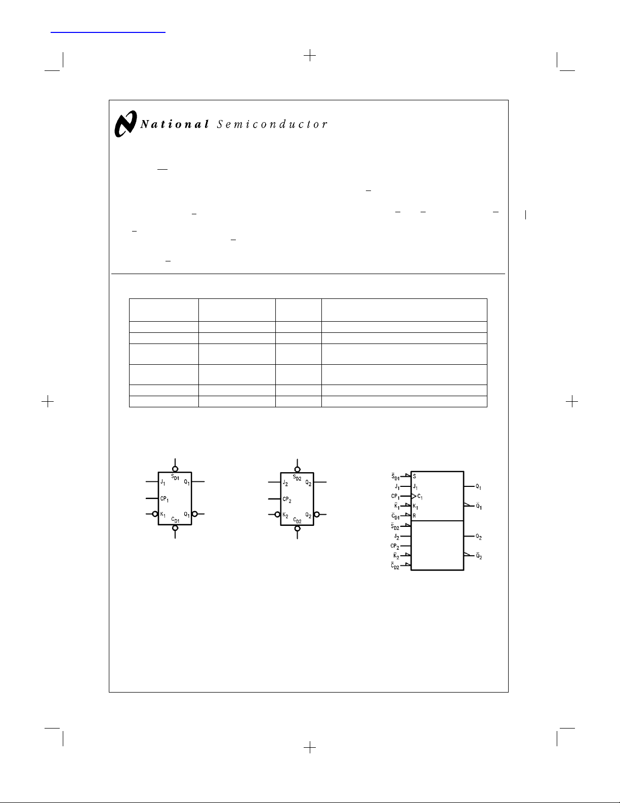
Dual JK Positive Edge-Triggered Flip-Flop
General Description
The ’F109 consists of two high-speed, completely independent transition clocked JK flip-flops. The clocking operation
is independent of rise and fall times of the clock waveform.
The JKdesign allows operation as a D flip-flop (refer to ’F74
data sheet) by connecting the J and K inputs.
Asynchronous Inputs:
LOW input to S
sets Q to HIGH level
D
Ordering Code: See Section 0
Commercial Military Package Package Description
Number
74F109PC N16E 16-Lead (0.300" Wide) Molded Dual-in-Line
54F109DM (Note 2) J16A 16-Lead Ceramic Dual-in-Line
74F109SC (Note 1) M16A 16-Lead (0.150" Wide) Molded Small Outline,
74F109SJ (Note 1) M16D 16-Lead (0.300" Wide) Molded Small Outline,
54F109FM (Note 2) W16A 16-Lead Cerpack
54F109LM (Note 2) E20A 16-Lead Ceramic Leadless Chip Carrier, Type C
Note 1: Devices also available in 13" reel. Use suffix=SCX and SJX.
Note 2: Military grade device with environmental and burn-in processing. Use suffix=DMQB, FMQB and LMQB.
Logic Symbols
LOW input to CDsets Q to LOW level
Clear and Set are independent of clock
Simultaneous LOW on C
HIGH
and SDmakes both Q and Q
D
Features
n Guaranteed 4000V minimum ESD protection.
JEDEC
EIAJ
November 1994
54F/74F109 Dual JK Positive Edge-Triggered Flip-Flop
DSXXX
54F/74F109
IEEE/IEC
DS009471-3
FAST®and TRI-STATE®are registered trademarks of National Semiconductor Corporation.
© 1997 National Semiconductor Corporation DS009471 www.national.com
DS009471-4
DS009471-6
1
PrintDate=1997/08/28 PrintTime=11:45:22 10182 ds009471 Rev. No. 1 cmserv
Proof 1
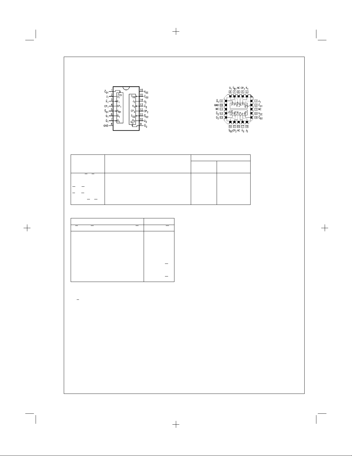
Connection Diagrams
Pin Assignment
for DIP, SOIC and Flatpak
DS009471-1
Pin Assignment
for LCC
Unit Loading/Fan Out
See Section 0 for U.L. definitions
54F/74F
Pin Names Description U.L. Input I
HIGH/LOW Output IOH/I
J1,J2,K1,K
CP
,CP
1
2
C
D1,CD2
S
D1,SD2
Q
1,Q2,Q1,Q2
Data Inputs 1.0/1.0 20 µA/−0.6 mA
2
Clock Pulse Inputs (Active Rising Edge) 1.0/1.0 20 µA/−0.6 mA
Direct Clear Inputs (Active LOW) 1.0/3.0 20 µA/−1.8 mA
Direct Set Inputs (Active LOW) 1.0/3.0 20 µA/−1.8 mA
Outputs 50/33.3 −1 mA/20 mA
Truth Table
Inputs Outputs
S
C
D
LHXXXHL
HLXXXLH
LLXXXHH
HH
HH
HH
HH
HHLXXQ
H (h)=HIGH Voltage Level
L (l)=LOW Voltage Level
=
N
LOW-to-HIGH Transition
X=Immaterial
)=Before LOW-to-HIGH Transition of Clock
Q
0(Q0
Lower case letters indicate the state of the referenced output one setup time prior to the LOW-to-HIGH clock transition.
CP J K QQ
D
N
llLH
N
h l Toggle
N
lhQ0Q
N
hhH L
0
0
Q
0
DS009471-2
DSXXX
IH/IIL
OL
www.national.com 2
PrintDate=1997/08/28 PrintTime=11:45:23 10182 ds009471 Rev. No. 1 cmserv Proof 2
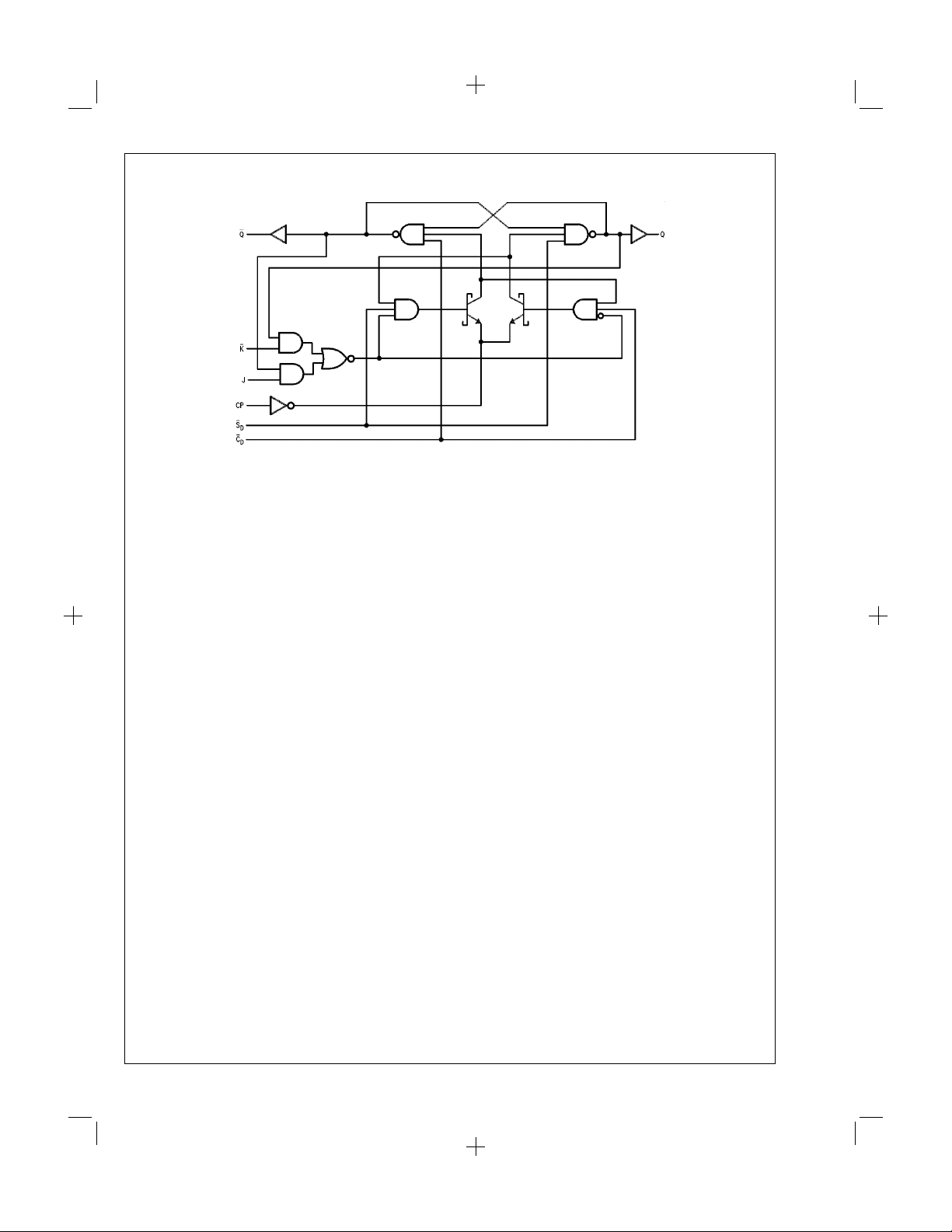
Logic Diagram (One Half Shown)
Please note that this diagram is provided only for the understanding of logic operations and should not be used to estimate propagation delays.
DS009471-5
3 www.national.com
PrintDate=1997/08/28 PrintTime=11:45:24 10182 ds009471 Rev. No. 1 cmserv Proof 3
 Loading...