Fairchild 5497, DM7497 service manual

查询5497供应商
5497/DM7497
Synchronous Modulo-64 Bit Rate Multiplier
General Description
The ’97 contains a synchronous 6-stage binary counter and
six decoding gates that serve to gate the clock through to
the output at a sub-multiple of the input frequency. The output pulse rate, relative to the clock frequency, is determined
by signals applied to the Select (S0 –S5) inputs. Both true
and complement outputs are available, along with an enable
input for each. A Count Enable input and a Terminal Count
output are provided for cascading two or more packages.
An asynchronous Master Reset input prevents counting and
resets the counter.
5497/DM7497 Synchronous Modulo-64 Bit Rate Multiplier
June 1989
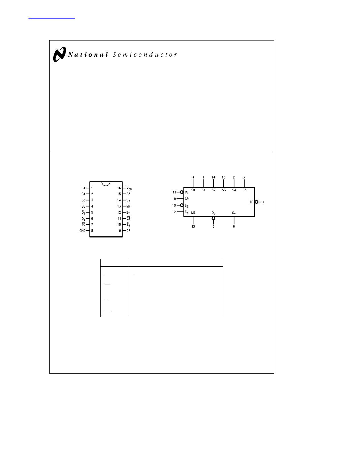
Connection Diagram
Dual-In-Line Package
Order Number 5497DMQB, 5497FMQB or DM7497N
See NS Package Number J16A, N16E or W16A
Pin Names Description
S0–S5 Rate Select Inputs
E
Z
E
Y
CE
CP Clock Pulse Input (Active Rising Edge)
MR Asynchronous Master Reset Input (Active HIGH)
O
Z
O
y
TC
OZEnable Input (Active LOW)
OYEnable Input
Count Enable Input (Active LOW)
Gated Clock Output (Active LOW)
Complement Output (Active HIGH)
Terminal Count Output (Active LOW)
TL/F/9780– 1
Logic Symbol
V
CC
GND
e
e
Pin 16
Pin 8
TL/F/9780– 2
C
1995 National Semiconductor Corporation RRD-B30M115/Printed in U. S. A.
TL/F/9780

Absolute Maximum Ratings (Note)
The ‘‘Absolute Maximum Ratings’’ are those values
If Military/Aerospace specified devices are required,
please contact the National Semiconductor Sales
Office/Distributors for availability and specifications.
Supply Voltage 7V
Input Voltage 5.5V
Operating Free Air Temperature Range
54
DM74 0
Storage Temperature Range
b
55§Ctoa125§C
Ctoa70§C
§
b
65§Ctoa150§C
Note:
beyond which the safety of the device cannot be guaranteed. The device should not be operated at these limits. The
parametric values defined in the ‘‘Electrical Characteristics’’
table are not guaranteed at the absolute maximum ratings.
The ‘‘Recommended Operating Conditions’’ table will define
the conditions for acutual device operation.
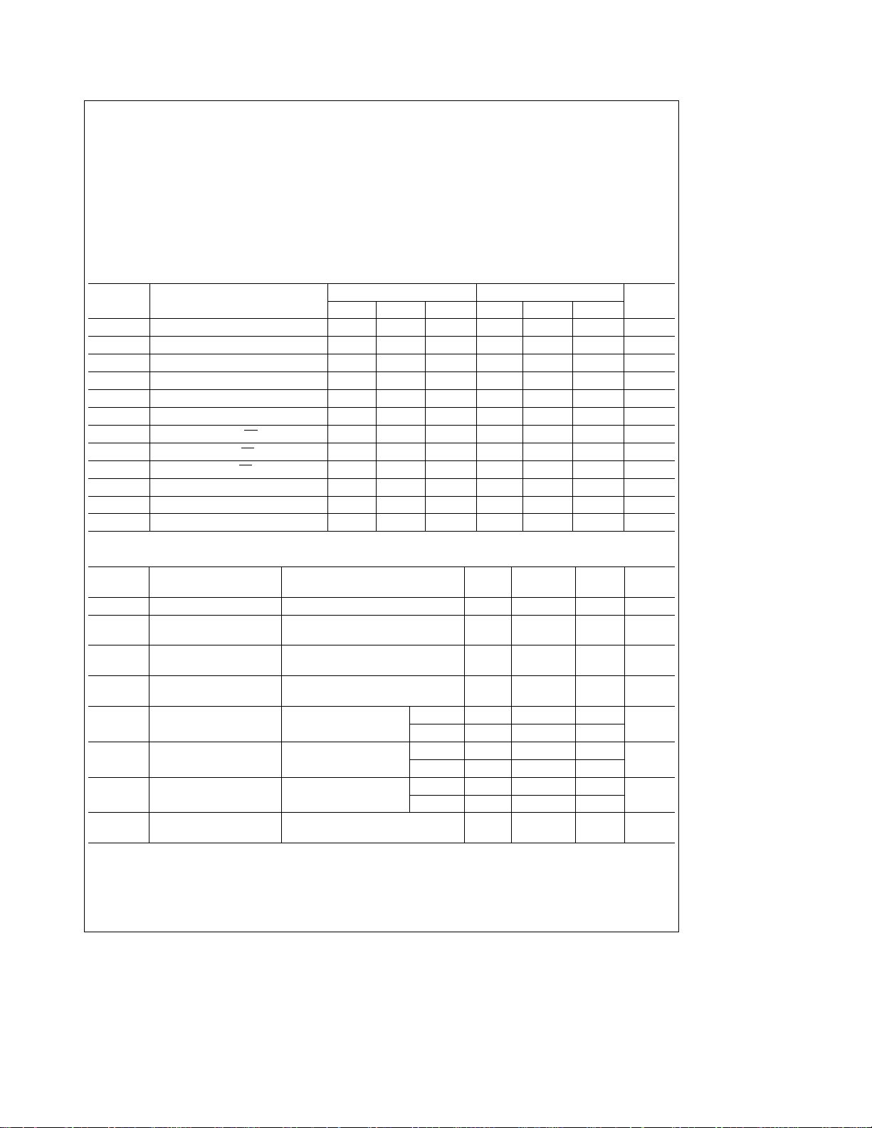
Recommended Operating Conditions
Symbol Parameter
V
CC
V
IH
V
IL
I
OH
I
OL
T
A
Supply Voltage 4.5 5 5.5 4.75 5 5.25 V
High Level Input Voltage 2 2 V
Low Level Input Voltage 0.8 0.8 V
High Level Output Current
Low Level Output Current 16 16 mA
Free Air Operating Temperature
Min Nom Max Min Nom Max
b
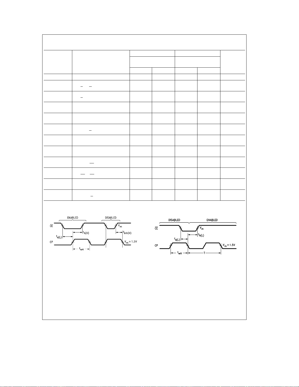
ts(L) Setup Time LOW, CE to CP Rising 25 25 ns
th(H) Hold Time HIGH, CE to CP Rising 0 0 ns
th(L) Hold Time LOW, CE to CP Falling 0 0 ns
tw(H) CP Pulse Width HIGH 20 20 ns
tw(L) CP Pulse Width LOW 20 ns
tw(H) MR Pulse Width HIGH 15 15 ns
5497 DM7497
b
0.4
b
55 125 0 70
Units
0.4 mA
C
§
Electrical Characteristics Over recommended operating free air temperature range (unless otherwise noted)
Symbol Parameter Conditions Min
e
V
I
V
OH
V
OL
I
I
I
IH
I
IL
I
OS
I
CC
Input Clamp Voltage V
High Level Output V
Voltage V
Low Level Output V
Voltage V
Input Current@Max V
Input Voltage
High Level Input Current V
Low Level Input Current V
Short Circuit V
Output Current (Note 2)
Supply Current With V
Outputs High
CC
CC
e
IL
CC
e
IH
CC
CC
Clock Inputs
CC
Clock Inputs
CC
CC
eb
Min, I
e
Min, I
Max
e
Min, I
Min
e
Max, V
e
Max, V
e
Max, V
e
Max 54
e
Max
12 mA
I
e
Max,
OH
e
Max,
OL
e
5.5V
I
e
2.4V DM74 40
I
e
0.4V DM74
I
2.4 3.4 V
54 80
54
b
DM74
b
2
20
18
Typ
(Note 1)
Max Units
b
1.5 V
0.2 0.4 V
1mA
b
1.6
b
3.2
b
55
b
55
120 mA
mA
mA
mA

Switching Characteristics
ea
V
CC
5.0V, T
ea
25§C (See Section 1 for waveforms and load configurations)
A
Symbol Parameter
f
t
t
t
t
t
t
t
t
t
t
t
t
t
t
t
t
t
t
t
t
max
PLH
PHL
PLH
PHL
PLH
PHL
PLH
PHL
PLH
PHL
PLH
PHL
PLH
PHL
PLH
PHL
PLH
PHL
PLH
PHL
Maximum Clock Frequency 25 25 MHz
Propagation Delay 18 18
EZto O
Z
Propagation Delay 30 30
EZto O
Y
Propagation Delay 14 14
EYto O
Y
Propagation Delay 23 23
Snto O
Y
Propagation Delay 14 14
Snto O
Z
Propagation Delay 39 39
CP to O
Y
Propagation Delay 18 18
CP to O
Z
Propagation Delay 35 30
CP to TC 33 33
Propagation Delay 25 20
CE to TC 21 21
Propagation Delay
MR to O
Y
Propagation Delay
MR to O
Z
5497 DM7497
e
15 pF C
C
L
e
R
400X R
L
e
15 pF
L
e
400X
L
Min Max Min Max
23 23
33 33
10 10
23 23
14 14
30 30
26 26
43 36 ns
34 23 ns
Units
ns
ns
ns
ns
ns
ns
ns
ns
ns
Timing Diagrams
TL/F/9780– 5
TL/F/9780– 6
3
 Loading...