

October 2007
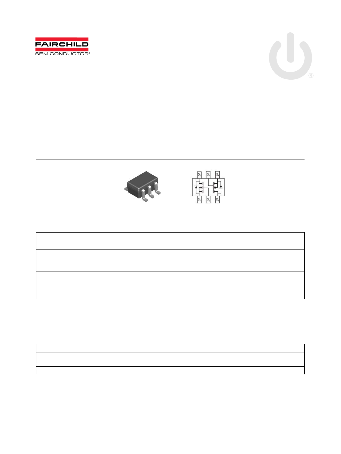
2N7002DW
N-Channel Enhancement Mode Field Effect Transistor
Features
• Dual N-Channel MOSFET
• Low On-Resistance
• Low Gate Threshold Voltage
• Low Input Capacitance
• Fast Switching Speed
• Low Input/Output Leakage
• Ultra-Small Surface Mount Package
• Lead Free/RoHS Compliant
SC70-6 (SOT363)
2N7002DW — N-Channel Enhancement Mode Field Effect Transistor
1
Marking : 2N
Absolute Maximum Ratings * T
1
= 25°C unless otherwise noted
a
Symbol Parameter Value Units
V
DSS
V
DGR
V
GSS
I
Drain Current Continuous
D
T
J , TSTG
* These ratings are limiting values above which the serviceability of any semiconductor device may by impaired.
Drain-Source Voltage 60 V
Drain-Gate Voltage R
Gate-Source Voltage Continuous
Pulsed
Continuous @ 100°C
Pulsed
Junction and Storage Temperature Range -55 to +150 °C
≤ 1.0MΩ 60 V
GS
±20
±40
115
73
800
Thermal Characteristics
Symbol Parameter Value Units
P
D
R
θJA
* Device mounted on FR-4 PCB, 1 inch x 0.85 inch x 0.062 inch, Minimun land pad size,
Total Device Dissipation
Derating above TA = 25°C
Thermal Resistance, Junction to Ambient * 625 °C/W
200
1.6
V
mA
mW
mW/°C
© 2007 Fairchild Semiconductor Corporation www.fairchildsemi.com
2N7002DW Rev. A 1
2N7002DW — N-Channel Enhancement Mode Field Effect Transistor
Electrical Characteristics T
= 25°C unless otherwise noted
C
Symbol Parameter Test Condition MIN TYP MAX Units
Off Characteristics (Note1)
BV
I
DSS
I
GSS
DSS
Drain-Source Breakdown Voltage VGS= 0V, ID=10uA 60 78 - V
Zero Gate Voltage Drain Current VDS= 60V, VGS= 0V
VDS= 60V, VGS= 0V, @TC = 125°C
- 0.001
7
1.0
500
Gate-Body Leakage VGS= ±20V, VDS= 0V - 0.2 ±10 nA
On Characteristics (Note1)
V
GS(th)
R
DS(ON)
I
D(ON)
g
FS
Gate Threshold Voltage V
Satic Drain-Source On-Resistance V
On-State Drain Current V
Forward Transconductance V
= V
, I
DS
= 5V, ID = 0.05A,
GS
V
= 10V, ID = 0.5A, @Tj = 125°C
GS
= 10V, V
GS
= 10V, ID = 0.2A 80 356.5 - mS
DS
= 250uA 1.0 1.76 2.0 V
GS
D
-
-
= 7.5V 0.5 1.43 - A
DS
1.6
2.53
13.5
7.5
Dynamic Characteristics
C
iss
C
oss
C
rss
Input Capacitance
V
Output Capacitance - 12.4 25 pF
= 25V, V
DS
= 0V, f = 1.0MHz
GS
- 37.8 50 pF
Reverse Transfer Capacitance - 6.5 7.0 pF
Switching Characteristics
t
D(ON)
t
D(OFF)
Note1 : Short duration test pulse used to minimize self-heating effect.
Turn-On Delay Time V
Turn-Off Delay Time - 12.5 20
= 30V, ID = 0.2A, V
DD
R
= 150Ω, R
L
GEN
= 25Ω
GEN
= 10V
- 5.85 20
uA
Ω
ns
© 2007 Fairchild Semiconductor Corporation www.fairchildsemi.com
2N7002DW Rev. A 2

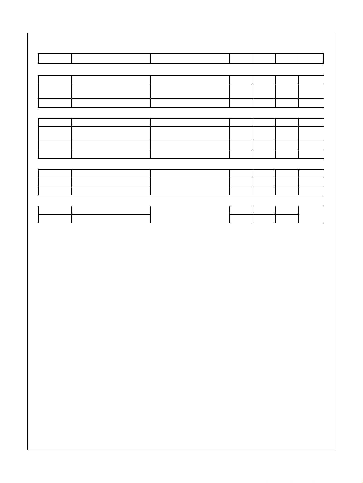
Typical Performance Characteristics
Figure 1. On-Region Characteristics Figure 2. On-Resistance Variation with Gate
Voltage and Drain Current
1.6
1.4
1.2
1.0
0.8
0.6
0.4
. DRAIN-SOURCE CURRENT(A)
D
I
0.2
0.0
012345678910
VGS = 10V
5V
4V
3V
VDS. DRAIN-SOURCE VOLTAGE (V)
2V
3.0
2.5
VGS = 3V
4V
4.5V
(Ω)
(on),
2.0
DS
R
1.5
DRANI-SOURCE ON-RESISTANCE
1.0
0.0 0.2 0.4 0.6 0.8 1.0
7V
ID. DRAIN-SOURCE CURRENT(A)
5V
6V
9V
8V
2N7002DW — N-Channel Enhancement Mode Field Effect Transistor
10V
Figure 3. On-Resistance Variation with
Temperature
3.0
Figure 4. On-Resistance Variation with
Gate-Source Voltage
3.0
VGS = 10V
I
2.5
2.0
(Ω)
(on)
DS
1.5
R
1.0
DRANI-SOURCE ON-RESISTANCE
0.5
-50 0 50 100 150
= 500 mA
D
TJ. JUNCTION TEMPERATURE(oC)
2.5
(Ω)
2.0
(on),
DS
R
DRANI-SOURCE ON-RESISTANCE
ID = 50 mA
1.5
1.0
246810
ID = 500 mA
VGS. GATE-SOURCE VOLTAGE (V)
Figure 5. Transfer Characteristics Figure 6. Gate Threshold Variation with
Temperature
1.0
0.8
0.6
0.4
VDS = 10V
TJ = -25oC
25oC
150oC
125oC
75oC
2.5
2.0
ID = 1 mA
ID = 0.25 mA
1.5
VGS = V
DS
0.2
. DRAIN-SOURCE CURRENT(A)
D
I
0.0
23456
VGS. GATE-SOURCE VOLTAGE (V)
Vth, Gate-Source Threshold Voltage (V)
1.0
-50 0 50 100 150
TJ. JUNCTION TEMPERATURE(oC)
© 2007 Fairchild Semiconductor Corporation www.fairchildsemi.com
2N7002DW Rev. A 3

Typical Performance Characteristics
2N7002DW — N-Channel Enhancement Mode Field Effect Transistor
Figure 7. Reverse Drain Current Variation with
Diode Forward Voltage and Temperature
VGS = 0 V
100
10
Reverse Drain Current, [mA]
S
I
1
0.0 0.2 0.4 0.6 0.8 1.0
VSD, Body Diode Forward Voltage [V]
150oC
25oC
-55oC
Figure 8. Power Derating
280
240
200
160
120
80
40
[mW], POWER DISSIPATION
C
P
0
0 25 50 75 100 125 150 175
Ta[oC], AMBIENT TEMPERATURE
© 2007 Fairchild Semiconductor Corporation www.fairchildsemi.com
2N7002DW Rev. A 4

Package Dimensions
2N7002DW — N-Channel Enhancement Mode Field Effect Transistor
SC70-6 ( SOT-363 )
© 2007 Fairchild Semiconductor Corporation www.fairchildsemi.com
2N7002DW Rev. A 5

TRADEMARKS
The following are registered and unregistered trademarks and service marks Fairchild Semiconductor owns or is authorized to use and
is not intended to be an exhaustive list of all such trademarks.
®
ACEx
Build it Now™
CorePLUS™
CROSSVOLT™
CTL™
Current Transfer Logic™
EcoSPARK
Fairchild
®
®
Fairchild Semiconductor
FACT Quiet Series™
®
FACT
®
FAST
FastvCore™
FPS™
®
FRFET
Global Power Resource
Green FPS™
Green FPS™ e-Series™
GTO™
i-Lo™
IntelliMAX™
ISOPLANAR™
MegaBuck™
MICROCOUPLER™
®
SM
MicroFET™
MicroPak™
Motion-SPM™
OPTOLOGIC
OPTOPLANAR
®
PDP-SPM™
Power220
®
®
®
Power247
POWEREDGE
Power-SPM™
PowerTrench
Programmable Active Droop™
QFET
QS™
QT Optoelectronics™
Quiet Series™
RapidConfigure™
SMART START™
SPM
STEALTH™
SuperFET™
SuperSOT™-3
SuperSOT™-6
®
®
®
®
SuperSOT™-8
SyncFET™
The Power Franchise
TinyBoost™
TinyBuck™
TinyLogic
®
®
TINYOPTO™
TinyPower™
®
TinyPWM™
TinyWire™
µSerDes™
®
UHC
UniFET™
VCX™
2N7002DW N-Channel Enhancement Mode Field Effect Transistor2N7002DW
DISCLAIMER
FAIRCHILD SEMICONDUCTOR RESERVES THE RIGHT TO MAKE CHANGES WITHOUT FURTHER NOTICE TO ANY PRODUCTS
HEREIN TO IMPROVE RELIABILITY, FUNCTION, OR DESIGN. FAIRCHILD DOES NOT ASSUME ANY LIABILITY ARISING OUT OF
THE APPLICATION OR USE OF ANY PRODUCT OR CIRCUIT DESCRIBED HEREIN; NEITHER DOES IT CONVEY AN Y LICENSE
UNDER ITS PATENT RIGHTS, NOR THE RIGHTS OF OTHERS. THESE SPECIFICATIONS DO NOT EXPAND THE TERMS OF
FAIRCHILD’S WORLDWIDE TERMS AND CONDITIONS, SPECIFICALLY THE WARRANTY THEREIN, WHICH COVERS THESE
PRODUCTS.
LIFE SUPPORT POLICY
FAIRCHILD’S PRODUCTS ARE NOT AUTHORIZED FOR USE AS CRITICAL COMPONENTS IN LIFE SUPPORT DEVICES OR
SYSTEMS WITHOUT THE EXPRESS WRITTEN APPROVAL OF FAIRCHILD SEMICONDUCTOR CORPORATION.
As used herein:
1. Life support devices or systems are devices or systems
which, (a) are intended for surgical implant into the body, or
(b) support or sustain life, and (c) whose failure to perform
when properly used in accordance with instructions for use
2. A critical component is any component of a life support
device or system whose failure to perform can be reasonably
expected to cause the failure of the life support device or
system, or to affect its safety or effectiveness.
provided in the labeling, can be reasonably expected to result
in significant injury to the user.
PRODUCT STATUS DEFINITIONS
Definition of Terms
Datasheet Identification Product Status Definition
Advance Information Formative or In Design
This datasheet contains the design specifications for product development.
Specifications may change in any manner without notice.
This datasheet contains preliminary data; supplementary data will be pub-
Preliminary First Production
lished at a later date. Fairchild Semiconductor reserves the right to make
changes at any time without notice to improve design.
No Identification Needed Full Production
This datasheet contains final specifications. Fairchild Semiconductor reserves
the right to make changes at any time without notice to improve design.
This datasheet contains specifications on a product that has been discontin-
Obsolete Not In Production
ued by Fairchild semiconductor. The datasheet is printed for reference information only.
Rev. I30
© 2007 Fairchild Semiconductor Corporation www.fairchildsemi.com
2N7002DW Rev. A 6
 Loading...