Fairchild MMBT3906, PZT3906, 2N3906 Schematics

2N3906 / MMBT3906 / PZT3906
2N3906
MMBT3906
PZT3906
EBC
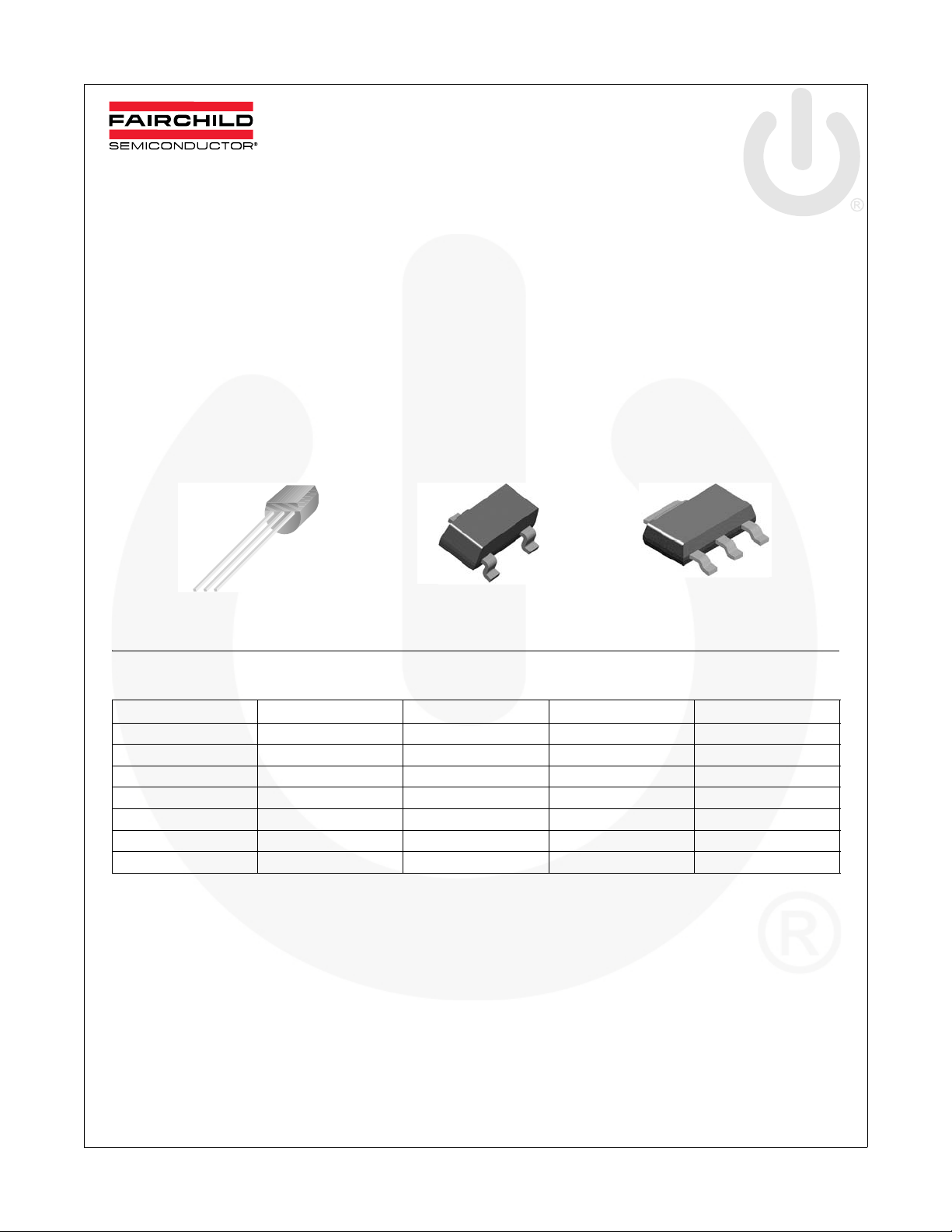
TO-92 SOT-23 SOT-223
Mark:2A
C
B
E
E
B
C
C
PNP General Purpose Amplifier
2N3906 / MMBT3906 / PZT3906 — PNP General Purpose Amplifier
September 2013
Description
This device is designed for general purpose amplifier
and switching applications at collector currents of 10 mA
to 100 mA.
Ordering Information
Part Number Marking Package Packing Method Pack Quantity
2N3906BU 2N3906 TO-92 Bulk 10000
2N3906TA 2N3906 TO-92 Ammo 2000
2N3906TAR 2N3906 TO-92 Ammo 2000
2N3906TF 2N3906 TO-92 Tape and Reel 2000
2N3906TFR 2N3906 TO-92 Tape and Reel 2000
MMBT3906 2A SOT-23 Tape and Reel 3000
PZT3906 3906 SOT-223 Tape and Reel 2500
© 2010 Fairchild Semiconductor Corporation www.fairchildsemi.com
2N3906 / MMBT3906 / PZT3906 Rev. 1.2.1 1

2N3906 / MMBT3906 / PZT3906 — PNP General Purpose Amplifier
Absolute Maximum Ratings
(1)
Stresses exceeding the absolute maximum ratings may damage the device. The device may not function or be operable above the recommended operating conditions and stressing the parts to these levels is not recommended. In addition, extended exposure to stresses above the recommended operating cond itions may affect device reliability. The
absolute maximum ratings are stress ratings only. Values are at T
= 25°C unless otherwise noted.
A
Symbol Parameter Value Units
V
CEO
V
CBO
V
EBO
I
C
T
J, Tstg
Note:
1. These ratings are based on a maximum junction temperature of 150 °C.
These are steady-state limits. Fairchild Semiconductor should be consulted on applications involving pulsed
or low-duty cycle operations.
Collector-Emitter Voltage -40 V
Collector-Base Voltage -40 V
Emitter-Base Voltage -5.0 V
Collector Current - Continuous -200 mA
Operating and Storage Junction Temperature Range -55 to +150 °C
Thermal Characteristics
V a lues are at TA = 25°C unless otherwise noted.
Symbol Parameter
P
D
R
θJC
R
θJA
Total Device Dissipation 625 350 1,000 mW
Derate above 25°C5.02.88.0mW/°C
Thermal Resistance, Junction to Case 83.3 °C/W
Thermal Resistance, Junction to Ambient 200 357 125 °C/W
2N3906 MMBT3906
Notes:
2. Device mounted on FR-4 PCB 1.6 inch X 1.6 inch X 0.06 inch.
3. Device mounted on FR-4 PCB 36 mm X 18 mm X 1.5 mm; mounting pad for the collector lead minimum 6 cm
Max.
(2)
PZT3906
(3)
Units
2
.
© 2010 Fairchild Semiconductor Corporation www.fairchildsemi.com
2N3906 / MMBT3906 / PZT3906 Rev. 1.2.1 2

Electrical Characteristics
V a lues are at TA = 25°C unless otherwise noted.
Symbol
OFF CHARACTERISTICS
V
(BR)CEO
V
(BR)CBO
V
(BR)EBO
I
BL
I
CEX
ON CHARACTERISTICS
h
FE
V
CE(sat)
V
BE(sat)
SMALL SIGNAL CHARACTERISTICS
f
T
C
obo
C
ibo
NF Noise Figure
SWITCHING CHARACTERISTICS
t
d
t
t
s
t
Note:
4. Pulse Test: Pulse Width ≤ 300μs, Duty Cycle ≤ 2.0%.
Collector-Emitter Breakdown
Voltage
Collector-Base Breakdown Voltage IC = -10 μA, IE = 0 -40 V
Emitter-Base Breakdown Voltage IE = -10 μA, IC = 0 -5.0 V
Base Cutoff Current VCE = -30 V, VBE = 3.0 V -50 nA
Collector Cutoff Current VCE = -30 V, VBE = 3.0 V -50 nA
DC Current Gain
Collector-Emitter Saturation Voltage
Base-Emitter Saturation Voltage
Current Gain - Bandwidth Product
Output Capacitance
Input Capacitance
Delay Time
Rise Time 35 ns
r
Storage Time
Fall Time 75 ns
f
Parameter Test Condition Min. Max. Units
(4)
(4)
IC = -1.0 mA, IB = 0 -40 V
IC = -0.1 mA, VCE = -1.0 V 60
I
= -1.0 mA, VCE = -1.0 V 80
C
I
= -10 mA, VCE = -1.0 V 100 300
C
I
= -50 mA, VCE = -1.0 V 60
C
I
= -100 mA, VCE = -1.0V 30
C
IC = -10 mA, IB = -1.0 mA -0.25 V
I
= -50 mA, IB = -5.0 mA -0.4 V
C
I
= -10 mA, IB = -1.0 mA -0.65 -0.85 V
C
I
= -50 mA, IB = -5.0 mA -0.95 V
C
= -10 mA, VCE = -20 V,
I
C
f = 100 MHz
V
CB
f = 100 kHz
V
EB
f = 100 kHz
I
= -100 μA, VCE = -5.0 V,
C
R
S
f = 10 Hz to 15.7 kHz
V
CC
= -10 mA, IB1 = -1.0 mA
I
C
V
CC
I
B1
= -5.0 V, IE = 0,
= -0.5 V, IC = 0,
= 1.0 kΩ,
= -3.0 V, VBE = -0.5 V
= -3.0 V, IC = -10 mA,
= IB2 = -1.0 mA
2N3906 / MMBT3906 / PZT3906 — PNP General Purpose Amplifier
250 MHz
4.5 pF
10.0 pF
4.0 dB
35 ns
225 ns
© 2010 Fairchild Semiconductor Corporation www.fairchildsemi.com
2N3906 / MMBT3906 / PZT3906 Rev. 1.2.1 3

Typical Performance Characteristics
2N3906 / MMBT3906 / PZT3906 — PNP General Purpose Amplifier
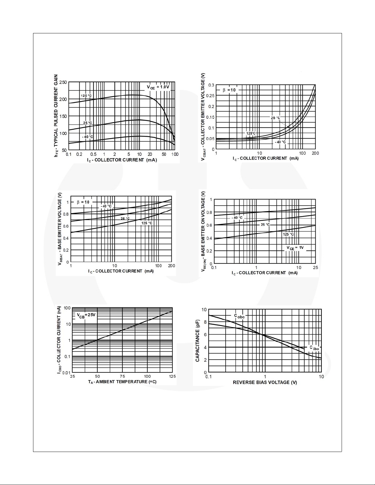
Figure 1. Typical Pulsed Current Gain vs. Collector
Current
Figure 3. Base-Emitter Saturation Voltage
vs. Collector Current
Figure 2. Collector-Emitter Saturation Voltage vs.
Collector Current
Figure 4. Base-Emitter On Voltage vs. Collector
Current
Figure 5. Collector Cut-Off Current vs. Ambient
Temperature
© 2010 Fairchild Semiconductor Corporation www.fairchildsemi.com
2N3906 / MMBT3906 / PZT3906 Rev. 1.2.1 4
Figure 6. Common-Base Open Circuit Input and Out-
put Capacitance vs. Reverse Bias Voltage
 Loading...