

Fairchild 2N3416, 2N3417 service manual
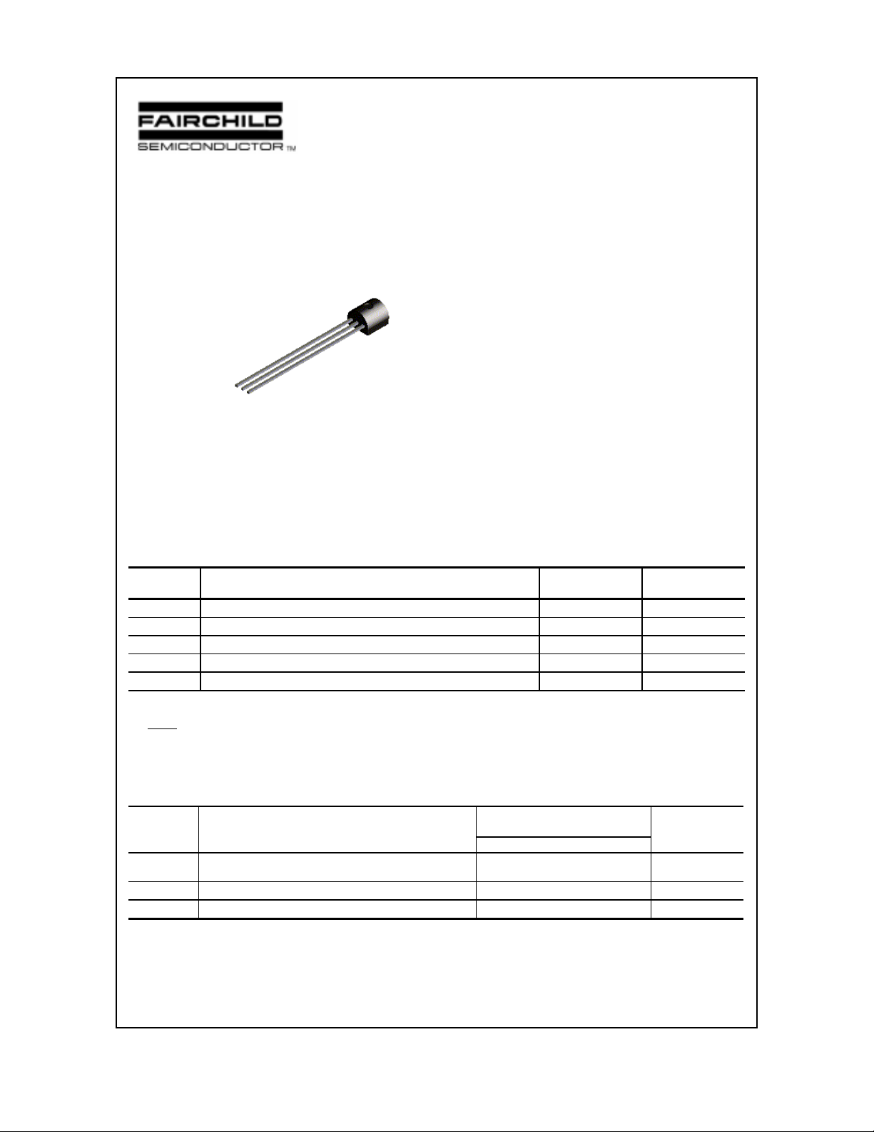
2N3416
2N3417
2N3416 / 2N3417
B
C
E
TO-92
NPN General Purpose Amplifier
This device is designed for use as general purpose amplifiers
and switches requiring collector currents to 300 mA. Sourced
from Process 10. See PN100A for characteristics.
Absolute Maximum Ratings* TA = 25°C unless otherwise noted
Symbol Parameter Value Units
V
CEO
V
CBO
V
EBO
I
C
TJ, T
stg
*These ratings are limiting values above which the serviceability of any semiconductor device may be impaired.
NOTES:
1) These ratings are based on a maximum junction temperature of 150 degrees C.
2) These are steady state limits. The factory should be consulted on applications involving pulsed or low duty cycle operations.
Thermal Characteristics TA = 25°C unless otherwise noted
Collector-Emitter Voltage 50 V
Collector-Base Voltage 50 V
Emitter-Base V ol tage 5.0 V
Collector Current - Continuous 500 mA
Operating and Storage Junction Temperature Range -55 to +150
°C
Symbol Characteristic Max Units
2N3416 / 2N3417
P
D
R
θ
JC
R
θ
JA
1997 Fairchild Semiconductor Corporation
Total Device Dissipation
Derate above 25°C
Thermal Resistance, Junction to Case 83.3
Thermal Resistance, Junction to Ambient 200
625
5.0
mW
mW/°C
°C/W
°C/W
3416-3417, Rev B
NPN General Purpose Amplifier
(continued)
Electrical Characteristics TA = 25°C unless otherwise noted
Symbol Parameter Test Conditions Min Max Units
OFF CHARACTERISTICS
V
(BR)CEO
V
(BR)CBO
V
(BR)EBO
I
CBO
I
EBO
ON CHARACTERISTICS*
h
FE
V
sat
CE(
V
sat
BE(
Collector-Emitter Breakdown
IC = 10 mA, IB = 0 50 V
Voltage*
Collector-Base Breakdown Voltage
Emitter-Base B reakdown Voltage
I
= 10 µA, IE = 0
C
I
= 10 µA, IC = 0
E
50 V
5.0 V
Collector-Cutoff Current VCB = 25 V, IE = 0
= 18 V, IE = 0, TA = 100°C
V
CB
Emitter-Cutoff Current VEB = 5.0 V, IC = 0 100 nA
DC Current Gain VCE = 4.5 V, IC = 2.0 mA
2N3416
2N3417
Collector-Emitter Saturation Voltage IC = 50 mA, IB = 3.0 mA 0.3 V
)
Base-Emitter Saturation Voltage IC = 50 mA, IB = 3.0 mA 0.6 1.3 V
)
75
180
100
15
225
540
nA
µA
2N3416 / 2N3417
SMALL SIGNAL CHARACTERISTICS
h
fe
Small-Signal Current Gain IC = 2.0 mA, VCE = 4.5 V,
*Pulse T est: Pulse Width ≤ 300 µs, Duty Cycle ≤ 2.0%
f = 1.0 kHz 2N3416
2N3417
75
180
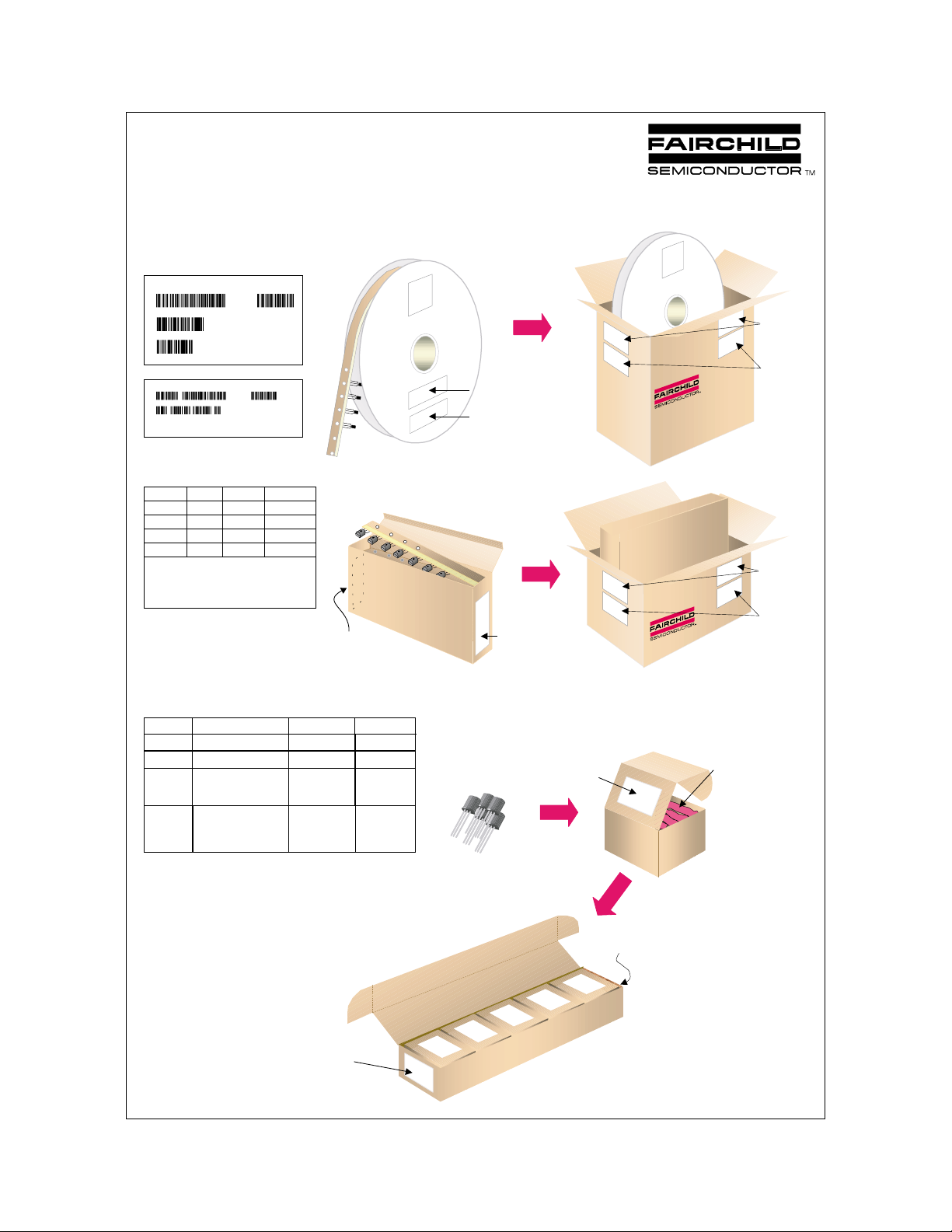
TO-92 Tape and Reel Data
TO-92 Packaging
Configuration: Figure 1.0
FSCINT Label sample
FAIRCHILD SEMICONDUCTOR CORPORATION
LOT:
CBVK741B019
NSID:
PN2222N
D/C1:
SPEC REV:
D9842
QA REV:
HTB:B
QTY:
10000
SPEC:
B2
(FSCINT)
F63TNR Label sample
LOT: CBVK741B019
FSID: PN222N
D/C1: D9842 QTY1: SPEC REV:
D/C2: QTY2: CPN:
QTY: 2000
SPEC:
N/F: F (F63TNR)3
TO-92 TNR/AMMO PACKING INFROMATION
Packing Style Quantity EOL cod e
Reel A 2,000 D26Z
Ammo M 2,000 D74Z
Unit w eight = 0.22 gm
Reel weight with compo nents = 1.0 4 kg
Amm o weig ht with components = 1.02 kg
Max q uantity p er interme d i a te box = 10,0 00 units
E2,000 D27Z
P2,000 D75Z
(TO-92) BULK PACKING INFORMATION
EOL
CODE
J18Z
J05Z
NO EOL
CODE
L34Z
DESCRIPTION
TO-18 OPTION STD NO LEAD CLIP
TO-5 OPTION STD NO LEAD CLIP
TO-92 STANDARD
STRAIGHT FOR: PKG 92,
94 (NON PROELECTRON
SERIES), 96
TO-92 STANDARD
STRAIGHT FOR: PKG 94
(PROELECTRON SERIES
BCXXX, BFXXX, BSRXXX),
97, 98
NO LEADCLIP
NO LEADCLIP
LEADCLIP
DIMENSION
327mm x 158mm x 135mm
Immediate Box
Customized
Label
QUANTITY
2.0 K / BOX
1.5 K / BOX
2.0 K / BOX
2.0 K / BOX
TAPE and REEL OPTION
See Fig 2.0 for various
Reeling Styles
5 Reels per
Intermediate Box
F63TNR
Label
Customized
Label
AMMO PACK OPTION
See Fig 3.0 for 2 Ammo
Pack Options
5 Ammo boxes per
Intermediate Box
F63TNR
Label
BULK OPTION
See Bulk Packing
Information table
FSCINT Label
2000 units per
EO70 box for
std option
375mm x 267mm x 375mm
Intermediate Box
333mm x 231mm x 183mm
Intermediate Box
Anti-static
Bubble Sheets
114mm x 102mm x 51mm
FSCINT
Label
Customized
Label
FSCINT
Label
Customized
Label
Immediate Box
530mm x 130mm x 83mm
FSCINT Label
©2001 Fairchild Semiconductor Corporation
Intermediate box
ustomized
C
Label
10,000 units maximum
per intermediate box
for std option
5 EO70 boxes per
intermediate Box
March 2001, Rev. B1
 Loading...