


EC5-1812CLDNA(B)
5.25〞Single Board Computer
Version: C00

Copyright Notice
Except for the accessories attached to the product as specified herein, what is
contained in this User Manual does not represent the commitments of EVOC
Company. EVOC Company reserves the right to revise this User Manual, without
prior notice, and will not be held liable for any direct, indirect, intended or unintended
losses and/or hidden dangers due to installation or improper operation.
Before purchasin g, please have a detailed understanding of the product performance
to see whether it meets your requirements.
EVOC is a registered trademark of EVOC Intelligent Technology Co., Ltd. All
trademarks, registered trademarks, and trade names used in this User Guide are the
property of their respective owners.
EVOC Intelligent Technology Co., Ltd. ©2008, Copyright Res erved. No part of this
manual may be rep roduced in any form or by an y means, electro nic or mechanical,
without permission in writing from EVOC.
Safety Instructions
1. Before handling your motherboard, read the instructions and safety guidelines
on the following pages to prevent damage to the product and to ensure your own
personal safet y;
2. Any boards or cards not ready to be installed shall be kept in the anti-static
packaging;
3. Before taking board or card from anti-static packaging, put your hand on
grounded metal object for a while (about 10 seconds) to eliminate static on your
body;
4. While fetching a board or card, please wear static protective gloves; hold a
board by its edges or by its metal mounting bracket;
5. Before inserting, removing or re-configuring motherboard or expansion card,
first disconnect the computer and peripherals from their power sources;
6. Before removing boards or computer, first turn off all power resources and
disconnect the power cord from power source;
7. For P C Box products, when inserting or removing boards, first disconnect the
computer and peripherals from their power sources;
8. Before you connect or unplug any equipment, make sure all power cords are
unplugged in advance;
9. To avoid unnecessary damage caused by turning on/off computer frequently,
wait at least 30 seco nds before re-turning on the computer.

Contents
Chapter 1 Produc t I ntroduction ..................................................................................... 1
Overview .................................................................................................................. 1
Environment and Dimensions .................................................................................. 1
Typical Power Consumption .................................................................................... 2
CPU .......................................................................................................................... 2
Chipset ..................................................................................................................... 2
System Memory ....................................................................................................... 2
LAN ......................................................................................................................... 2
IDE Funct ion ............................................................................................................ 2
V ideo Functio n ......................................................................................................... 2
Audio Function ........................................................................................................ 3
I/O Function ............................................................................................................. 3
Expansion Bus ......................................................................................................... 3
Watchdog Function .................................................................................................. 3
Chapter 2 Installation .................................................................................................... 4
Product Outline ........................................................................................................ 4
The Locations of Interfaces ...................................................................................... 5
Jumper Settings ........................................................................................................ 6
SATA Interface ......................................................................................................... 7
Hot-swap of SATA Hard Disk .................................................................................. 7
USB Interface ........................................................................................................... 9
Serial Ports ............................................................................................................. 10

Parallel Port ............................................................................................................ 11
LAN Port ................................................................................................................ 11
Video Interface ....................................................................................................... 12
CF Card .................................................................................................................. 13
PCI Slot .................................................................................................................. 14
PCIE X1 Slots ........................................................................................................ 15
Audio Interface ...................................................................................................... 15
Fan Interface .......................................................................................................... 16
Power Interface ...................................................................................................... 16
Digital I/O Interface ............................................................................................... 16
Status Indicator Interface ....................................................................................... 17
Chapter 3 BIOS Setup ................................................................................................ 18
Appendix .................................................................................................................... 19
Watchdog Programming Guide .............................................................................. 19
GPIO Progra m ming Guide ..................................................................................... 23
I/O Address Map .................................................................................................... 28
IRQ Assignment T able ........................................................................................... 29

Chapter 1 Produc t I ntroduction
EC5-1812CLDNA(B)
- 1 -
Chapter 1 Product Introduction
Overview
EC5-1812CLDNA is an embedded motherboard conforming with 5.25〞single board
structure, with high performance and low cost.
The motherboard supports Intel® Atom™ N230 or Intel® Atom™ N270 CPU with
945GC + ICH7 chipset. It is on board 1GB memory and provides VGA + LVDS
dual display int erface to meet different video requirements. It also provides CF card,
SATA interfaces,abundant I/O ports and PCI expansion interfaces.
The motherboard adopts 5.25 〞 single board structure, which could meet the
requirement of in dustry eager for miniaturization, su ch as face recognition terminal,
advertisement player, off-line IC card intelligent consumption system, portable PC
and so on. The product could be widely used to configure intranet, extranet,
demilitarized zone and network controlling port to meet increased requirement of a
new generation product for bandwidth and reliability.
Environm ent and Dim e nsion s
Operating Environment:
Temperature: 0°C~60°C
Humidity: 5%~90% (Non-condensing);
Storage Tem perature:
Temperature: -20°C~70°C;
Humidity: 5%~95%(Non-condensing);
Dimension: 203. 2 0m m ×146.05mm.

Chapter 1 Product Introduction
- 2 -
EC5-1812CLDNA(B)
Typical Power Consumpt ion
CPU: on board Intel® Atom™ N230/N270 1.6G
Memory: on board 1G Samsung memory IC
+5V@2.17A; +5%/-3%;
+3.3V@0.46A; +5%/-3%;
+12V@0.35A; +5%/-3%;
CPU
Intel® A tom™ N230 1.6GHZ,533MHz FSB BGA437 CPU or Intel® Atom™
Processor N270 (512K Cache,1.60 GHz, 533 MHz FSB) CPU。
Chipset
Intel® 945GC + Intel® ICH7.
System Memory
Support DDRⅡ 533MHz memory, on board 1GB memory
LAN
On board one 10/100/1000Mbps Ethernet controller.
IDE Function
One Compact Flash interface; two SATA interfaces
Video Function
Integrate inside Intel 945GC system; support VGA interface; real ize VGA + LVDS
dual-display via SDVO-LVDS chip; and LVDS supports 24-bit dual-channel screen
design.

Chapter 1 Produc t I ntroduction
EC5-1812CLDNA(B)
- 3 -
Audio Function
Integrate one st andard HDA sound chip on-board, which provides excellent sound
effect.
I/O Function
One high-speed parallel port, support SPP/EPP/ECP standard;
Six USB2.0 interfaces;
Four RS-232 interfaces among which COM1/COM2 could support
RS-422/RS-485 mode;
One 8-lane digital IO Interface (4I/4O).
Expansion Bus
One PCI slot, one PCIE X1 slot. PCI slot could be used independently or to expand 3
PCI devices via P C I transfer card.
Watchdog Function
255 levels, programmable per second;
Overtime interrupt or system reset.

Chapter 2 Installation
- 4 -
EC5-1812CLDNA(B)
Chapter 2 Installation
Product Outline
146.1
203.2
193
5.1
135.9
5.1
(Unit: mm)

Chapter 2 Installation
EC5-1812CLDNA(B)
- 5 -
The Locations of Interfaces
PCI1
PCIE1
AUDIO1
LAN1
FP1
FP3
FP2
JCC1
JCF1
CF1
LPT1
SYSFAN1
PWR1
LVDS2
LVDS1
GPIO1
USB1
USB2
USB3
VGA1
SATA1
SATA2
JLCD1
LCDB1
COM2
COM4
COM1
COM3
JP10
JP9
JP8
JP7
JP6
JP5
JP4
JP3
JP2
JP1

Chapter 2 Installation
- 6 -
EC5-1812CLDNA(B)
Jumper Settings
1. JCC1: Clear/Keep CMOS Settings
CMOS is powered by the button battery on board. Clear CMOS will restore
original settings (factory default). The steps are listed as follows:
(1) Turn off the computer and unplug the power cable;
(2) Instantly short JCC1;
(3) Turn on the computer;
(4) Follow the hint on screen to enter BIOS setup when starting the computer, load
optimized defaults;
(5) Save and exit setu p mode
JCC1
Setup Function
1-2 Open
Normal (Default)
1-2 Short
Clear the content of CMOS, all the BIOS setting
resume to factory default value.
2. CF Card Voltage Selection
JCF1
Setup Function
1-2 Short +3.3V (Default)
2-3 Short +5V
3. LCD Operating V ol t age Selection
JLCD1
Setup Function
1-2 Short +3.3V (Default)
2-3 Short +5V
4. Serial Ports RS232/RS422/RS485 Mode Selection
COM1 and COM2 support RS-232/RS-422/RS-485, optional, among which COM1
selects mode via JP1~JP5 setup, while COM 2 selects mode via JP 6~JP10 setup.
Detailed setup is as follows:

Chapter 2 Installation
EC5-1812CLDNA(B)
- 7 -
JP1/JP6
JP2~JP5/JP7~JP10
Pin Setup
Mode Selection
RS-232 RS-422 RS-485
JP1/JP6 1-2 5-6 3-4
JP2/JP7 1-2 2-3 2-3
JP3/JP8 1-2 2-3 2-3
JP4/JP9 1-2 2-3 2-3
JP5/JP10 1-2 2-3 2-3
SATA Interface
SATA1,SATA2
Pin
Signal Name
1 GND
2 TX+
3 TX4 GND
5 RX6 RX+
7 GND
Hot-swap of SAT A Hard Disk
Notice for hot-swap of SATA hard disk:
(1) The hard disk shall support SATA 2.0 and use 15 pin SATA hard disk power.
(2) The driver of chipset shall support the hot-swap SATA hard disk.
(3) Hot-swap of SATA hard disk with operating system in is forbidden when
system is power-on.

Chapter 2 Installation
- 8 -
EC5-1812CLDNA(B)
Please carry out hot plug as follows, improper operation may destroy the hard disk or
result in data lost.
Hot Plug:
Step1: Please plug the 1 x 4 pin SATA power cable (white) into the power adapter.
Step2: Please co nnect the SATA data cable to the SATA interface of main board.
Step3: Please co nnect the 15-pin SATA power cable (black) to the SATA hard disk.
SATA Data Cable
SATA Power Cable

Chapter 2 Installation
EC5-1812CLDNA(B)
- 9 -
Step4: Please connect th e SATA data cable to th e SATA hard disk.
Hot Unplug
Step1: Uninstall th e hard disk from the device manager.
Step2: Unplug the data cable from the SATA hard disk.
Step3: Unplug the SATA 15-pin power cable (black) from the SATA hard disk.
USB Interface
This motherboard provides USB interfaces in three sets, which could be connected
with 6 standard USB devices.
USB1~USB3
Pin
Signal Name
Pin
Signal Name
1 +5V 2 +5V
3 USB1_Data- 4 USB2_Data5 USB1_Data+ 6 USB2_Data+
7 GND 8 GND
9 NC 10 GND_CHASSIS

Chapter 2 Installation
- 10 -
EC5-1812CLDNA(B)
Serial Ports
The motherboard provides 4 serial ports, all of which are standard 2 x 5-pin box
interfaces and need to be fixed onto the chassis via transfer cable to co nnect with
peripheral equipment. COM1 and COM2 support opti o na l RS-232/RS-422/RS-485,
COM3 and COM4 support RS-232 mode.
COM1/COM2
Pin
Signal Name
RS-232 RS-422 RS-485
1 DCD# TXD- Data2 RXD TXD+ Data+
3 TXD RXD+ X
4 DTR# RXD- X
5 GND GND GND
6 DSR# X X
7 RTS# X X
8 CTS# X X
9 RI# X X
10 NC NC NC
COM3/COM4
Pin
Signal Name
1 DCD#
2 RXD
3 TXD
4 DTR#
5 GND
6 DSR#
7 RTS#
8 CTS#
9 RI#
10 NC

Chapter 2 Installation
EC5-1812CLDNA(B)
- 11 -
Parallel Port
Standard 26-pin parallel port, it could be connected with peripheral equipment
according to your requirement.
LPT1
Pin
Signal Name
Pin
Signal Name
1 STB# 2 AFD#
3 PD0 4 ERR#
5 PD1 6 INIT#
7 PD2 8 SLIN#
9 PD3 10 GND
11 PD4 12 GND
13 PD5 14 GND
15 PD6 16 GND
17 PD7 18 GND
19 ACK# 20 GND
21 BUSY 22 GND
23 PE 24 GND
25 SLCT 26 NC
LAN Port
Provide one on-board 10/100/1000M LAN port. It is a 2×7-pin interface, which
requires transfer cable to fix the interface onto the chassis and then connect with
peripheral equipment. The pin arrangement and its corresponding input socket are
showed as follows:
LAN1
Pin
Signal Name
Pin
Signal Name
1 MX0 2 MX03 MX1+ 4 MX15 MX2+ 6 MX27 MX3+ 8 MX39 GND 10 GND
11 LINK_LED+ 12 LINK_LED13 ACT_LED+ 14 ACT_LED-

Chapter 2 Installation
- 12 -
EC5-1812CLDNA(B)
Video Interface
1. 10-Pin VGA Interface
It requires transfer cable to connect with standard VGA device and its pin
definitions are as follows:
VGA1
Pin
Signal Name
Pin
Signal Name
1 VSYNC 2 HSYNC
3 DDCDATA 4 Red
5 DDCCLK 6 Green
7 +5V 8 Blue
9 GND 10 GND
2. 24-bit Dual-scan LVDS Interface
LVDS1
Pin
Signal Name
Pin
Signal Name
1 LVDSO_D0+ 2 LVDSO_D03 GND 4 GND
5 LVDSO_D1+ 6 LVDSO_D17 GND 8 GND
9 LVDSO_D2+ 10 LVDSO_D211 GND 12 GND
13 LVDSO_CLK+ 14 LVDSO_CLK15 GND 16 GND
17 LVDSO_D3+ 18 LVDSO_D319 VDD 20 VDD
LVDS2
Pin
Signal Name
Pin
Signal Name
1 LVDSE_D0+ 2 LVDSE_D03 GND 4 GND
5 LVDSE_D1+ 6 LVDSE_D17 GND 8 GND
9 LVDSE_D2+ 10 LVDSE_D2-
11 GND 12 GND
13 LVDSE_CLK+ 14 LVDSE_CLK15 GND 16 GND
17 LVDSE_D3+ 18 LVDSE_D319 VDD 20 VDD

Chapter 2 Installation
EC5-1812CLDNA(B)
- 13 -
CF Card
Compact Flash card is a rapid storage, which is small in size and easy to use. Its
storage capacit y varies with different cards, like 128M, 256M, et c. CF card could onl y
be inserted in one direction.
Pin
Signal Name
Pin
Signal Name
1 GND 26 CD1#
2 D3 27 D11
3 D4 28 D12
4 D5 29 D13
5 D6 30 D14
6 D7 31 D15
7 CS0# 32 CS1#
8 GND 33 VS1#
9 ATASEL# 34 IOR#
10 GND 35 IOW#
11 GND 36 WE#
12 GND 37 IRQ
13 VCC 38 VCC
14
GND
39 CSEL#
15
GND
40 VS2#
16
GND
41 RESET#
17
GND
42 IORDY
18 A2 43 DREQ
19 A1 44 DACK#
20 A0 45 DASP#
21 D0 46 ATA66_DET
22 D1 47 D8
23 D2 48 D9
24 WP/IOCS16# 49 D10
25 CD2# 50 GND

Chapter 2 Installation
- 14 -
EC5-1812CLDNA(B)
PCI Slot
Marked as PCI1 in figu res
Pin Signal Name Pin Signal Name Pin Signal Name Pin Signal Name
A1 TRST# A31 PCI_AD18 B1 -12V B31 +3.3V
A2 +12V A32 PCI_AD16 B2 TCK B32 PCI_AD17
A3 TMS A33 +3.3V B3 GND B33 PCI_C/BE#2
A4 TDI A34 PCI_FRAME# B4 TDO B34 GND
A5 +5V A35 GND B5 +5V B35 PCI_IRDY#
A6 INTA# A36 PCI_TRDY# B6 +5V B36 +3.3V
A7 INTC# A37 GND B7 INTB# B37 PCI_DEVSEL#
A8 +5V A38 PCI_STOP# B8 INTD# B38 GND
A9 CLK_PCI2 A39 +3.3V B9 PCI_REQ3# B39 PCI_PLOCK#
A10 +5V A40 SDONE B10 PCI_REQ1# B40 PCI_PERR#
A11 CLK_PCI3 A41 SBO# B11 PCI_GNT3# B41 +3.3V
A12 GND A42 GND B12 GND B42 PCI_SERR#
A13 GND A43 PCI_PAR B13 GND B43 +3.3V
A14 PCI_GNT1# A44 PCI_AD15 B14 CLK_PCI0 B44 PCI_C/BE#1
A15 PCI_RST# A45 +3.3V B15 GND B45 PCI_AD14
A16 +5V A46 PCI_AD13 B16 CLK_PCI1 B46 GND
A17 PCI_GNT0# A47 PCI_AD11 B17 GND B47 PCI_AD12
A18 GND A48 GND B18 PCI_REQ0# B48 PCI_AD10
A19 PCI_REQ2# A49 PCI_AD9 B19 +5V B49 GND
A20 PCI_AD30 A50 PCI_C/BE#0 B20 PCI_AD31 B50 PCI_AD8
A21 +3.3V A51 +3.3V B21 PCI_AD29 B51 PCI_AD7
A22 PCI_AD28 A52 PCI_AD6 B22 GND B52 +3.3V
A23 PCI_AD26 A53 PCI_AD4 B23 PCI_AD27 B53 PCI_AD5
A24 GND A54 GND B24 PCI_AD25 B54 PCI_AD3
A25 PCI_AD24 A55 PCI_AD2 B25 +3.3V B55 GND
A26 PCI_GNT2# A56 PCI_AD0 B26 PCI_C/BE#3 B56 PCI_AD1
A27 +3.3V A57 +5V B27 PCI_AD23 B57 +5V
A28 PCI_AD22 A58 PCI_REQ64# B28 GND B58 PCI_ACK64#
A29 PCI_AD20 A59 +5V B29 PCI_AD21 B59 +5V
A30 GND A60 +5V B30 PCI_AD19 B60 +5V
Chapter 2 Installation
EC5-1812CLDNA(B)
- 15 -
PCIE X1 Slots
Marked as PCIE1 in figures
Pin
Signal Name
Pin
Signal Name
B1 +12V A1 PRSNT1#
B2 +12V A2 +12V
B3 RSVD A3 +12V
B4 GND A4 GND
B5 SMCLK A5 TCK
B6 SMDAT A6 TDI
B7 GND A7 TDO
B8 +3.3V A8 TMS
B9 TRST# A9 +3.3V
B10 +3.3Vaux A10 +3.3V
B11 WAKE# A11 PWRGD
B12 RSVD A12 GND
B13 GND A13 REFCLK+
B14 PETp0 A14 REFCLKB15 PETn0 A15 GND
B16 GND A16 PERp0
B17 PRSNT2# A17 PERn0
B18 GND A18 GND
Audio Interface
AUDIO1
Pin
Signal Name
Pin
Signal Name
1 LOUT_R 2 LOUT_L
3 GND_AUDIO 4 GND_AUDIO
5 LIN_R 6 LIN_L
7 GND_AUDIO 8 GND_AUDIO
9 MIC_L 10 MIC_R

Chapter 2 Installation
- 16 -
EC5-1812CLDNA(B)
Fan Interface
The current for fan shall not exceed 350 mA (4.2W, 12V);
P lease confirm that th e fan cable complies with t he socket cable. Power cable
(usually red) is in the middle position. In addition, please pay attention to the
earth cable (usually black) and fan rev output impulse signal cable (other
colors). It is recommended to use a fan with rev speed d etection.
Adjust the fan’s airflow to the direction of heat venting.
SYSFAN1
Pin
Signal Name
1 GND
2 +12V
3 FAN_IO
4 FAN_PWM
FAN_IO: fan rev impulse output; FAN_PWM: fan rev PWM control
Power Interface
10-PIN ATX power interface
PWR1
Pin
Signal Name
Pin
Signal Name
1 PS_ON# 6 +5VSB
2 GND 7 +5V
3 GND 8 +5V
4 +12V 9 -12V
5 +3.3V 10 GND
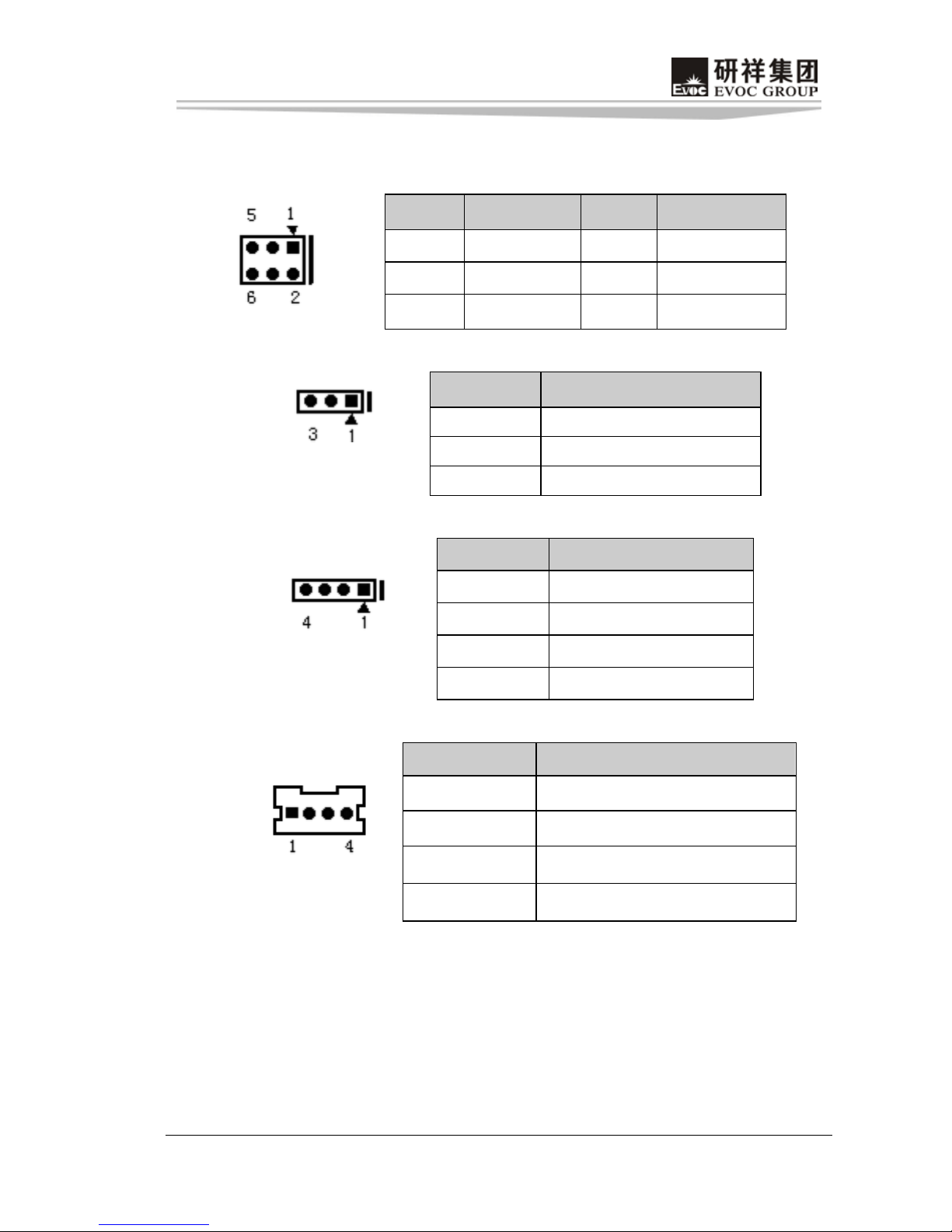
Digital I/O Interface
Provide with 4-lane I/O GPIO interface.
GPIO1
Pin
Signal Name
Pin
Signal Name
1 INPUT1 2 OUTPUT1
3 INPUT2 4 OUTPUT2
5 INPUT3 6 OUTPUT3
7 INPUT4 8 OUTPUT4
9 GND 10 NC

Chapter 2 Installation
EC5-1812CLDNA(B)
- 17 -
Status Indicator Interface
(1) Power Switch and HD Indicator Interfac e
FP1
Pin
Signal Name
Pin
Signal Name
1 PWRBTN# 2 GND
3 GND 4 RESET#
5 IDE_LED- 6 IDE_LED+
(2) Power Indicator Int erface
FP2
Pin
Signal Name
1 PWR_LED+
2 NC
3 GND
(3) Loudspeaker Indicator Interface
FP3
Pin
Signal Name
1 SPEAKER
2 NC
3 GND
4 +5V
(4) LCD Backlight Control Connector
LCDB1
管脚 信号名称
1 VCC_LCDBKLT
2 NC
3 LCD_BKLTEN
4 GND
Note: VCC_LCDBKLT---backlight power (Provides +12V voltage and t he
current o f the pi n is limited below 1A);
LCD_BKLTEN ---backlight enable, active high.

Chapter 3 BIOS Setup
- 18 -
EC5-1812CLDNA(B)
Chapter 3 BIOS Setup
Regarding the BIOS features setup of EC5-1812CLDNA, please refer to the AMI
BIOS Setup Guide edited by EVOC Company.

Appendix
EC5-1812CLDNA(B)
- 19 -
Appendix
Watchdog Programming Guide
EC5-1812CLDNA provides a programmable watchdog timer (WDT) up to 255 levels
and time by minute or second. Watchdog timer overtime event can be programmed to
reset system or generate shielding interrupts.
The following describes WDT program in C language. Note: before operating WDT,
users shall firstly enter WDT programming mode; after finishing WDT configuration,
exit WDT.
The steps to program WDT:
Enter WDT programming mode
Setup WDT operatin g methods/ enable WDT/disable WDT
Exit WDT programming mode
The following files shall be included:
#include <stdio.h>
#include <dos.h>
#include <bios.h>
#include <stdlib.h>
#include <string.h>
(1) Enter WDT programming Mode and o btain pm BASE. The watchdog setup
is within pm_base + offset register.
outportb(0x2e,0x55); //enter WDT programming mode, write 0x55 in INDEX PORT
//INDEX PORT [4e /2e], DATA PORT [4F/2F]
// read-in register in INDEX, write-in data to register
from DATA.
outportb(0x2e,0x07); //reg0X07, used to select logic device
outportb(0x2f,0x0A); //select logic deviceA,

Appendix
- 20 -
EC5-1812CLDNA(B)
outportb(0x2e,0x30); //reg0x30, device enables the register, 0=disable, 1=enable
outportb(0x2f,0x01); //enable deviceA
unsigned int ba s e _a ddr;
outportb(0x2e,0x60); //reg60,get high base from this register
base_addr=inportb(0x2f); //and save to global V AR pm_Base
pm_base=base_addr;
outportb(0x2e,0x61); //reg61,get low base from this register
base_addr=inportb(0x2f); //and save to global V AR pm_Base
pm_base=pm_base<<8;
pm_base=pm_base+base_addr;
#define WRITEREG(reg,val) {tmp_reg=pm_base+reg; outportb(tmp_reg,val);}
(2) Setup WDT operating mo de, reset mode or interrupt mode:
a. Reset Operating Mode
WRITEREG(0x47,0x0c)
/* pm_base+offset 0x47
register 0 x47
bit[0]in/out: 1=input,0=output
bit[1]polarity:1=invert ,0=no invert
bit[3:2] Alternate Function Select
11=WDT
10=Either Edge Triggered Interrupt Input

Appendix
EC5-1812CLDNA(B)
- 21 -
01=LED1
00=GPIO
bit[6:4] R es er ved
bit[7] Output Type Select
1=Open Drai n
0=Push Pull
*/
b. Interrupt Operating Mode
irq=irq<<4;
WRITEREG(0x47,0x80) // pm_base+offset 0x47
WRITEREG(0x67,irq) // pm_base+offset 0x47
/*
register 0x67
bit[7:4]WD T interrupt Mapp i ng
1111=IRQ 15
.......
0011=IRQ3
0010=IRQ2
0001=IRQ1
0000=Disable
*/
Among which, IRQ_RESOURCE =0: any interrupt is forbidden
(3) WDT timer selection: min ute or second
a. Select to time by minute with the f o llowing words :
;suppose it is under WDT programming mode
WRITEREG(0x65,0)

Appendix
- 22 -
EC5-1812CLDNA(B)
/*
pm_base+offset 0x65
register 0x65,Watch Dog timeout
bit[7]WDT timeout value Unit Select
0=MInutes(default)
1=Seconds
*/
b. Select to time by second with the fol lowing words:
;suppose it is under WDT programming mode
WRITEREG(0x65,0x80)
(4) Enable/Disable WDT
;suppose it is under WDT programming mode
WRITEREG(0x66, TIME-OUT-VALUE) ;// pm_base+offset 0x66
//write-in preset time
TIME-OUT-VALUE
Note: the ran ge of TIME-OUT-VALUE is from 1 to 255, the unit is “second” or
“minute”. If TIME-OUT-VALUE is zero, WDT is disabled.
Start WDT when TIME-OUT-VALUE is non-zero value only.
(5) Exit WDT Programming Mode
Outportb (0x2e, 0x00);

Appendix
EC5-1812CLDNA(B)
- 23 -
GPIO Programming Guide
The motherboard provides a 4-bit digital I/O port. The following describes digital I/O
ports programming in C language. Note: before operating the digital I/O port, please
enter digital I/O ports programming mode first; after completing this operation, please
exit digital I/O ports programming mode.
The programming steps are as follows:
Enter digital I/O ports programming mode
Implement input/output operation fo r d igital I/O port
Exit digital I/O ports programming mode
Please refer to the following code for digital I/O port p ro gramming:
unsigned long _pascal in_32(unsigned int io_port)
{
unsigned long ReturnValue;
_asm{
mov dx,io_port
in eax,dx
mov ReturnValue,eax
}
return ReturnValue;
}
void _pascal out_32(unsigned int io_port, unsigned long io_data)
{
_asm{
mov dx, io_port
mov eax, io_data
out dx, eax

Appendix
- 24 -
EC5-1812CLDNA(B)
}
}
long read_pci(long addr)
{
long pci_data;
out_32( 0xCF8, addr );
pci_data = in_32( 0xCFC );
return(pci_data);
}
long Write_pci(long addr, long data)
{
long pci_data;
out_32( 0xCF8, addr );
out_32( 0xcfc, data );
return(pci_data);
}
long addr_pci= 0x8000F848;
long io_base=read_pci(addr_pci) & 0x0000fffe //Bus:0 Dev:1F Fun:0
Reg:48(Dword Reg) get Base
Address
unsigned int addr_statue=io_base+0x1a;
outportb(addr_statue,0x00);
addr_statue=io_base+0x1b;
outportb(addr_statue,0x00); //base +offset 1ah /1bh GPIO Blink

Appendix
EC5-1812CLDNA(B)
- 25 -
Register Don’t BLINK
//select as GPIO
unsigned int addr_select=io_base+0x02;
unsigned int ge t _ 1x = i np or t b(addr_select)| 0x 05;
outportb(addr_select,get_1x); //base+offset2h GPIO Use
Select Register
bit[0]=1,
bit[2]=1 ;selset
GP16,GP18 as GPIO
addr_select=io_base+0x03;
unsigned int ge t _ 2x = i np or t b(addr_select)| 0x 1c;
outportb(addr_select,get_2x); //base+offset3h GPIO Use
Select Register
bit[4:2]=111;selset
GP28~GP26 as
GPIO ,
addr_select=io_base+0x30;
unsigned int ge t _ 3x = i np or t b(addr_select)| 0xc 2;
outportb(addr_select,get_3x); //base+offset30h GPIO Use

Appendix
- 26 -
EC5-1812CLDNA(B)
Select Register
bit[1]=1,bit[7:6]=
11;selset
GP33,GP38,GP3
9as GPIO
//select as INPUT or OUTPUT
unsigned int addr_select2=io_base+0x06;
unsigned int ge t _ 0= i n por t b( a ddr_select2)|0x04;
get_0=get_0&0xfe ;
outportb(addr_select2,get_0); //base+offset6h GPIO IN/OUT
Select Register
bit[0]=0,bit[2]=1,;selset
GP18 as input ,GP16 as
output ;
addr_select2=io_base+0x07;
unsigned int ge t _ 2= i n por t b( a ddr_select2)&0x e 3;
outportb(addr_select2,get_2); //base+offset7h GPIO
IN/OUT Select Register
bit[4:2]=000; selset
GP28~GP26 as output
addr_select2=io_base+0x34;
unsigned int ge t _ 3= i n por t b( a ddr_select2)|0xc 2;
outportb(addr_select2,get_3); //base+offset34h GPIO Use

Appendix
EC5-1812CLDNA(B)
- 27 -
Select Register
bit[1]=1,bit[7:6]=
11;selset
GP33,GP38,GP3
9as input
// OUTPUT 0 or 1
unsigned int addr_o1=io_base+0x0e;
unsigned int addr_o2=io_base+0x0f; // get output base
unsigned int addr_i1=io_base+0x0e;
unsigned int addr_i3=io_base+0x38; //get input base
unsigned int num_1=inportb(addr_o1)&0xfe;
outportb(addr_o1,num_1);
unsigned int num_2=inportb(addr_o2)&0xe3;
outportb(addr_o2,num_2);
Set the output pin as low level, short circuit I/O pins and then measure the voltage on
input pin. If the voltage value on the input pin is low, then IO digtial is normal;
otherwise, it is abnormal. Users may also set the output pin as high level by the same
way. Short circuit and test on the output pin to see whether it is on high level.

Appendix
- 28 -
EC5-1812CLDNA(B)
I/O Address Map
There is 64K for the system I/O address space. Each external device will occupy
portion of the space. The table below shows parts of the distribution of the I/O
address. As the address of PCI device (e.g. PCI network card) is configured by
software, it is not listed in this table.
Address Device description
000h-00Fh DMA Controller
020h–021h Interrupt Controller
040h–043h Timer
061h System Loudspeaker
070h-071h Real Time Clock
081h-083h DMA Controller
087h DMA Controller
089h-08Bh DMA Controller
08Fh DMA Controller
0A0h-0A1h Interrupt Controller
0C0h-0DFh DMA Controller
0F0h-0FFh Data Processor
170h-177h Slave IDE
1F0h-1F7h Master IDE
200h-207h Communica t ion P ort (COM3)
208h-20Fh Communication Port (COM4)
274h–277h ISAPNP Data Reading Port
279h ISAPNP Data Reading Port
2F8h–2FFh Communicat ion P ort (COM2)
376h Slave IDE
378h–37Fh Printer Port (LPT1)
3B0h–3DFh Intel 945 Chipset
3F6h Master IDE
3F8h-3FFh Communica t ion P ort (COM1)
400h–41Fh South Bridge Controller

Appendix
EC5-1812CLDNA(B)
- 29 -
IRQ Assignment T able
There are 11 interrupt sources in the EC 5-1812CLDNA serial interrupt controllers and
APIC interrupt controllers, which are compatible with ISA interrupt controllers. Some
are occupied by the system device. Only the ones which are not occupied can be
distributed. The ISA devices claim to engross the interrupt. Only the plug and play
ISA devices can be distributed by the BIOS or the OS. PCI devices use APIC interrupt
and are distributed by OS. The diagram below shows the interrupt distribution
compatible with ISA:
Level Function
IRQ0 System Timer
IRQ3 Serial Port #3, #4
IRQ4 Serial Port #1, #2
IRQ8 System CMOS/Real Time Clock
IRQ9 ACPI A daptation Sy s tem
IRQ13
Numeric Data Processor
IRQ14
Master IDE
IRQ15
Slave IDE
For more information, pleas e visit our website: http://www.evoc.com

声明
本手册包含的内容并不代表本公司的承诺,本公司保留对此手册更改的权
利,且不另行通知。对于任何因安装、使用不当而导致的直接、间接、有意或无
意的损坏及隐患概不负责。
订购产品前,请向经销商详细了解产品性能是否符合您的需求。
EVOC是研祥智能科技股份有限公司的注册商标。本手册所涉及到的其他商
标,其所有权为相应的产品厂家所拥有。
研祥智能科技股份有限公司©2008,版权所有,违者必究。未经许可,不得
以机械、电子或其它任何方式进行复制。
安全使用小常识
1. 产品使用前,务必仔细阅读产品说明书;
2. 对未准备安装的板卡,应将其保存在防静电保护袋中;
3. 在从防静电保护袋中拿出板卡前,应将手先置于接地金属物体上一会儿(比
如 10 秒钟),以释放身体及手中的静电;
4. 在拿板卡时,需佩戴静电保护手套,并且应该养成只触及其边缘部分的习
惯;
5. 为避免人体被电击或产品被损坏,在每次对主板、板卡进行拔插或重新配
置时,须先关闭交流电源或将交流电源线从电源插座中拔掉;
6. 在需对板卡或整机进行搬动前,务必先将交流电源线从电源插座中拔掉;
7. 对整机产品,需增加/减少板卡时,务必先拔掉交流电源;
8. 当您需连接或拔除任何设备前,须确定所有的电源线事先已被拔掉;
9. 为避免频繁开关机对产品造成不必要的损伤,关机后,应至少等待 30 秒后
再开机。

目 录
第一章 产品介绍 ...................................................................................................... 1
简介 ......................................................................................................................... 1
环境与机械尺寸 ...................................................................................................... 1
典型功耗 ................................................................................................................. 2
微处理器 ................................................................................................................. 2
芯片组 ..................................................................................................................... 2
系统存储器 .............................................................................................................. 2
网络功能 ................................................................................................................. 2
IDE 功能 ................................................................................................................. 2
显示功能 ................................................................................................................. 3
音频功能 ................................................................................................................. 3
I/O 功能 .................................................................................................................. 3
扩展总线 ................................................................................................................. 3
Watchdog 功能 ....................................................................................................... 3
第二章 安装说明 ...................................................................................................... 4
产品外形尺寸图 ...................................................................................................... 4
接口位置示意图 ...................................................................................................... 5
跳线功能设置 .......................................................................................................... 6
SATA接口 ................................................................................................................. 7
SATA硬盘热插拔 ...................................................................................................... 7
USB接口 ................................................................................................................... 9
串口 ....................................................................................................................... 10

并口 ....................................................................................................................... 11
网络接口 ............................................................................................................... 11
显示接口 ............................................................................................................... 12
CF卡 ....................................................................................................................... 13
PCI插槽 ................................................................................................................. 14
PCIE X1 插槽 ......................................................................................................... 15
音频接口 ............................................................................................................... 15
风扇接口 ............................................................................................................... 16
电源接口 ............................................................................................................... 16
数字I/O接口 ......................................................................................................... 16
状态指示控制接口 ................................................................................................ 17
第三章 BIOS功能简介 ........................................................................................... 18
附录 ............................................................................................................................ 19
Watchdog编程指引 ................................................................................................ 19
数字IO端口编程指引 ............................................................................................ 23
I/O口地址映射表 .................................................................................................. 28
IRQ中断分配表 ...................................................................................................... 29

第一章 产品介绍
EC5-1812CLDNA(B) - 1 -
第一章 产品介绍
简介
EC5-1812CLDNA是一款高性能、低成本的、遵从5.25寸单板结构的嵌入式主
板。
该主板采用Intel® Atom™ N230 CPU或Intel® Atom™ N270 CPU,搭配945GC
+ ICH7的芯片组。板载1GB内存,提供VGA + LVDS接口双显示满足不同的显示需
求。同时提供CF卡和SATA接口,丰富的I/O 接口,以及PCI扩展。
该款主板采用5.25寸单板结构,可以满足大多对小型化要求比较强烈的行
业。如:人脸识别终端、广告播放机、离线式IC卡智能刷卡消费系统、便携式计
算机等移动设备。本产品可广泛用于配置内部网、外部网、停火区、配置网络控
制口,满足新一代网络产品对带宽和可靠性的高要求。
环境与机械尺寸
工作环境:
温度:0°C~60°C
湿度:5%~90%(非凝结状态)
贮存环境:
温度:-20°C~70°C
湿度:5%~95%(非凝结状态)
尺寸:203.20mm ×146.05mm

第一章 产品介绍
- 2 - EC5-1812CLDNA(B)
典型功耗
CPU: 板载 Intel® Atom™ N230/N270 1.6G
内存:板载 1G Samsung内存颗粒
+5V@2.17A;+5%/-3%;
+3.3V@0.46A;+5%/-3%;
+12V@0.35A;+5%/-3%;
微处理器
Intel® Atom™ N230 1.6GHZ,533MHz FSB BGA437 CPU或Intel® Atom™
Processor N270 (512K Cache,1.60 GHz, 533 MHz FSB)CPU。
芯片组
Intel® 945GC + Intel® ICH7。
系统存储器
支持DDRⅡ 533MHz内存,板载1GB内存。
网络功能
在板1个10/100/1000Mbps以太网控制器。
IDE 功能
1个Compact Flash接口;2个SATA接口。

第一章 产品介绍
EC5-1812CLDNA(B) - 3 -
显示功能
系统Intel 945GC内集成,支持VGA接口,并通过SDVO转LVDS芯片实现VGA +
LVDS双显示,LVDS支持24位双通道屏设计。
音频功能
板上集成1个标准的HDA音效芯片,提供优质的声音效果。
I/O 功能
1个高速并行接口,支持SPP/EPP/ECP 标准;
6个USB2.0接口;
4个RS-232 接口,其中COM1/COM2可支持RS-422/RS-485模式;
1个八路数字IO接口(4I/4O)。
扩展总线
1个PCI插槽,1个PCIE X1插槽。PCI槽可单独使用也可通过PCI转接卡扩展3
个PCI设备。
Watchdog 功能
255级,可编程按秒;
超时中断或系统复位。

第二章 安装说明
- 4 - EC5-1812CLDNA(B)
第二章 安装说明
产品外形尺寸图
146.1
203.2
1935.1
135.9
5.1
(单位:mm)

第二章 安装说明
EC5-1812CLDNA(B) - 5 -
接口位置示意图
PCI1
PCIE1
AUDIO1
LAN1
FP1
FP3
FP2
JCC1
JCF1
CF1
LPT1
SYSFAN1
PWR1
LVDS2
LVDS1
GPIO1
USB1
USB2
USB3
VGA1
SATA1
SATA2
JLCD1
LCDB1
COM2
COM4
COM1
COM3
JP10
JP9
JP8
JP7
JP6
JP5
JP4
JP3
JP2
JP1

第二章 安装说明
- 6 - EC5-1812CLDNA(B)
跳线功能设置
1. JCC1:CMOS内容清除/保持设置
CMOS由板上钮扣电池供电。清CMOS会导致永久性消除以前系统配置并将其
设为原始(工厂设置)系统设置。其步骤:(1)关闭计算机,断开电源;(2)瞬间
短接JCC1插针;(3)开计算机;(4)启动时按屏幕提示进入BIOS设置,重载最优缺
省值;(5)保存并退出设置。
JCC1
设置
功能
1-2 开路 正常工作状态(Default)
1-2 短路 清除 CMOS 内容,所有 BIOS 设置恢复成出厂值。
2. CF卡电压选择
JCF1
设置
功能
1-2 短路 +3.3V(Default)
2-3 短路 +5V
3. LCD工作电压选择
JLCD1
设 置
功 能
1-2 短路 +3.3V(Default)
2-3 短路 +5V
4. 串口RS232/RS422/RS485模式选择
COM1和COM2支持RS-232/RS-422/RS-485可选,其中COM1通过设置JP1~JP5
实现模式选择,COM2通过设置JP6~JP10来实现模式选择,具体设置如下:

第二章 安装说明
EC5-1812CLDNA(B) - 7 -
JP1(JP6)
JP2~JP5(JP7~JP10)
管脚设置
模式选择
RS-232
RS-422
RS-485
JP1/JP6 1-2 5-6 3-4
JP2/JP7 1-2 2-3 2-3
JP3/JP8 1-2 2-3 2-3
JP4/JP9 1-2 2-3 2-3
JP5/JP10 1-2 2-3 2-3
SATA 接口
SATA1,SATA2
管脚
信号名称
1 GND
2 TX+
3 TX-
4 GND
5 RX-
6 RX+
7 GND
SATA 硬盘热插拔
SATA 硬盘热插拔需注意:
(1) 硬盘必须支持:SATA 2.0 接口,并且采用 15 芯 SATA 硬盘电源接口。
(2) 芯片组驱动程序支持 SATA 硬盘的热插拔。
(3) 不能对操作系统所在的 SATA 硬盘进行带电热插拔。

第二章 安装说明
- 8 - EC5-1812CLDNA(B)
请按照如下步骤进行 SATA 硬盘热插拔,否则,操作不当会导致硬盘损坏和
数据丢失。
热插入SATA硬盘步骤:
步骤1:请将SATA电源线1x4-针脚(白色)一端接到电源适配器的1x4-针脚电
源线一端。
步骤2:将SATA 数据线接到主板上的SATA接口。
步骤3:将SATA电源线15-针脚接口(黑色)一端接到SATA硬盘。
SATA 硬盘数据线 SATA 硬盘电源线

第二章 安装说明
EC5-1812CLDNA(B) - 9 -
步骤4:将SATA数据线接到SATA硬盘。
热拔出SATA硬盘步骤:
步骤 1:从设备管理器中卸载该硬盘。
步骤 2:从 SATA 硬盘一侧拔去 SATA 数据线。
步骤 3:从 SATA 硬盘一侧拔去 SATA 15-针脚电源线接口(黑色)。
USB 接口
本主板提供3组USB接口,可连接6个标准的USB设备。
USB1~USB3
管脚
信号名称
管脚
信号名称
1 +5V 2 +5V
3 USB1_Data- 4 USB2_Data-
5 USB1_Data+ 6 USB2_Data+
7 GND 8 GND
9 NC 10 GND_CHASSIS

第二章 安装说明
- 10 - EC5-1812CLDNA(B)
串口
本主板提供4个串行通讯口,都是标准的2×5针盒式接口,需要用转换电缆
固定到机箱上才能与外部设备连接。其中COM1和COM2支持RS-232/RS-422/RS-485
可选。COM3和COM4支持RS-232模式。
COM1/COM2
管脚
信号名称
RS-232
RS-422
RS-485
1 DCD# TXD- Data-
2 RXD TXD+ Data+
3 TXD RXD+ X
4 DTR# RXD- X
5 GND GND GND
6 DSR# X X
7 RTS# X X
8 CTS# X X
9 RI# X X
10 NC NC NC
COM3/COM4
管脚
信号名称
1 DCD#
2 RXD
3 TXD
4 DTR#
5 GND
6 DSR#
7 RTS#
8 CTS#
9 RI#
10 NC

第二章 安装说明
EC5-1812CLDNA(B) - 11 -
并口
标准的26针并行接口,可依据您的需求用来连接并行接口外设。
LPT1
管脚
信号名称
管脚
信号名称
1 STB# 2 AFD#
3 PD0 4 ERR#
5 PD1 6 INIT#
7 PD2 8 SLIN#
9 PD3 10 GND
11 PD4 12 GND
13 PD5 14 GND
15 PD6 16 GND
17 PD7 18 GND
19 ACK# 20 GND
21 BUSY 22 GND
23 PE 24 GND
25 SLCT 26 NC
网络接口
本主板提供1个在板10/100/1000M LAN接口,是2×7针接口,需要用转接线
固定到机箱上与外部设备连接。以下给出了它的管脚安排和相应的输入插座。
LAN1
管脚
信号名称
管脚
信号名称
1 MX0 2 MX0-
3 MX1+ 4 MX1-
5 MX2+ 6 MX2-
7 MX3+ 8 MX3-
9 GND 10 GND
11 LINK_LED+ 12 LINK_LED-
13 ACT_LED+ 14 ACT_LED-

第二章 安装说明
- 12 - EC5-1812CLDNA(B)
显示接口
1. 10Pin插针VGA接口
需要用转接线接标准VGA设备,其接口定义如下:
VGA1
管脚
信号名称
管脚
信号名称
1 VSYNC 2 HSYNC
3 DDCDATA 4 Red
5 DDCCLK 6 Green
7 +5V 8 Blue
9 GND 10 GND
2. 24bit双扫描LVDS接口
LVDS1
管脚
信号名称
管脚
信号名称
1 LVDSO_D0+ 2 LVDSO_D03 GND 4 GND
5 LVDSO_D1+ 6 LVDSO_D17 GND 8 GND
9 LVDSO_D2+ 10 LVDSO_D211 GND 12 GND
13 LVDSO_CLK+ 14 LVDSO_CLK15 GND 16 GND
17
LVDSO_D3+ 18 LVDSO_D3-
19 VDD 20 VDD
LVDS2
管脚
信号名称
管脚
信号名称
1 LVDSE_D0+ 2 LVDSE_D0-
3 GND 4 GND
5 LVDSE_D1+ 6 LVDSE_D1-
7 GND 8 GND
9 LVDSE_D2+ 10 LVDSE_D211 GND 12 GND
13 LVDSE_CLK+ 14 LVDSE_CLK15 GND 16 GND
17 LVDSE_D3+ 18 LVDSE_D319 VDD 20 VDD
第二章 安装说明
EC5-1812CLDNA(B) - 13 -
CF 卡
Compact Flash卡是一种快速存储器,体积很小,使用方便,存储量随使用
的卡变化,如128M, 256M等。CF卡插入时只能以一个方向插入。
管脚
信号名称
管脚
信号名称
1 GND 26 CD1#
2 D3 27 D11
3 D4 28 D12
4 D5 29 D13
5 D6 30 D14
6 D7 31 D15
7 CS0# 32 CS1#
8 GND 33 VS1#
9 ATASEL# 34 IOR#
10 GND 35 IOW#
11 GND 36 WE#
12 GND 37 IRQ
13 VCC 38 VCC
14
GND
39 CSEL#
15
GND
40 VS2#
16
GND
41 RESET#
17
GND
42 IORDY
18 A2 43 DREQ
19 A1 44 DACK#
20 A0 45 DASP#
21 D0 46 ATA66_DET
22 D1 47 D8
23 D2 48 D9
24 WP/IOCS16# 49 D10
25 CD2# 50 GND

第二章 安装说明
- 14 - EC5-1812CLDNA(B)
PCI 插槽
图示标识为PCI1。
管脚
信号名称
管脚
信号名称
管脚
信号名称
管脚
信号名称
A1 TRST# A31 PCI_AD18 B1 -12V B31 +3.3V
A2 +12V A32 PCI_AD16 B2 TCK B32 PCI_AD17
A3 TMS A33 +3.3V B3 GND B33 PCI_C/BE#2
A4 TDI A34 PCI_FRAME# B4 TDO B34 GND
A5 +5V A35 GND B5 +5V B35 PCI_IRDY#
A6 INTA# A36 PCI_TRDY# B6 +5V B36 +3.3V
A7 INTC# A37 GND B7 INTB# B37 PCI_DEVSEL#
A8 +5V A38 PCI_STOP# B8 INTD# B38 GND
A9 CLK_PCI2 A39 +3.3V B9 PCI_REQ3# B39 PCI_PLOCK#
A10 +5V A40 SDONE B10 PCI_REQ1# B40 PCI_PERR#
A11 CLK_PCI3 A41 SBO# B11 PCI_GNT3# B41 +3.3V
A12 GND A42 GND B12 GND B42 PCI_SERR#
A13 GND A43 PCI_PAR B13 GND B43 +3.3V
A14 PCI_GNT1# A44 PCI_AD15 B14 CLK_PCI0 B44 PCI_C/BE#1
A15 PCI_RST# A45 +3.3V B15 GND B45 PCI_AD14
A16 +5V A46 PCI_AD13 B16 CLK_PCI1 B46 GND
A17 PCI_GNT0# A47 PCI_AD11 B17 GND B47 PCI_AD12
A18 GND A48 GND B18 PCI_REQ0# B48 PCI_AD10
A19 PCI_REQ2# A49 PCI_AD9 B19 +5V B49 GND
A20 PCI_AD30 A50 PCI_C/BE#0 B20 PCI_AD31 B50 PCI_AD8
A21 +3.3V A51 +3.3V B21 PCI_AD29 B51 PCI_AD7
A22 PCI_AD28 A52 PCI_AD6 B22 GND B52 +3.3V
A23 PCI_AD26 A53 PCI_AD4 B23 PCI_AD27 B53 PCI_AD5
A24 GND A54 GND B24 PCI_AD25 B54 PCI_AD3
A25 PCI_AD24 A55 PCI_AD2 B25 +3.3V B55 GND
A26 PCI_GNT2# A56 PCI_AD0 B26 PCI_C/BE#3 B56 PCI_AD1
A27 +3.3V A57 +5V B27 PCI_AD23 B57 +5V
A28 PCI_AD22 A58 PCI_REQ64# B28 GND B58 PCI_ACK64#
A29 PCI_AD20 A59 +5V B29 PCI_AD21 B59 +5V
A30 GND A60 +5V B30 PCI_AD19 B60 +5V
第二章 安装说明
EC5-1812CLDNA(B) - 15 -
PCIE X1 插槽
图示标识为PCIE1。
管脚
信号名称
管脚
信号名称
B1 +12V A1 PRSNT1#
B2 +12V A2 +12V
B3 RSVD A3 +12V
B4 GND A4 GND
B5 SMCLK A5 TCK
B6 SMDAT A6 TDI
B7 GND A7 TDO
B8 +3.3V A8 TMS
B9 TRST# A9 +3.3V
B10 +3.3Vaux A10 +3.3V
B11 WAKE# A11 PWRGD
B12 RSVD A12 GND
B13 GND A13 REFCLK+
B14 PETp0 A14 REFCLK-
B15 PETn0 A15 GND
B16 GND A16 PERp0
B17 PRSNT2# A17 PERn0
B18 GND A18 GND
音频接口
AUDIO1
管脚
信号名称
管脚
信号名称
1 LOUT_R 2 LOUT_L
3 GND_AUDIO 4 GND_AUDIO
5 LIN_R 6 LIN_L
7 GND_AUDIO 8 GND_AUDIO
9 MIC_L 10 MIC_R

第二章 安装说明
- 16 - EC5-1812CLDNA(B)
风扇接口
风扇电流不大于 350 毫安(4.2 瓦,12 伏特)。
请确认风扇接线和本插座的接线是否相符。电源线(通常为红色)在中间
位置。另外就是地线(通常为黑色)和风扇转速输出脉冲信号线(其它颜
色)。建议使用带转速检测风扇。
将风扇气流调整成能将热量排出的方向。
SYSFAN1
管脚
信号名称
1 GND
2 +12V
3 FAN_IO
4 FAN_PWM
FAN_IO:风扇转速脉冲输出; FAN_PWM:风扇转速PWM控制
电源接口
10PIN ATX 电源接口
PWR1
管脚
信号名称
管脚
信号名称
1 PS_ON# 6 +5VSB
2 GND 7 +5V
3 GND 8 +5V
4 +12V 9 -12V
5 +3.3V 10 GND
数字 I/O 接口
主板提供四路输入、四路输出的GPIO接口。
GPIO1
管脚
信号名称
管脚
信号名称
1 INPUT1 2 OUTPUT1
3 INPUT2 4 OUTPUT2
5 INPUT3 6 OUTPUT3
7 INPUT4 8 OUTPUT4
9 GND 10 NC
第二章 安装说明
EC5-1812CLDNA(B) - 17 -
状态指示控制接口
(1) 电源开关及硬盘指示灯接口
FP1
管脚
信号名称
管脚 信号名称
1 PWRBTN# 2 GND
3 GND 4 RESET#
5 IDE_LED- 6 IDE_LED+
(2) 电源指示灯接口
FP2
管脚
信号名称
1 PWR_LED+
2 NC
3 GND
(3) 扬声器输出接口
FP3
管脚
信号名称
1 SPEAKER
2 NC
3 GND
4 +5V
(4) LCD背光控制接口
LCDB1
管脚
信号名称
1 VCC_LCDBKLT
2 NC
3 LCD_BKLTEN
4 GND
注:VCC_LCDBKLT---背光电源(提供+12V 电压,此脚电流限制在 1A 以下);
LCD_BKLTEN ---背光使能,高有效。

第三章 BIOS 功能简介
- 18 - EC5-1812CLDNA(B)
第三章 BIOS 功能简介
主板BIOS相关功能简介请参照我公司的《AMI BIOS设置指南》。

附录
EC5-1812CLDNA(B) - 19 -
附录
Watchdog 编程指引
EC5-1812CLDNA系列主板提供一个可按分或按秒计时的,最长达255级的可编
程看门狗定时器(以下简称WDT)。通过编程,WDT超时事件可用来将系统复位或者
产生一个可屏蔽中断。
以下用C语言形式描述了WDT的编程。必须注意:在对WDT进行操作之前,需
先进入WDT编程模式;在结束对WDT的操作之后,退出WDT。
对WDT的编程需遵循以下步骤:
进入WDT编程模式
设置WDT工作方式/启动WDT/关闭WDT
退出WDT编程模式
需要include 以下几个文件:
#include <stdio.h>
#include <dos.h>
#include <bios.h>
#include <stdlib.h>
#include <string.h>
(1) 进入WDT编程模式,取得pm BASE,watchdog 的设置在pm_base+offset
register中。
outportb(0x2e,0x55); //进入WDT编程模式,在INDEX PORT 写0x55
//INDEX PORT [4e /2e],DATA PORT[4F/2F]
// INDEX中读入寄存器,DATA 向寄存器写入数据。
outportb(0x2e,0x07); //reg0X07,用来选择logic device
outportb(0x2f,0x0A); //选择logic deviceA,

附录
- 20 - EC5-1812CLDNA(B)
outportb(0x2e,0x30); //reg0x30,设备使能寄存器,0=disable,1=enable
outportb(0x2f,0x01); //enable deviceA
unsigned int base_addr;
outportb(0x2e,0x60); //reg60,get high base from this register
base_addr=inportb(0x2f); //and save to global VAR pm_Base
pm_base=base_addr;
outportb(0x2e,0x61); //reg61,get low base from this register
base_addr=inportb(0x2f); //and save to global VAR pm_Base
pm_base=pm_base<<8;
pm_base=pm_base+base_addr;
#define WRITEREG(reg,val) {tmp_reg=pm_base+reg;
outportb(tmp_reg,val);}
(2) 设置WDT工作方式,复位或中断方式,选择一种:
a. 配置WDT成复位工作方式
WRITEREG(0x47,0x0c)
/* pm_base+offset 0x47
register 0x47
bit[0]in/out: 1=input,0=output
bit[1]polarity:1=invert ,0=no invert
bit[3:2]Alternate Function Select
11=WDT
10=Either Edge Triggered Interrupt Input

附录
EC5-1812CLDNA(B) - 21 -
01=LED1
00=GPIO
bit[6:4] Reserved
bit[7] Output Type Select
1=Open Drain
0=Push Pull
*/
b. 配置WDT成中断工作方式
irq=irq<<4;
WRITEREG(0x47,0x80) // pm_base+offset 0x47
WRITEREG(0x67,irq) // pm_base+offset 0x47
/*
register 0x67
bit[7:4]WDT interrupt Mapping
1111=IRQ 15
.......
0011=IRQ3
0010=IRQ2
0001=IRQ1
0000=Disable
*/
其中,IRQ_RESOURCE =0: 禁止使用任何中断
(3) 选择WDT按分或按秒计时,选择一种:
a. 选择WDT按分计时用以下语句:
;假定已处于WDT编程状态
WRITEREG(0x65,0)

附录
- 22 - EC5-1812CLDNA(B)
/*
pm_base+offset 0x65
register 0x65,Watch Dog timeout
bit[7]WDT timeout value Unit Select
0=MInutes(default)
1=Seconds
*/
b. 选择WDT按秒计时以下语句:
;假定已处于WDT编程状态
WRITEREG(0x65,0x80)
(4) 启动/禁止WDT
;假定已处于WDT编程状态
WRITEREG(0x66, TIME-OUT-VALUE) ;// pm_base+offset 0x66
//写入预设的时间
TIME-OUT-VALUE
注意:TIME-OUT-VALUE的取值范围从1到255,计时单位为“分”或
“秒”。如果TIME-OUT-VALUE为零,则禁止WDT。
TIME-OUT-VALUE为任何非零值都将启动WDT。
(5) 退出WDT编程模式
outportb(0x2e,0x00);

附录
EC5-1812CLDNA(B) - 23 -
数字 IO 端口编程指引
本主板提供一个4位输入和4位输出的数字I/O端口。以下用C语言形式描述了
数字I/O端口的编程。必须注意:在对数字I/O端口进行操作之前,需先进入数字
I/O端口编程模式;在结束对数字I/O端口的操作之后,退出数字I/O端口编程模
式。
对数字I/O端口的编程需遵循以下步骤:
进入数字 I/O 端口编程模式
对数字 I/O 端口输入或输出操作
退出数字 I/O 端口编程模式
数字I/O端口的编程方法,请参看以下示范代码:
unsigned long _pascal in_32(unsigned int io_port)
{
unsigned long ReturnValue;
_asm{
mov dx,io_port
in eax,dx
mov ReturnValue,eax
}
return ReturnValue;
}
void _pascal out_32(unsigned int io_port, unsigned long io_data)
{
_asm{
mov dx, io_port
mov eax, io_data
out dx, eax

附录
- 24 - EC5-1812CLDNA(B)
}
}
long read_pci(long addr)
{
long pci_data;
out_32( 0xCF8, addr );
pci_data = in_32( 0xCFC );
return(pci_data);
}
long Write_pci(long addr, long data)
{
long pci_data;
out_32( 0xCF8, addr );
out_32( 0xcfc, data );
return(pci_data);
}
long addr_pci= 0x8000F848;
long io_base=read_pci(addr_pci) & 0x0000fffe //Bus:0 Dev:1F Fun:0
Reg:48(Dword Reg) get
Base Address
unsigned int addr_statue=io_base+0x1a;
outportb(addr_statue,0x00);
addr_statue=io_base+0x1b;
outportb(addr_statue,0x00); //base +offset 1ah /1bh GPIO

附录
EC5-1812CLDNA(B) - 25 -
Blink Register
Don’t BLINK
//select as GPIO
unsigned int addr_select=io_base+0x02;
unsigned int get_1x=inportb(addr_select)|0x05;
outportb(addr_select,get_1x); //base+offset2h
GPIO Use Select Register
bit[0]=1 ,
bit[2]=1 ;selset
GP16,GP18 as GPIO
addr_select=io_base+0x03;
unsigned int get_2x=inportb(addr_select)|0x1c;
outportb(addr_select,get_2x); //base+offset3h
GPIO Use Select Register
bit[4:2]=111;sels
et GP28~GP26 as
GPIO ,
addr_select=io_base+0x30;
unsigned int get_3x=inportb(addr_select)|0xc2;

附录
- 26 - EC5-1812CLDNA(B)
outportb(addr_select,get_3x); //base+offset30h
GPIO Use Select Register
bit[1]=1,bit[7
:6]=11;selset
GP33,GP38,GP39
as GPIO
//select as INPUT or OUTPUT
unsigned int addr_select2=io_base+0x06;
unsigned int get_0=inportb(addr_select2)|0x04;
get_0=get_0&0xfe ;
outportb(addr_select2,get_0); //base+offset6h GPIO
IN/OUT Select Register
bit[0]=0,bit[2]=1,;sel
set GP18 as input ,GP16
as output ;
addr_select2=io_base+0x07;
unsigned int get_2=inportb(addr_select2)&0xe3;
outportb(addr_select2,get_2); //base+offset7h
GPIO IN/OUT Select Register
bit[4:2]=000; selset
GP28~GP26 as output
addr_select2=io_base+0x34;
unsigned int get_3=inportb(addr_select2)|0xc2;

附录
EC5-1812CLDNA(B) - 27 -
outportb(addr_select2,get_3); //base+offset34h
GPIO Use Select Register
bit[1]=1,bit[7
:6]=11;selset
GP33,GP38,GP39
as input
// OUTPUT 0 or 1
unsigned int addr_o1=io_base+0x0e;
unsigned int addr_o2=io_base+0x0f; // get output base
unsigned int addr_i1=io_base+0x0e;
unsigned int addr_i3=io_base+0x38; //get input base
unsigned int num_1=inportb(addr_o1)&0xfe;
outportb(addr_o1,num_1);
unsigned int num_2=inportb(addr_o2)&0xe3;
outportb(addr_o2,num_2);
将输出引脚设置为低电平,短接输入输出引脚,测量输入引脚电压,若输
入引脚为低电平则数值IO正常,否则不正常。也可用同样的方法将输出引脚设置
为高电平,短接,测试输出引脚,看输入引脚是否为高电平
。

附录
- 28 - EC5-1812CLDNA(B)
I/O 口地址映射表
系统 I/O 地址空间总共有 64K,每一外围设备都会占用一段 I/O 地址空间。
下表给出了本 CPU 卡部分设备的 I/O 地址分配,由于 PCI 设备(如 PCI 网卡)
的地址是由操作系统分配的,表中没有列出。
地址
设备描述
000h-00Fh DMA 控制器
020h–021h 中断控制器
040h–043h 定时器
061h 系统扬声器
070h-071h 实时时钟
081h-083h DMA 控制器
087h DMA 控制器
089h-08Bh DMA 控制器
08Fh DMA 控制器
0A0h-0A1h 中断控制器
0C0h-0DFh DMA 控制器
0F0h-0FFh 数值数据处理器
170h-177h 从 IDE 通道
1F0h-1F7h 主 IDE 通道
200h-207h 通讯端口(COM3)
208h-20Fh 通讯端口(COM4)
274h–277h ISAPNP 读数据端口
279h ISAPNP 读数据端口
2F8h–2FFh 通讯端口(COM2)
376h 从 IDE 通道
378h–37Fh 打印机端口(LPT1)
3B0h–3DFh Intel 945 芯片集
3F6h 主 IDE 通道
3F8h-3FFh 通讯端口(COM1)
400h–41Fh 南桥控制器
附录
EC5-1812CLDNA(B) - 29 -
IRQ 中断分配表
EC5-1812CLDNA 系列的中断控制器和 APIC 中断控制器,兼容 ISA 的中断控制
器共有 11 个中断源,有些已被系统设备独占。只有未被独占的中断才可分配给
其他设备使用。ISA 设备要求独占使用中断;只有即插即用 ISA 设备才可由 BIOS
或操作系统分配中断。PCI 设备使用 APIC 中断,由操作系统分配。下表给出了
兼容 ISA 的中断分配情况:
级别
功能
IRQ0 系统计时器
IRQ3 串口#3、#4
IRQ4 串口#1、#2
IRQ8 系统 CMOS/实时钟
IRQ9 ACPI 适配系统
IRQ13 数值数据处理器
IRQ14 主 IDE 通道
IRQ15 从 IDE 通道
欲获得更多信息,请访问研祥网站www.evoc.com。
 Loading...