

PTH 32003
25 W atts, 1.9–2.0 GHz
50-Ohm High-Gain Power Hybrid
Description
The PTH 32003 is a high–gain 50–ohm power hybrid intended for
applications requiring linear amplification and high gain in the PCS
frequency range. The part is designed to operate with 50–ohm source
and load impedances and includes bias circuitry with temperature
compensation. This device may be used as a high–gain driver or as a
final output device. The PTH 32003 simplifies system design and saves
space with an overall footprint of 1.21 square inch.
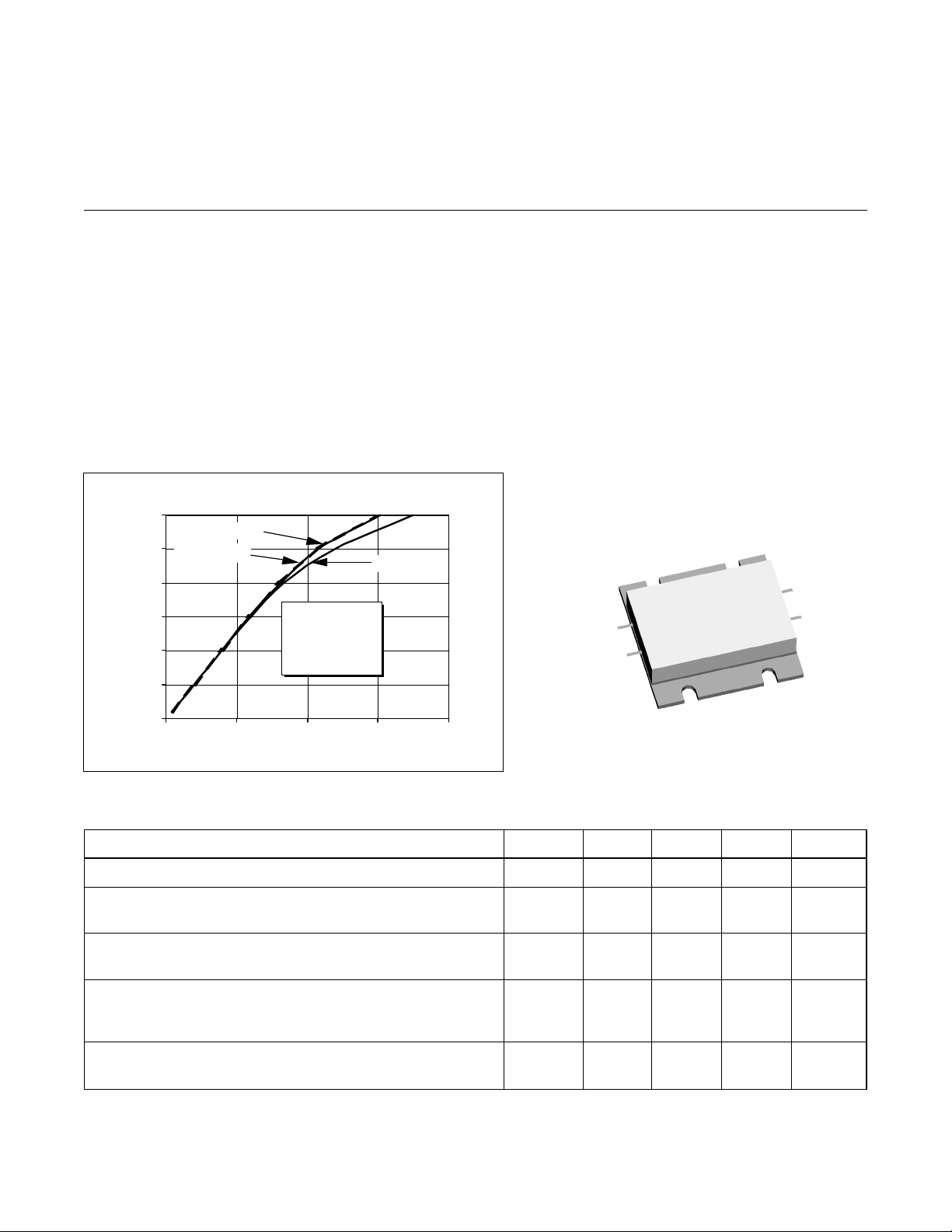
Typical Output Pow er vs. Input Pow er
30
25
20
f = 1.96 GHz
f = 1.93 GHz
f = 1.99 GHz
Performance at 1.930 to 1.990 GHz,
SUPPLY
= 26 V , V
V
- Power Gain = +24 dB Nom.
- Output Power = 25 Watts (P-1dB) Min
- Small Signal Flatness = ±0.2 dB Min
• Higher gain available with increased bias
voltages
• Optimum performance guaranteed with bias
voltages at 8.0 Volts
• Exceptional phase linearity and delay
characteristics
BIAS(1)
= 8.0 V , V
BIAS(2)
= 8.0 V
15
10
Output Power (Watts)
5
0
0.00 0.05 0.10 0.15 0.20
V
V
V
Input Power (Watts)
SUPPLY
BIAS(1)
BIAS(2)
= 26 V
= 8.0 V
= 8.0 V
e
32003
A-1234560015
Package J
Performance Characteristics
Parameter Symbol Min T yp Max Units
Frequency Range VDS (Nom.) = 26 f 1930 — 1990 MHz
Output Power at 1 dB Compressed
V
(Nom.) = 26, V
DS
Input VSWR
V
(Nom.) = 26, V
DS
Small Signal Gain
(Nom.) = 26 V , V
V
DS
I
Gain Flatness
V
= 270 mA, I
DQ(1)
(Nom.) = 26 V , V
DS
DQ(2)
BIAS(1)
BIAS(1)
BIAS(1)
= 360 mA
BIAS(1)
= 8.0 V , V
= 8.0 V , V
= 8.0 V , V
= 8.0 V , V
= 8.0 V P-1dB 25 30 — W
BIAS(2)
= 8.0 V y — 1.2:1 1.5:1 —
BIAS(2)
= 8.0 V , P
BIAS(2)
= 8.0 V — ±0.2 ±0.15 — dB
BIAS(2)
g
+23 +24 — dB
e
1
PTH 32003
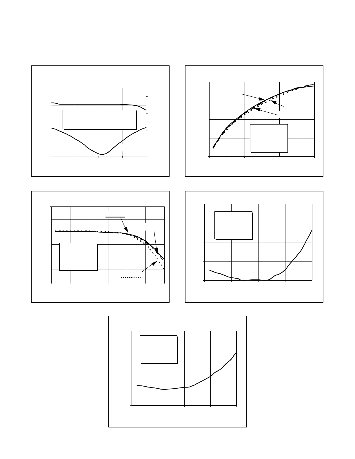
Typical Performance
e
Small Signal Gain and Return Loss
vs. Frequency
27
Smal l S i gnal Gai n
25
V
23
21
V
Small Signal Gain (dB)
19
1.86 1. 91 1. 96 2.01 2.06
SUPPLY
BIAS(1)
= 26 V
= 8.0 V, V
BIAS(2)
= 8.0 V
Return Loss
Frequency (GHz)
Power Gain vs. Power Out put
26
1.96 GHz
25
V
24
Power Gain (dB)
23
V
V
0 5 10 15 20 25 30
= 26 V
SUPPLY
= 8.0 V
BIAS(1)
= 8.0 V
BIAS(2)
Power Output (Watts)
1.99 GHz
6
2
-2
-6
-10
-14
-18
-22
-26
1.93 GHz
Return Loss (dB)
Power Added Efficiency vs. Output Power
40
f = 1.99 GHz
30
f = 1.93 GHz
20
V
SUPPLY
10
Power Added Efficiency (%)
0
0 5 10 15 20 25 30
V
V
BIAS(1)
BIAS(2)
f = 1.96 GHz
= 26 V
= 8.0 V
= 8.0 V
Output Power (W)
Phase Linearit y vs. Frequency
20
V
15
V
V
10
5
Phase Linearity (deg.)
0
1.85 1.90 1.95 2.00 2.05
= 26 V
SUPPLY
= 8.0 V
BIAS(1)
= 8.0 V
BIAS(2)
Frequency (GHz)
Small Signal Delay vs. Frequency
4.0
V
3.5
V
V
3.0
Delay (nS)
2.5
2.0
1.85 1. 9 1. 95 2 2. 05
SUPPLY
BIAS(1)
BIAS(2)
= 26 V
= 8.0 V
= 8.0 V
Frequency (GHz)
2
 Loading...