

PTF 102027
40 Watts, 925–960 MHz
GOLDMOS® Field Effect Transistor
Description
The PTF 102027 is a 40–watt GOLDMOS FET intended for EDGE
applications from 925 to 960 MHz. This device operates at 53%
efficiency with 15 dB of gain typical. Full gold metallization ensures
excellent device lifetime and reliability.
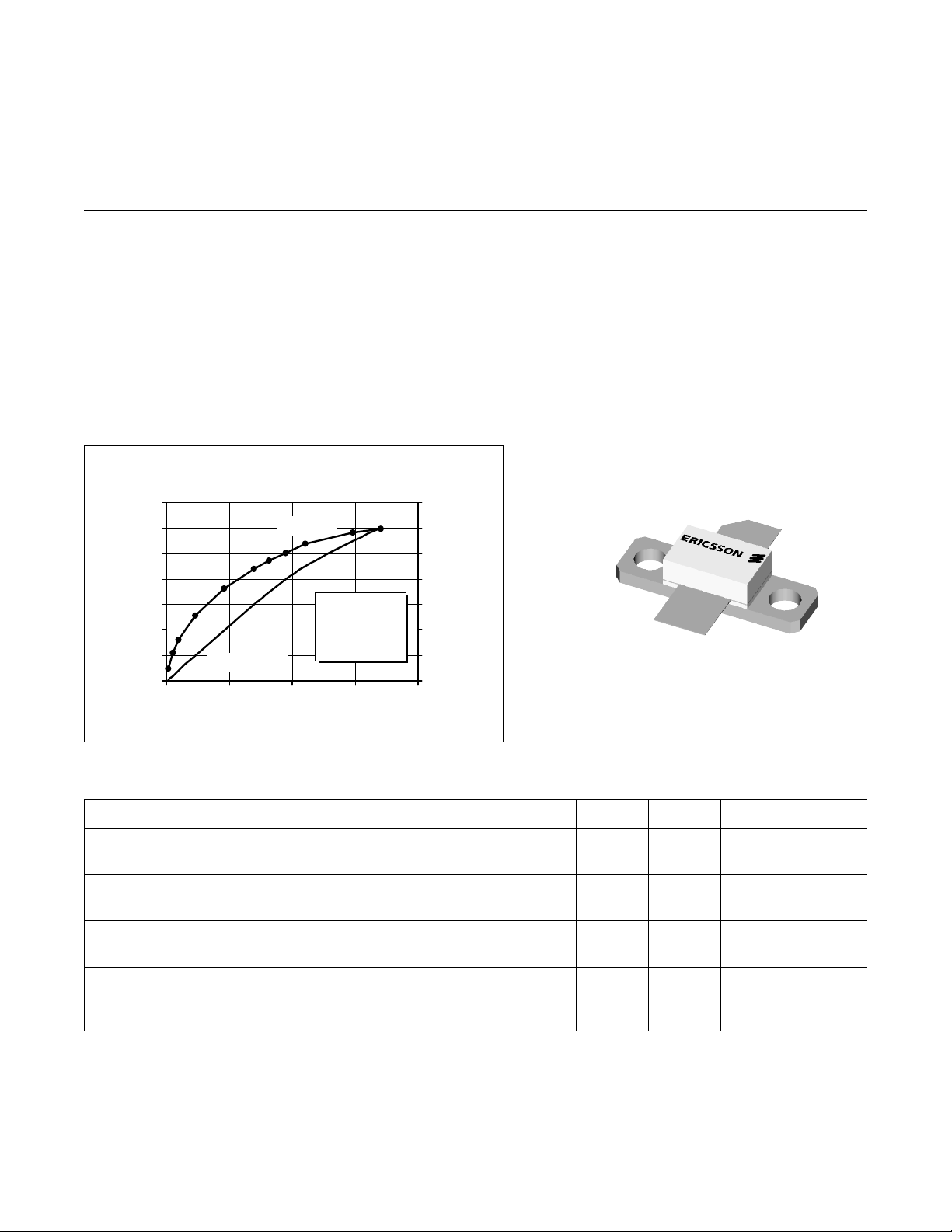
Typical Power Out put and Efficiency
vs. Input Pow er
70
60
50
40
30
20
10
Power Output (Watts)
0
0.0 0.5 1.0 1.5 2.0
Power Output
Input Power (Wa tts)
Efficiency
VDD = 26 V
I
f = 960 MHz
= 250 mA
DQ
70
60
50
40
30
20
Efficiency (%)
10
0
• Performance at 960 MHz, 26 Volts
- Output Power = 40 Watts
- Power Gain = 15.0 dB Typical
- Efficiency = 53% Typical
• Full Gold Metallization
• Excellent Thermal Stability
• 100% Lot Traceability
102027
1234560050
Package 20222
RF Specifications (100% Tested)
Characteristic Symbol Min Typ Max Units
Gain
(V
Power Output at 1 dB Compression
(V
Drain Efficiency
(V
Load Mismatch Tolerance
(V
—all phase angles at frequency of test)
All published data at T
= 26 V, P
DD
= 26 V, IDQ = 250 mA, f = 960 MHz) P-1dB 40 45 — Watts
DD
= 26 V, P
DD
= 26 V, P
DD
= 40 W, IDQ = 250 mA, f = 960 MHz) G
OUT
= 40 W, IDQ = 250 mA, f = 960 MHz) h 40 53 — %
OUT
= 40 W, IDQ = 250 mA, f = 960 MHz Y 10:1 — — —
OUT
= 25°C unless otherwise indicated.
CASE
pe
14.5 15 — dB
e
1
PTF 102027
e
Electrical Characteristics (100% Tested)
Characteristic Conditions Symbol Min Typ Max Units
Drain-Source Breakdown Voltage VGS = 0 V, ID = 25 mA V
(BR)DSS
Drain-Source Leakage Current VDS = 26 V, VGS = 0 V I
Gate Threshold Voltage VDS = 10 V, ID = 100 mA V
Forward Transconductance VDS = 5 V, ID = 3 A g
DSS
GS(th)
fs
65 ——Volts
——1.0 mA
3.0 — 5.0 Volts
— 2.0 — Siemens
Maximum Ratings
Parameter Symbol Value Unit
Drain-Source Voltage V
Gate-Source Voltage V
Operating Junction Temperature T
Total Device Dissipation P
DSS
GS
J
D
Above 25°C derate by 0.714 W/°C
Storage Temperature Range T
Thermal Resistance (T
= 70°C) R
CASE
STG
qJC
65 Vdc
±20 Vdc
200 °C
125 Watts
–40 to +150 °C
1.4 °C/W
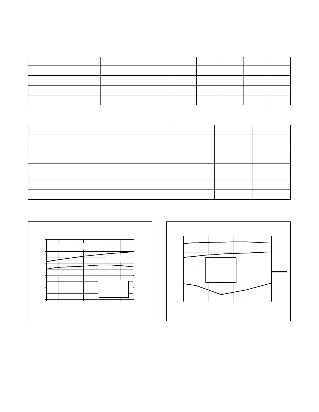
Typical Performance
Typical P
20
Outp ut P ower (W)
18
16
Gain
14
12
Gain (dB)
, Gain & Efficiency
OUT
vs. Frequency
VDD = 26 V
I
10
925 930 935 940 945 950 955 960
(at P-1dB)
Efficiency (%)
= 250 mA
DQ
Frequency (MHz)
70
60
50
40
30
20
Output Power & Efficiency
Broadband Test Fixture Performance
18
Gain
16
14
12
10
8
Gain (dB)
6
4
2
925 930 935 940 945 950 955 960
VDD = 26 V
= 250 mA
I
DQ
= 40 W
P
OUT
Frequency (MHz)
Efficiency
Return L oss (d B)
70
60
50
40
Efficiency (%)
30
20
-15
10
0
-30
Return Loss
-10
2
 Loading...