

Ericsson PTF10139 Datasheet
PTF 10139
60 Watts, 860-960 MHz
GOLDMOS® Field Effect Transistor
Description
The PTF 10139 is a GOLDMOS FET intended for amplifier applications to 860-960 MHz. This 60–watt device operates at 55% efficiency with 12.5 dB typical gain. Nitride surface passivation and full
gold metallization ensure excellent device lifetime and reliability.
Typical Output Pow er & Efficiency vs. Input Power
70
60
50
40
30
20
10
Output Power (Watts)
0
01234
Input Power (Wa tts)
Output Power
Efficiency
VDD = 28 V
I
= 500 mA
DQ
f = 960 MHz
80
70
60
50
40
30
20
10
Drain Efficiency (%) X
• Performance at 960 MHz, 28 Volts
- Output Power = 60 Watts Min
- Power Gain = 12.5 dB Typ
- Efficiency = 55% Typ
• Full Gold Metallization
• Silicon Nitride Passivated
• Excellent Thermal Stability
• Back Side Common Source
• 100% Lot Traceability
• Available in Package 20256 as PTF 10138
e
10139
A-1234561199
Also available in
Package
20256
Package
e
10138
A-1234562700
20251
RF Specifications (100% Tested)
Characteristic Symbol Min Typ Max Units
Common Source Power Gain
(V
Power Output at 1 dB Compression
(V
Drain Efficiency
(V
Load Mismatch Tolerance
(V
all phase angles at frequency of test)
All published data at T
= 28 V, P
DD
= 28 V, IDQ = 500 mA, f = 960 MHz) P-1dB 60 — — Watts
DD
= 28 V, P
DD
= 28 V, P
DD
= 60 W, IDQ = 500 mA, f = 960 MHz) G
OUT
= 60 W, IDQ = 500 mA, f = 960 MHz) h 50 55 — %
OUT
= 60 W, IDQ = 500 mA, f = 960 MHz— Y — — 10:1 —
OUT
= 25°C unless otherwise indicated.
CASE
ps
11.5 12.5 — dB
e
1
PTF 10139
e
Electrical Characteristics (100% Tested)
Characteristic Conditions Symbol Min Typ Max Units
Drain-Source Breakdown Voltage VGS = 0 V, ID = 25 mA V
(BR)DSS
Drain-Source Leakage Current VDS = 28 V, VGS = 0 V I
Gate-Source Leakage Current VGS = 20 V, VDS = 0 V I
Gate Threshold Voltage VDS = 10 V, ID = 75 mA V
Forward Transconductance VDS = 10 V, ID = 3 A g
DSS
GSS
GS(th)
fs
65 ——Volts
——1.0 mA
——1 mA
3.0 — 5.0 Volts
— 2.8 — Siemens
Maximum Ratings
Parameter Symbol Value Unit
Drain-Source Voltage V
Gate-Source Voltage V
Drain Current - Continuous I
Operating Junction Temperature T
Total Device Dissipation P
DS
GS
D
J
D
Above 25°C derate by 1.11 W/°C
Storage Temperature Range T
Thermal Resistance (T
= 70°C) R
CASE
STG
qJC
65 Vdc
±20 Vdc
7 Adc
200 °C
194 Watts
-65 to 150 °C
0.9 °C/W
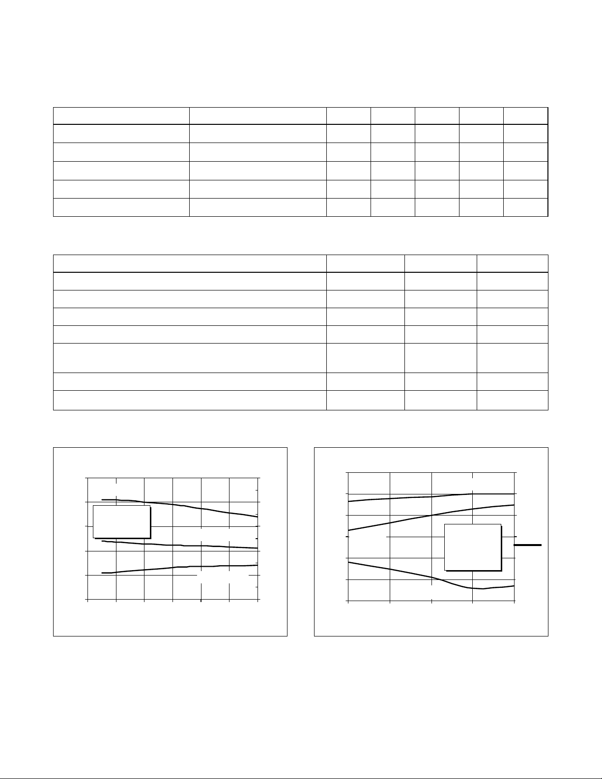
Typical Performance
Typical P
14
Gain (dB)
13
VDD = 28 V
12
I
DQ
Gain
11
10
9
840 860 880 900 920 940 960
, Gain & Efficiency
OUT
vs. Frequency
= 500 mA
Frequency (MHz)
Outp ut P ower (W)
(at P-1dB)
Efficiency (%)
90
80
70
60
50
Output Power & Efficiency
40
Broadband Test Fixture Perfor mance
14
13
12
11
Gain (dB)
Gain
10
9
8
920 930 940 950 960
Return Loss (dB)
Frequency (MHz)
Efficiency (%)
VDD = 28 V
= 500 mA
I
DQ
= 60 W
P
OUT
60
50
40
30
- 5
20
-15
10
-25
0
EfficiencyReturn Loss
2
 Loading...