

Ericsson PTF10125 Datasheet
PTF 10125
)
135 Watts, 1.4–1.6 GHz
GOLDMOS
™
Field Effect Transistor
Description
The PTF 10125 is an internally matched, common source N-channel
enhancement-mode lateral MOSFET intended for linear driver and
final applications from 1.4 to 1.6 GHz, such as DAB/DRB. It is rated
at 135 watts minimum power outpt. Nitride surface passivation and
full gold metallization ensure excellent device lifetime and reliability.
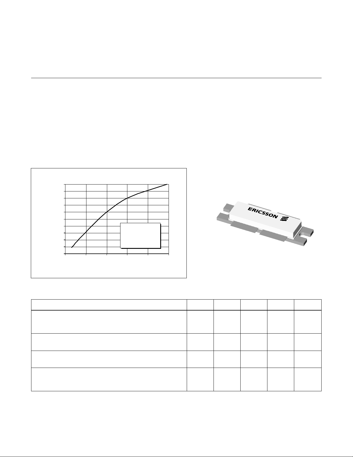
Typical Output Pow er vs. Input Power
200
180
160
140
120
100
80
60
40
Output Power (Watts
20
0
03691215
Input Power (Wa tts)
VDD = 28 V
I
= 1.3 A Total
DQ
f = 1500 MHz
INTERNALLY MATCHED
•
• Performance at 1.5 GHz, 28 V
- Output Power = 135 Watts Min
- Power Gain = 12.5 dB Typ
• Full Gold Metallization
• Silicon Nitride Passivated
• Back Side Common Source
• Excellent Thermal Stability
• 100% Lot Traceability
10125
A-1234569935
Package 20250
RF Specifications (100% Tested)
Characteristic Symbol Min Typ Max Units
Gain
(V
f = 1.50, 1.55 GHz)
Power Output at 1 dB Compression
(V
Drain Efficiency
(V
Load Mismatch Tolerance
(V
—all phase angles at frequency of test)
All published data at T
= 28 V , P
DD
= 28 V, IDQ = 1.3 A Total, f = 1.50, 1.55 GHz) P-1dB 135 150 — Watts
DD
= 28 V, P
DD
= 28 V, P
DD
= 30 W, IDQ = 1.3 A Total, G
OUT
= 135 W, IDQ = 1.3 A Total, f = 1.5 GHz) h
OUT
= 67.5 W, IDQ = 1.3 A Total, f = 1.5 GHz Y — — 10:1 —
OUT
= 25°C unless otherwise indicated.
CASE
ps
D
11.5 12.5 — dB
35 40 — %
e
1
PTF 10125
y
y
s
e
Electrical Characteristics (100% Tested—characteristics, conditions and limits shown per side)
Characteristic Conditions Symbol Min Typ Max Units
Drain-Source Breakdown Voltage VGS = 0 V , ID = 100 mA V
(BR)DSS
Zero Gate Voltage Drain Current VDS = 28 V , VGS = 0 V I
Gate Threshold Voltage VDS = 10 V , ID = 150 mA V
Forward Transconductance VDS = 10 V , ID = 6 A g
DSS
GS(th)
fs
65 — — Volts
— — 5.0 m A
3.0 — 5.0 Volts
2.0 4.0 — Siemens
Maximum Ratings
Parameter Symbol Value Unit
Drain-Source Voltage
Gate-Source Voltage
Operating Junction Temperature T
Total Device Dissipation P
Above 25°C derate by 2.51 W/°C
Storage Temperature Range T
Thermal Resistance (T
(1)
per side
(1)
(1)
= 70°C) R
CASE
V
V
DSS
GS
J
D
STG
qJC
65 Vdc
±20 Vdc
200 °C
440 Watts
–40 to +150 °C
0.39 °C/W
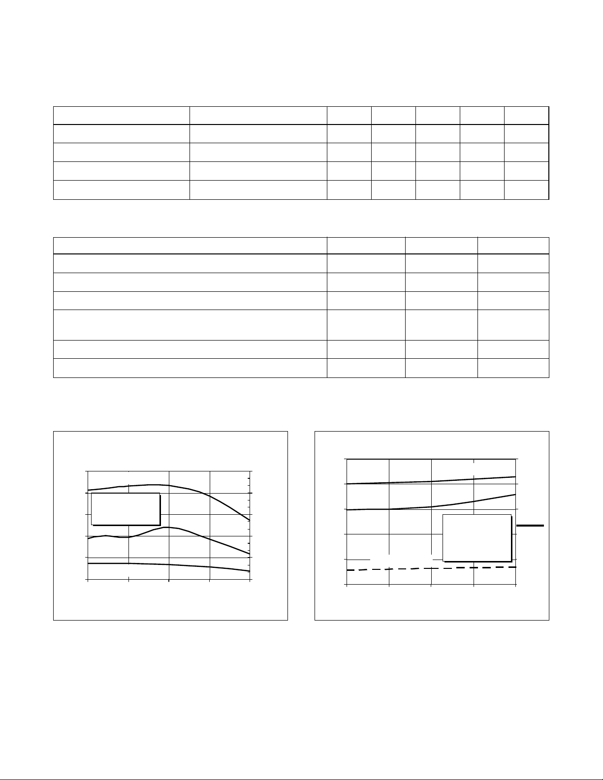
Typical Performance
Typical P
, Gain & Efficiency
OUT
vs. Frequency
17
Outp ut P ower (W)
16
VDD = 28 V
15
14
Gain (dB)
13
12
= 1.3 A Tota l
I
DQ
Efficiency (%)
1400 1450 1500 1550 1600
Gain (dB)
Frequency (MHz)
(at P-1dB)
180
150
120
90
60
Output Power & Efficienc
30
Gain (dB)
Broadband Test Fixture Performance
16
Efficiency (%)
14
Gain
12
VDD = 28 V
10
8
6
1450 1475 1500 1525 1550
Return L oss (d B )
Frequency (MHz)
= 1.3 A Tota l
I
DQ
= 135 W
P
OUT
-10
-15
-20
50
40
30
20
10
0
Efficienc
Return Los
2
 Loading...