

Ericsson PTF10122 Datasheet
PTF 10122
)
50 Watts WCDMA, 2.1–2.2 GHz
GOLDMOS
™
Field Effect T ransistor
Description
The PTF 10122 is an internally matched common source N-channel
enhancement-mode lateral MOSFET intended for WCDMA applications
from 2.1 to 2.2 GHz. It is rated at 50 watts power output, with 11 dB of
gain. Nitride surface passivation and full gold metallization ensure excellent device lifetime and reliability.
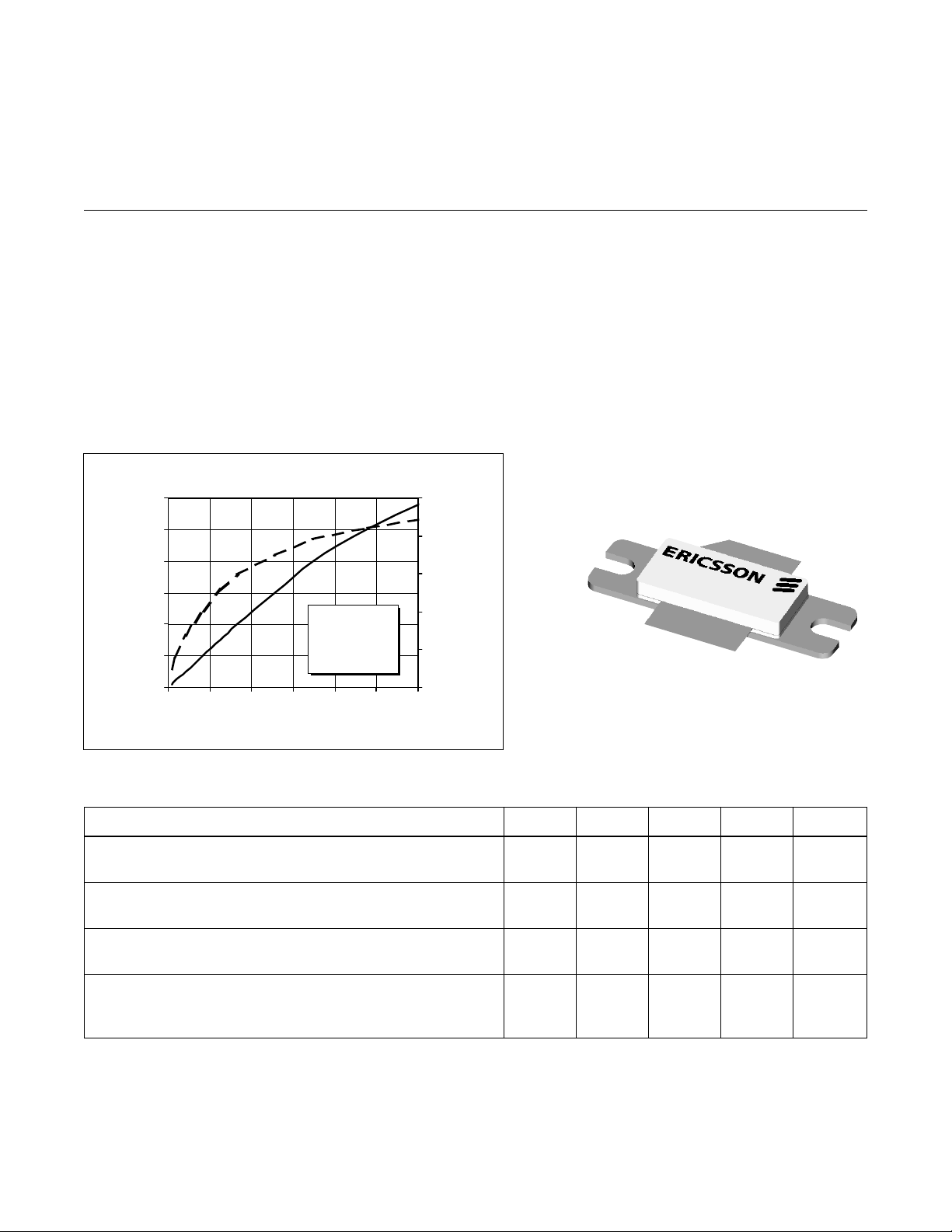
Typical Output Pow er vs. Input Pow er
60
50
40
30
20
10
Output Power (Watts)
0
0123456
Input Power (Wa tts)
VDD = 28 V
= 600 mA
I
DQ
f = 2.17 GHz
50
40
30
20
Efficiency (%
10
0
INTERNALLY MA TCHED
•
• Guaranteed Performance at 2.17 GHz, 28 V
- Output Power = 50 Watts Min
- Gain = 11.0 dB Typ
- Efficiency = 35% Typ
• Full Gold Metallization
• Silicon Nitride Passivated
• Back Side Common Source
• Excellent Thermal Stability
• 100% Lot Traceability
10122
A-1234569946
Package 20248
RF Specifications (100% T ested)
Characteristic Symbol Min T yp Max Units
Gain
(V
Power Output at 1 dB Compression
(V
Drain Efficiency
(V
Load Mismatch Tolerance
(V
—all phase angles at frequency of test)
All published data at T
= 28 V, P
DD
= 28 V , IDQ = 600 mA, f = 2.17 GHz) P-1dB 50 — — Watts
DD
= 28 V , P
DD
= 28 V , P
DD
= 15 W, IDQ = 600 mA, f = 2.1 1 GHz) G
OUT
= 50 W, IDQ = 600 mA, f = 2.17 GHz) h
OUT
= 50 W, IDQ = 600 mA, f = 2.17 GHz Y — — 10:1 —
OUT
= 25°C unless otherwise indicated.
CASE
ps
D
10.0 11.0 — dB
30 35 — %
e
1
PTF 10122
y
)
)
e
Electrical Characteristics (100% T ested)
Characteristic Conditions Symbol Min Typ Ma x Units
Drain-Source Breakdown Voltage VGS = 0 V , ID = 100 mA V
(BR)DSS
Zero Gate Voltage Drain Current VDS = 28 V , VGS = 0 V I
Gate Threshold Voltage VDS = 10 V , ID = 150 mA V
Forward Transconductance VDS = 10 V , ID = 2 A g
DSS
GS(th)
fs
65 — — Volts
— — 2.0 mA
3.0 — 5.0 Volts
— 4.0 — Siemens
Maximum Ratings
Parameter Symbol Value Unit
Drain-Source Voltage V
Gate-Source Voltage V
Operating Junction T emperature T
T otal Device Dissipation P
DSS
GS
J
D
Above 25°C derate by 1.35 W/°C
Storage T emperature Range T
Thermal Resistance (T
= 70°C) R
CASE
STG
qJC
65 Vdc
±20 Vdc
200 °C
237 Watts
–40 to +150 °C
0.74 °C/W
Typical Performance
Typical P
12
11
Gain (dB)
10
Gain
9
VDD = 28 V
8
I
7
2000 2100 2200 2300
, Gain & Efficiency
OUT
vs. Frequency
= 600 mA
DQ
Frequency (MHz)
(at P-1dB)
Outp ut P ower (W)
Efficiency (%)
Broadband Test Fixture Performance
14
70
60
50
40
30
Output Power & Efficienc
20
13
12
11
10
Gain (dB)
9
8
7
6
2100 2125 2150 2175 2200
Gain
Efficiency @ P-1dB
VDD = 28 V
= 600 mA
I
DQ
= 15 W
P
OUT
Frequency (MHz)
Return Loss
50
40
30
Efficiency (%
0
20
- 5
-10
10
-15
-20
-25
0
Return Loss (dB
2
 Loading...