

Ericsson PTF10119 Datasheet
PTF 10119
12 Watts, 2.1–2.2 GHz
GOLDMOS
™
Field Effect Transistor
Description
The PTF 10119 is an internally matched, common source, N-channel
enhancement-mode lateral MOSFET intended for WCDMA
applications from 2.1 to 2.2 GHz. It is rated at 12 watts power output.
Nitride surface passivation and gold metallization ensure excellent
device reliability.
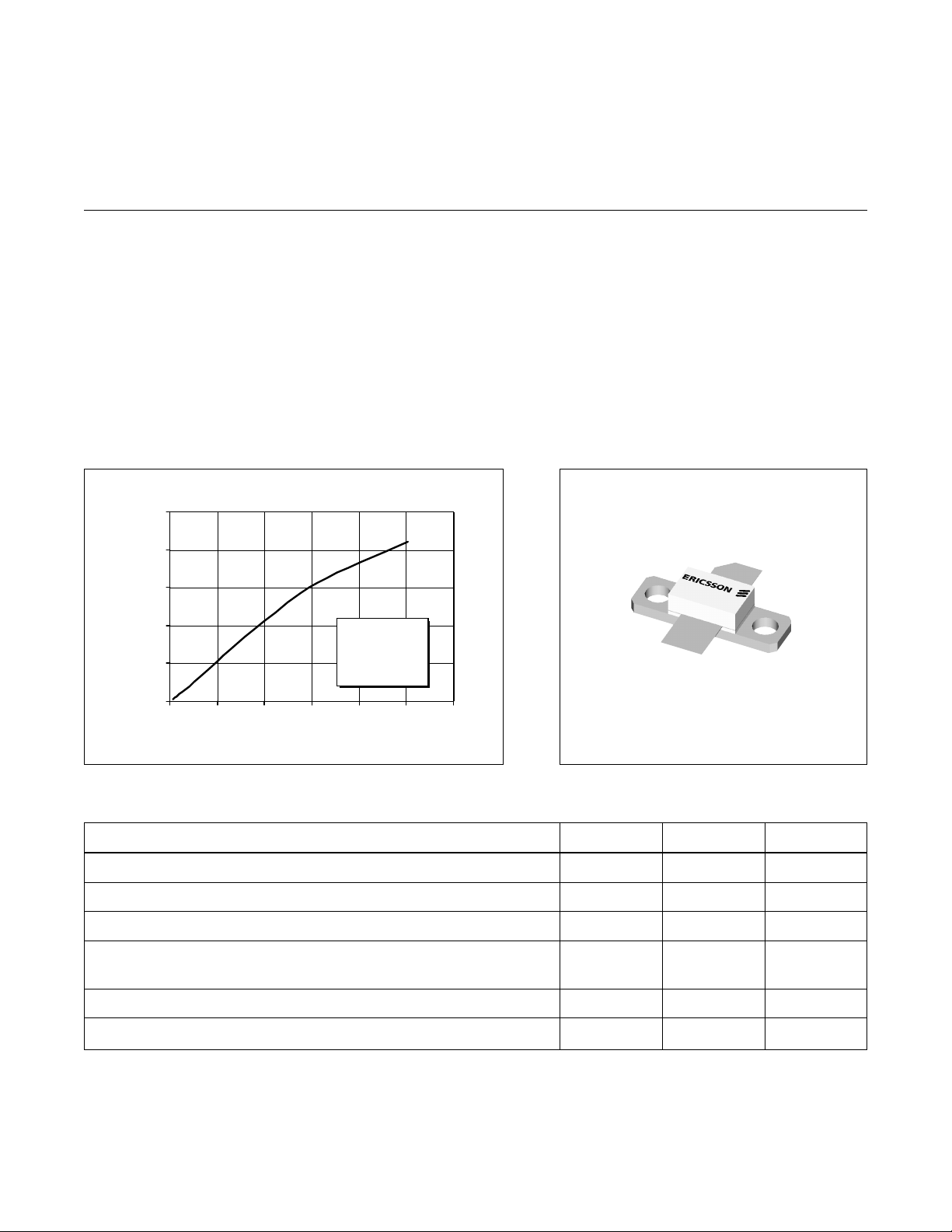
Typical Output Pow er vs. Input Pow er
20
16
12
•
INTERNALLY MATCHED
• Performance at 2.17 GHz, 28 Volts
- Output Power = 12 Watts Min
- Power Gain = 11 dB Typ
- Efficiency = 43% Typ @ P-1dB
• Full Gold Metallization
• Silicon Nitride Passivated
• Back Side Common Source
• Excellent Thermal Stability
• 100% lot traceability
10119
A-1234560053
8
4
Output Power (Watts)
0
0 0.2 0.4 0.6 0.8 1 1.2
Input Power (Wa tts)
VDD = 28 V
= 160 mA
I
DQ
f = 2170 MHz
Package 20222
Maximum Ratings
Parameter Symbol Value Unit
Drain-Source Voltage V
Gate-Source Voltage V
Operating Junction Temperature T
Total Device Dissipation at T
Above 25°C derate by 0.31 W/°C
Storage Temperature Range T
Thermal Resistance (T
flange
= 25°C P
flange
= 70°C) R
DSS
GS
J
D
STG
qJC
65 Vdc
±20 Vdc
200 °C
55 Watts
–40 to +150 °C
3.2 °C/W
e
1
PTF 10119
0
W
A
V
E
L
e
Electrical Characteristics (100% Tested)
Characteristic Conditions Symbol Min Typ Max Units
Drain-Source Breakdown Voltage VGS = 0 V , ID = 50 mA V
(BR)DSS
Zero Gate Voltage Drain Current VDS = 26 V , VGS = 0 V I
Gate Threshold Voltage VDS = 10 V , ID = 75 mA V
Forward Transconductance VDS = 10 V , ID = 2 A g
DSS
GS(th)
fs
65 — — V olts
— — 1.0 mA
3.0 — 5.0 Volts
— 0.8 — Siemens
RF Specifications (100% Tested)
Characteristic Symbol Min Typ Max Units
Gain
(V
Power Output at 1 dB Compressed
(V
Drain Efficiency
(V
Load Mismatch Tolerance
(V
—all phase angles at frequency of test)
= 28 V, P
DD
= 28 V, IDQ = 160 mA, f = 2.17 GHz) p-1dB 12 14 — Watts
DD
= 28 V, P
DD
= 28 V, P
DD
= 3 W, IDQ = 160 mA, f = 2.11, 2.17 GHz) G
OUT
= 12 W, IDQ = 160 mA, f = 2.17 GHz) h
OUT
= 12 W, IDQ = 160 mA, f = 2.17 GHz Y — — 10:1 —
OUT
ps
D
10 11 — dB
30 43 — %
Impedance Data
5
4
.
0
VDS = 28 V, P
= 12 W, IDQ = 160 mA
OUT
D
Z Source Z Load
Z0 = 50 W
3
.
0
2
.
0
G
0.3
2.30 GHz
0.5
0.4
1
.
S
Frequency Z Source W Z Load W
GHz R jX R jX
0
2.30 GHz
0
.
0
Z Load
2.00 GHz
0.1
0.2
2.00 5.7 -12.11 3.30 1.21
2.10 16.4 -19.50 3.55 0.92
2.12 19.7 -18.82 4.12 0.88
2.15 22.8 -14.14 3.75 0.62
1
.
0
-
-
<
2
.
0
Z Source
2.00 GHz
2.17 23.0 -13.15 3.53 0.34
2.20 26.6 -9.28 3.32 0.38
2.30 20.2 12.03 3.23 0.84
3
.
0
5
2
 Loading...