

Page 1
October 1998
PBM 990 08/1MQ
ATM Multi Service Chip
Description
The ATM Multi Service Chip is a cost efficient solution
for multi service access applications. It is especially
suited for ADSL, VDSL, FTTx and HFC applications,
where all services are transported over ATM.
The chip interfacesto the modem/transceiver chip
set, and distributes data to and from the different
service interfaces. The integrated services are ATM
Forum 25.6 and POTS/ISDN. Other services such as
Ethernet can be added via the Utopia interface.
Circuit emulation via AAL1 is performed for the
POTS/ISDN service.
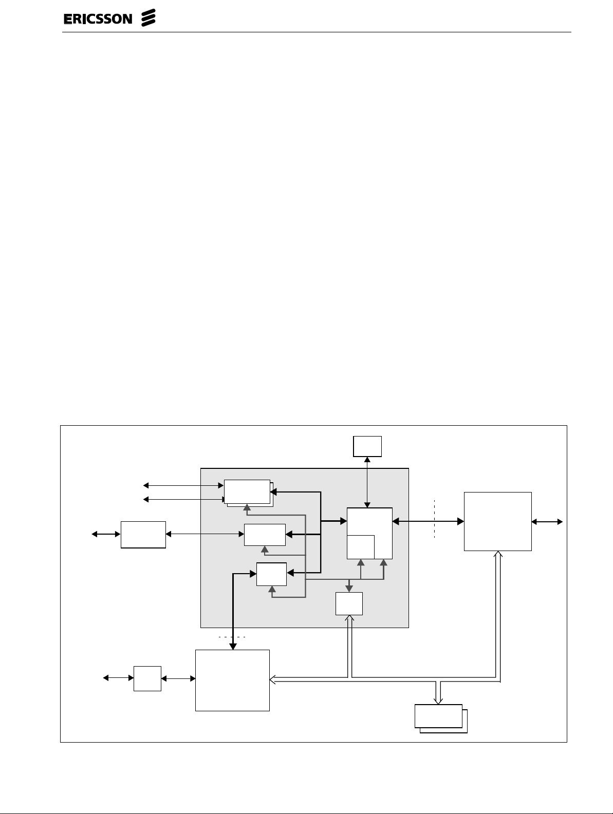
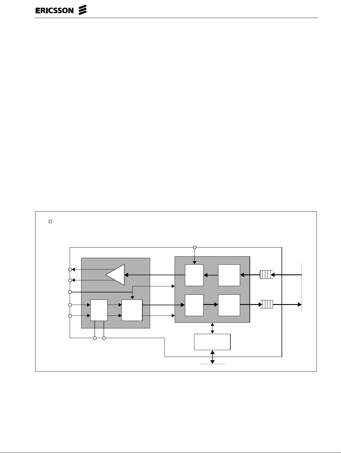
ATM Multi Service Chip
ATMF 25.6 #2
POTS
ATMF 25.6 #1
circuitry
Line
PCM
ATMF
transceiver
Circuit
emulation
Key Features
• Low power CMOS technology.
• 240-pin MQFP package.
• Utopia level 2 interface to modem/transceiver.
• Programmable VPI/VCI handling.
• Upstream QoS handling supporting up to 128
kBytes external SRAM.
• Generic CPU interface.
• Support for ATM signalling and OAM via CPU.
• Performance monitoring counters.
• Two ATM Forum 25.6 interfaces.
• Utopia level 1/2 interface for additional external
services.
• POTS/ISDNover ATM via AAL1, PCM interface for
up to 4 structured 64 kbps channels or E1/T1
interface for one unstructured 2048/1544 kbps
channel.
QoS
buffer
Utopia2
Utopia 2
ATM
Core
Cell
buffer
Modem /
Transceiver
10Base-T
Utopia 1/2
E/N
xcvr
CPU
Figure 1. Block diagram.
Utopia
buffer
CPU
block
CPU bus
Memory
1 (14)
Page 2
PBM 990 08/1MQ
Functional description
General
The Multi Service Chip handles the distributionof ATM
traffic in multi service access applications, and is
especially suited for Network Terminals (NT). All
functions are implemented in hardware only. The chip
hasaUtopialevel2interfaceto the modem/transceiver
chip set and several different service interfaces. The
service interfaces include two ATMF 25.6 Mbps
interfaces, a PCM interface that supports circuit
emulation for four structured 64 kbps channels, and a
Utopia level 2 (or level 1) interface. The PCM interface
can also be configured to a digital E1/T1 interface
which supports circuit emulation for an unstructured
2048/1544 kbps channel.
By setting up ATM connections via the CPU interface,
the Multi Service Chip will distribute data traffic
between the different service interfaces and the
modem/transceiver interface. Since all functions are
implemented in hardware only, the Multi Service Chip
can handle very high bandwidth in both the
downstream direction (from the modem/transceiver
interface to the service interfaces) and the upstream
direction (from the service interfaces to the
modem/transceiver interface).
In the upstream direction, data might arrive on the
tributary interfaces at higher bit rate than the
modem/transceiver can handle. Therefore the Multi
Service Chip has an interface to an external SRAM for
temporary storage of upstream data. The interface
supports SRAM with sizesupto 128 kBytes, which can
be divided into 4 different buffer areas. This enables
support for different service classes.
Beside the connections between the
modem/transceiver interface and the service
interfaces,itisalsopossibletosetupATMconnections
between the CPU and both the modem/transceiver
interface and the service interfaces. This makes it
possible to let the NT have an active role in signalling
and OAM.
ATM Core
The ATM Core is the central block of the Multi Service
Chip. It handles the distribution of ATM cells between
the modem/transceiver interface (also referred to as
the
aggregate
the integrated service devices (also referred to as the
tributary
routingand translation, and has aset of VPI/VCI tables
that must be configured by the CPU. The structure is
shown in Figure 2.
interface) and the internal interface to
interface). This block handles the VPI/VCI
Tx_Utopia
Tributary
(Service)
Rx_Utopia
CPU bus
CPUuw
Figure 2. Structure of ATM Core.
Mux
VPI/VCI
configuration
VPI/VCI
demux and
translation
CPUur
Loop back
EPD
CPUdw
CPUdr
QoS1
QoS2
QoS3
QoS4
VPI/VCI
demux and
translation
Loop back
VPI/VCI
configuration
Mux
Rx_Utopia
Aggregate
(Modem)
Tx_Utopia
2 (14)
Page 3
PBM 990 08/1MQ
Data flows
In the downstream direction, ATMcells are distributed
from the aggregate interface to either one of the
tributary services, the CPU buffer, or the aggregate
loop-back buffer where they will be send back
upstream.The destination of the cells is determined by
the VPI/VCI tables.
When no cells are distributedto the tributary interface,
cells can be read from either the CPUdw buffer or the
tributary loop-back buffer. No VPI/VCI handling is
performedforthese cells. The CPUdw bufferis divided
into three separate buffers, where each is associated
withoneoftheATMFand Utopia blocks.Theloop-back
buffercanbe associated with any of the service blocks.
In the upstream direction, ATM cells are distributed
from the tributary interface to either one of the QoS
buffers, the CPUur buffer, or the tributary loop-back
buffer where they will be send back downstream. The
destination of the cells is determined by the VPI/VCI
tables. As for the downstream direction the CPUur
buffer is divided into three separate buffers, where
each is associated with one of the ATMF and Utopia
blocks. Besides the tributary interface, cells can also
be read from the CPUuw buffer and sent to one of the
QoS buffers. No VPI/VCI handling is performed for
these cells. The CPUuw buffer can be associated with
any of the QoS buffers.
Cells are distributed from the QoS buffers and the
aggregate loop-back buffer to the aggregate interface.
The QoS buffers can be configured to have different
priorities. As an example, all four QoS buffers can be
associated with only one channel at the aggregate
interface,withfourdifferentpriorities. It is alsopossible
to associate two buffers with one channel and two with
another,orassociate all buffers with one channel each.
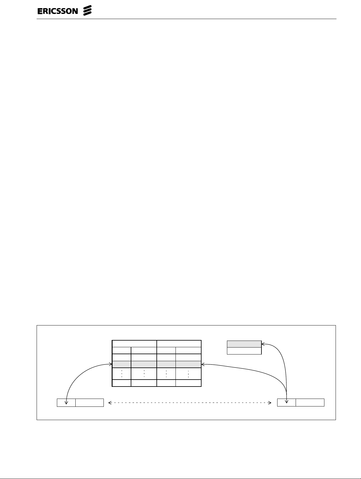
VPI/VCI handling
TheATMCore handles VPI/VCI routing and translation
of upstream and downstream cells separately. This
means that the CPU must set up one set of
connections for the downstream direction and another
for the upstream direction. For each direction, a
maximum of 128 simultaneous connections are
supported.
In the downstream direction, the VPI/VCI tables
support the 4 least significant bits of the VPI, which
gives a VPI range from 0 to 15. In addition to this, the
8 most significant bits of the VPI is defined in a
separate register. This means that the VPI can have
different ranges in steps of 16, e.g. 0-15, 16-31, 4080-
4095. All cells with VPI values outside the chosen VPI
range will be discarded. Beside these 16 VP’s, a
broadcastVPcanalsobesetupbyaseparateregister.
Cellswith a VPI that corresponds to thisregister will be
sent to the CPU.
In the upstream direction, the VPI/VCI tables also
support the 4 least significant bits of the VPI, which
gives a VPI range from 0 to 15.
For both upstream and downstream direction, the
VPI/VCItablessupport the 8 leastsignificantbits of the
VCI, which gives a VCI range from 0 to 255.
Any of the 128 connections for each direction can be
configured as either a VP cross connection (VPC) or a
VC cross connection (VCC). VPC means that only the
VPI determines the destination of the cell, and the VCI
is transparent. In this case only the VPI is translated.
VCC means that also the VCI determines the
destination, and in this case both VPI and VCI are
translated. The VPI/VCI handling is shown in Figure 3
and Figure 4.
Demux and translation table
Tributary cell
Tributary
VPI[3:0] VCI[7:0]
0
X
127
-
VP cross connection; VC transparent except for OAM
Aggregate
VPI[3:0]VCI[7:0]
Y
Figure 3. VP cross connection through ATM Core.
VP filter
Range[11:4]
Broadcast[11:0]
-
Aggregate cell
3 (14)
Page 4
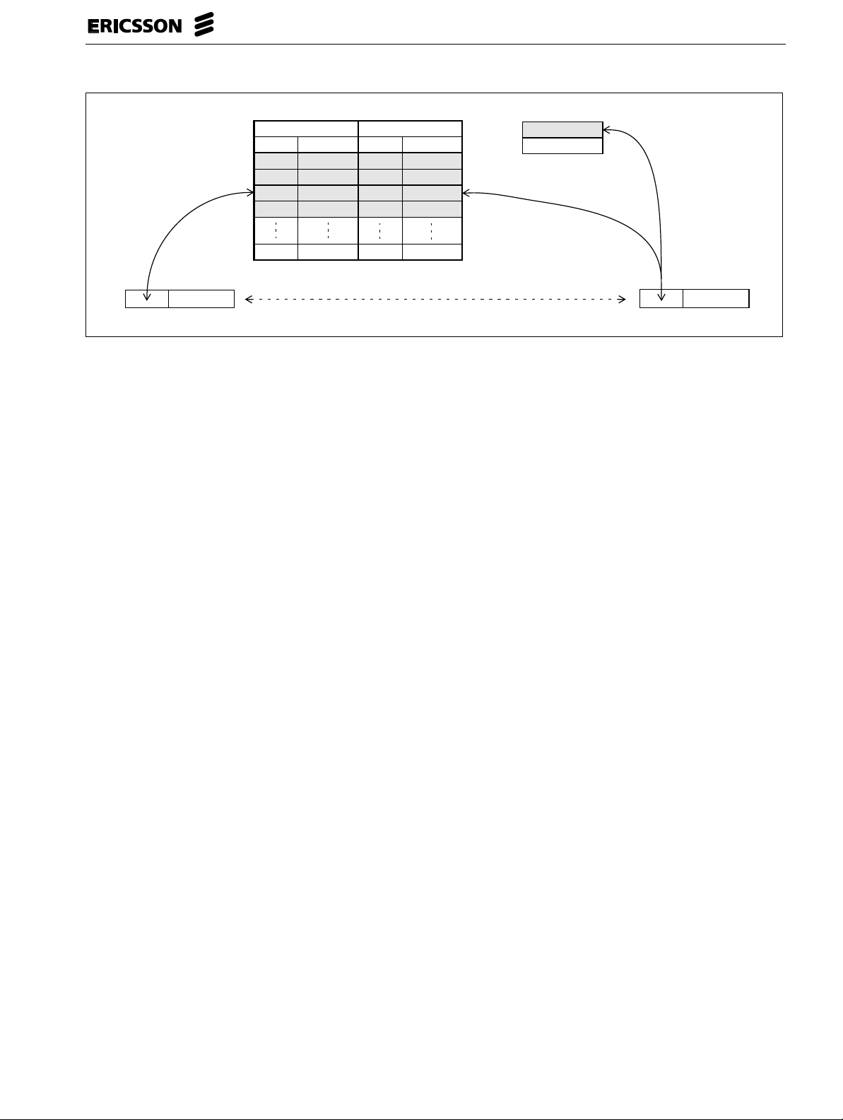
PBM 990 08/1MQ
Demux and translation table
Tributary cell
Tributary
VPI[3:0] VCI[7:0]
5
16
A
C
VC cross connection; All VC’s must be set up except for OAM
127
0
X
X
X
X
Aggregate
VPI[3:0]VCI[7:0]
Y
Y
Y
Y
Figure 4. VC cross connection through ATM Core.
Operation and Maintenance (OAM) handling
For all connections that are set up through ATM Core,
F4 and F5 OAM cells will be sorted out and sent to the
CPU automatically. For VPC’s, only the F4 segment
and end-to-end cells are sorted out. For VCC’s,the F4
cells are handled just like for VPC’s, but the F5
segment cells are also sorted out.
VP filter
Range[11:4]
Broadcast[11:0]
5
16
B
D
Aggregate cell
Performance monitoring
There are a number of counters in the ATM Core that
can be used for performance monitoring, such as
downstream user cell counter,upstream user cell
counter,EPDeventcounter
(
PPD) event counter
.
and
PartialPacketDiscard
Since the OAMflow is terminated in the ATM Core, it is
possible to re-generate it by letting the CPU create
OAM cells and write them into the CPU buffers for
further downstream or upstream transportation.
Quality of Service (QoS) handling
QoS buffering is performed for the upstream direction
using an external SRAM with sizes up to 128 kBytes.
The buffer can be divided into 4 (or less) different
areas, which can be configured to have different
priorities when they are read at the aggregate
interface. The size of each buffer area is configurable.
Any upstream ATM connection between the tributary
interface and the QoS buffer might be subject to Early
Packet Discard (EPD). For this a threshold value per
QoS buffermust be configured, to which the amount of
data in the buffer is compared.
ATMF 25.6 service
The two integrated ATMF 25.6 transceivers include all
the TC and PMD layer functions as specified in ref[1].
They are optimized to be connected to the PE-67583
transformer from Pulse Electronics.
Since there are two ATMF devices in the Multi Service
Chip, it is possible to set up broadcast connections to
both ATMF devices. This means that such ATM cells
will be accepted and distributed through both devices.
Itis also possible to transfertiming information overthe
ATMF interfaces. In this case an 8 kHz reference clock
must be provided from the modem/transceiver, as
shown in the block diagram in Figure 5.
The functions in the data paths are described below.A
number of performance monitoring counters are also
included.
4 (14)
Page 5
PBM 990 08/1MQ
Transmit path
The ATM Core transmits cells to the ATMF device over
the internal Utopia interface, which are stored in the
two cell deep
The
Tx Cell Processor
FIFO and calculates a newHEC byte which is inserted
inthe cell header. When no cells are availablein the Tx
FIFO, idle cells are generated and transmitted.
The
Framer
of the cell flow, and inserts a command byte (X_X or
X_4)at the startof each cell. Each timea positive edge
is detected on the 8 kHz reference clock
(NET_REF_CLK), a timing information byte (X_8) is
inserted in the data flow. Finally the data is serialized
and NRZI encoded.
The analog
a bipolar format and transmits it on the external
outputs.
Tx FIFO
.
reads the cells from the Tx
performs scrambling and 4B5B encoding
Line Driver
converts the data stream into
Receive path
The analog data is passed through the
where the high frequency noise is removed and the
data is equalized in order to compensate for the line
distortion.
The analog data is converted to a digital format in the
Data & Clock Recovery
block, which also recovers
the receive clock from the data stream.
The
Deframer
aligns the cell stream by detecting the
command bytes (X_X or X_4). All other command
bytes are sorted out, and the data is 5B4B decoded
and descrambled before it is forwarded. Cells with one
or several faulty 5-bit symbols are discarded.
The
Rx Cell Processor
calculates the HEC value of
the cell header and discards cells with a faulty header.
Idle cells and physical OAM cells are also sorted out.
The remaining correct data cells are stored in the two
cell deep
Rx FIFO
.
Cells are read from the Rx FIFO by the ATM Core over
the tributary Utopia interface.
Equalizer
= external ports
ATMF transceiver
PMD
ATMFx_TXD_X
ATMFx_TXD_Y
ATMF_CLKT_32
ATMFx_RXD_X
ATMFx_RXD_Y
Equa-
lizer
ATMFx_EQ_A
Line
Driver
ATMFx_EQ_B
Data &
Clock
Recovery
Figure 5. ATMF transceiver block diagram.
Tx Clk
Rx Clk
NET_REF_CLK
Framer
De-
framer
Configuration &
Status Registers
TC
Tributary
Utopia
Tx FIFO
Tx Cell
Processor
Rx FIFO
Rx Cell
Processor
CPU interface
5 (14)
Page 6

Telephony service (POTS/ISDN)
For POTS/ISDN, the Circuit Emulation (CE) block
handles adaptation between ATM and synchronous
timeslot based data. It is AAL1 based and takes care
of the segmentation and reassembly handling
including functions such as data over- and underflow,
and lost and misinserted cells according to ref[2].
The external interface can be configured as either
PCM or digital E1/T1 (i.e. data and clock). There are
five different modes of operation:
•
Basic PCM mode
structured 64 kbps channels without CAS. Only the
data from one 64 kbps channel is mapped into one
AAL1 channel, where the cells can be either totally
filledor partiallyfilled with 22 or11 bytes.Signalling
can be handled by the CPU in a separate ATM
channel as shown in Figure 6.
•
PCM_E1 mode
64 kbps channels including CAS. The data from
one 64 kbps channel as well as the corresponding
CASinformationismapped into one AAL1 channel.
This is compliant with ref[3].
, which handles up to 4
, which handles up to 4 structured
PBM 990 08/1MQ
•
PCM_T1 mode
64 kbps channels including CAS. The data from
one 64 kbps channel as well as the corresponding
CASinformationismapped into one AAL1 channel.
This is compliant with ref[3].
•
E1 mode
kbps channel.
•
T1 mode
kbps channel.
Inorderto synchronizethe telephonyservice, an 8 kHz
referenceclockis neededfromthemodem/transceiver.
An external clock is also needed, from which the
telephony clock is extracted and locked to the
reference clock.
There are a number of counters in the CE block that
can be used for performance monitoring, such as
cells counters,data under- and overflow counters
out of synchronization counters
, which handles up to 4 structured
, which handles one unstructured 2048
, which handles one unstructured 1544
lost
, and
.
Network Terminal
MSC
PCM
Line
circuitry
Control
Figure 6. Signalling handling in basic PCM mode.
CE
CPU
AAL5 SAR
POTS
signalling
AAL1 VCC
AAL1 VCC
8 kHz reference
ATM Core
AAL5 VCC
CPU bus
Modem
Utopia
Copper
Coax
Fiber
6 (14)
Page 7

PBM 990 08/1MQ
Utopia service
The Utopia service interface is a slave interface that
can be configured to work in both level 1 and level 2
modes. In level 2 mode, the Utopia address can be
configured to any value between 0 and 30.
Basically, the Utopiaservice interfaceblockconsistsof
a two cell deep FIFO in each direction, which converts
between the data rates of the ATM Core and the
external device that will be connected to the MSC.
The Utopia service interface makes it easy to add
services besides ATMF and POTS/ISDN. For example
it can be connected to an external AAL5 device for
Ethernet or USB services.
CPU interface
The CPU interface is used for two main tasks. One is
that the CPU must configure the Multi Service Chip
including the VPI/VCI tables. If performance
monitoring is wanted, the different counters must also
be read continuously. The other task is that the CPU
might need to write and read ATM cells to and from the
ATM Core.
Since the second task might be timing critical
(especially for downstream cells), the CPU interface
uses a 16-bit bidirectional data bus. In order to make
the handling of the cell header more efficient in the
CPU, the HEC byte is skipped. This means that the
CPUalwaysreadsandwrites only 52 bytespercell(26
read or write cycles).
The CPU interface includes an interrupt signal, which
is asserted when certain events occur in the Multi
Service Chip.Sucheventsare CPU cellavailable in the
ATM Core, and data overflow, underflow and out of
synchronization in the CE block. Any of these interrupt
eventscan be inhibited with an
interrupt mask register
.
Other signals on the CPU interface are a 12-bit
address bus, chip select, data acknowledge, and
output enable.
7 (14)
Page 8

Signal description
The signal interfaces are described below and shown
in Figure 7.
NET_REF_CLK
ATMF_CLKT_32
PBM 990 08/1MQ
QoS interface
ATMF
interfaces
CE_CLK
ATMF
transceiver
Telephony
interface
Test (JTAG)
Service Utopia
interface
Figure 7. Signal interfaces.
Clocks and reset
MSC_SYS_CLK (input)
This is the system clock that clocks the main part
of the Multi Service Chip. The frequency
determines the data handling capacityand can be
set to different values depending on the required
data through put.
In an ADSL application where all service
interfaces are used, the frequency should not be
less than 16 MHz.
The maximum frequency is 32 MHz.
Circuit
emulation
Utopia
buffer
MSC_SYS_CLK
ATM
Core
Cell
buffer
CPU
block
Aggregate
Utopia
interface
HW_RESETZ
CPU interface
frequency of the NET_REF_CLK input according
to the formulas below:
PCM/E1: f
T1: f
CE_CLK
CE_CLK
=(f
NET_REF_CLK
= (f
NET_REF_CLK
x 4096) ± 120 ppm
x 3088) 120 ppm
NET_REF_CLK (input)
This is a network referenceclock that is used both
for POTS synchronization and for insertion of
timing information in the ATMF data streams. The
frequency must be 8 kHz.
CE_CLK (input)
This clock is used by the internal DPLL to
generatetheinternal CE clock as well astheclock
output on the PCM/E1/T1 interface. The
frequency must be 32.768 MHz in PCM/E1 mode
or 24.704 MHz in T1 mode. The required
accuracy of the frequency is related to the
ATMF_CLKT_32 (input)
This clock is used for the handling of the ATMF
interfaces, and the frequency must be 32 MHz ±
100 ppm.
HW_RESETZ (input)
Active low reset of the complete circuit.
8 (14)
Page 9

PBM 990 08/1MQ
Test (JTAG)
TCK (input)
Test clock (JTAG).
TRESETZ (input)
Active low test reset (JTAG).
TMS (input)
Test mode select (JTAG).
TDI (input)
Test data in (JTAG).
TDO (output)
Test data out (JTAG).
CPU interface
CPU_CSZ (input)
Chip select. This signal must be set to low during
a read or write cycle.
CPU_R_WZ (input)
Read/write enable. Read cycle enabled when
high and write cycle enabled when low.
CPU_DATA[15:0] (bidirectional)
Data bus.
Aggregate Utopia interface
The aggregate interfaceto the modem/transceiver is a
cell based Utopia level 2 interface, where the Multi
Service Chip is master.
AU_TXCLK (output)
Transmit clock. The frequency is determined by
the system clock.
AU_TXADDR[4:0] (output)
Transmit address. The Multi Service Chip selects
the PHY devices in the transmit direction by this
address bus.
AU_TXCLAV (input)
Transmit cell available. This signal indicates
(when high) that the PHY device that has been
addressed is ready to receive a complete cell.
AU_TXENBZ (output)
Transmit data enable. This signal is set to low
during cell transfers, indicating that data is
available on the data bus.
CPU_TACKZ (output)
Transferacknowledge.Thissignal goes low when
the Multi Service Chip has completed a read or
write cycle.
CPU_OEZ (input)
Outputenable.TheMulti Service Chip drives data
on the CPU data bus when this signal is low, and
sets the CPU data bus in tri-state when high.
CPU_IRQZ (output)
Interrupt request. If interrupt handling is enabled,
thissignalgoes lowas soon as any interrupt event
occures in the Multi Service Chip.
CPU_ADDR[11:0] (input)
CPU address bus.
AU_TXSOC (output)
Transmit start of cell. This signal points out the
first byte of the cell (when high).
AU_TXDATA[7:0] (output)
Transmit data bus.
AU_RXCLK (output)
Receive clock. The frequency is determined by
the system clock.
AU_RXADDR[4:0] (output)
Receive address. The Multi Service Chip selects
the PHY devices in the receive direction by this
address bus.
AU_RXCLAV (input)
Receivecellavailable. This signal indicates (when
high) that the PHY device that has been
addressed is ready to transmit a complete cell.
9 (14)
Page 10

PBM 990 08/1MQ
AU_RXENBZ (output)
Receive data enable. The Multi Service Chip
requests data from the PHY device by setting this
signal to low.
AU_RXSOC (input)
Receivestart of cell. This signalpoints out the first
byte of the cell (when high).
AU_RXDATA[7:0] (input)
Receive data bus.
ATMF interfaces
ATMFx_TXD_X (analog)
Transmit data positive.
ATMFx_TXD_Y (analog)
Transmit data negative.
Telephony interface
The telephony interface can work in two different
modes, PCM mode and E1/T1 mode, depending on
how the CE block is configured.
PCM_E1_T1_TXCLK (output)
Transmit clock. The frequency is determined by
the network reference clock according to the
formulas below:
PCM/E1: f
T1: f
PCM_E1_T1_TXCLK
PCM_E1_T1_TXCLK
PCM_E1_T1_TXD (output)
Transmit data.
E1_T1_RXCLK (input)
Receive clock. This clock is only used in E1 and
T1 mode. The frequency must be 2.048 MHz for
E1 and 1.544 MHz for T1.
= (f
NET_REF_CLK
= (f
NET_REF_CLK
x 256)
x 193)
ATMFx_RXD_X (analog)
Receive data positive.
ATMFx_RXD_Y (analog)
Receive data negative.
ATMFx_EQ_A (analog)
Equalizer filter.
ATMFx_EQ_B (analog)
Equalizer filter.
ATMFx_PLL_TST (analog)
Test output from the internal PLL.
PCM_E1_T1_RXD (input)
Receive data.
PCM_FS (output)
PCM frame sync. This signal determines the start
of the 125 µs frame, i.e. it points out the first
timeslot in the frame.
PCM_MFS (output)
PCMmulti frame sync. Thissignal determinesthe
start of the 2 ms multi frame, i.e. it points out the
first timeslot in each sixteenth frame.
PCM_DV[3:0] (output)
PCM channel data valid. These signals point out
the timeslot for each of the four CE channels.
10 (14)
Page 11

PBM 990 08/1MQ
Service Utopia interface
This interface is a cell based Utopia interface, where
the Multi Service Chip is a slave. It can be configured
in both level 1 and level 2 mode.
SU_TXCLK (input)
Transmit clock. The maximum frequency is 25
MHz.
SU_TXADDR[4:0] (input)
Transmit address. Only used in level 2 mode, and
is then used to select the Multi Service Chip in the
transmit direction.
SU_TXCLAV (output)
Transmit cell available. This signal indicates
(when high) that the Multi Service Chip is ready to
receive a complete cell.
SU_TXENBZ (input)
Transmit data enable. This signal is set to low
during cell transfers, indicating that data is
available on the data bus.
SU_RXSOC (output)
Receivestart of cell. This signalpoints out the first
byte of the cell (when high).
SU_RXDATA[7:0] (output)
Receive data bus.
QoS interface
This is an interface to an external SRAM circuit. The
address range supports sizes up to 128 kbytes.
QOS_WEZ (output)
Write enable. This signal writes data (when low)
into the external SRAM.
QOS_OE (output)
Outputenable.Thissignalenables(whenlow)the
output on the external SRAM.
QOS_ADDR[16:0] (output)
SRAM address bus.
SU_TXSOC (input)
Transmit start of cell. This signal points out the
first byte of the cell (when high).
SU_TXDATA[7:0] (input)
Transmit data bus.
SU_RXCLK (input)
Receive clock. The maximum frequency is 25
MHz.
SU_RXADDR[4:0] (input)
Receive address. Only used in level 2 mode, and
is then used to select the Multi Service Chip in the
receive direction.
SU_RXCLAV (output)
Receivecellavailable. This signal indicates (when
high) that the Multi Service Chip is ready to
transmit a complete cell.
QOS_DATA[7:0] (bidirectional)
SRAM data bus.
SU_RXENBZ (input)
Receivedata enable. The Multi Service Chip puts
data on the data bus when signal goes low.
11 (14)
Page 12

Package
The 240-pin MQFP package is shown in Figure 8.
PBM 990 08/1MQ
PBM 990 08/1MQ
ATM Multi Service Chip
240
1
Figure 8. The MQFP-240 package, overview.
MQFP-240
12 (14)
Page 13

References
PBM 990 08/1MQ
[1] af-phy-0040.000,
[2] ITU-T I.363.1,
[3] af-vtoa-0078.000,
B-ISDN ATM Adaptation Layer 1 Specification
Physical Interface Specification for 25.6 Mbps over Twisted pair Cable
Circuit Emulation Service Interoperability Specification
13 (14)
Page 14

PBM 990 08/1MQ
Information given in this data sheet is believed to be accurate and
reliable.Howevernoresponsibility is assumedforthe consequences
of its use nor for any infringement of patents or other rights of third
parties which may result from its use. No license is granted by
implicationorotherwise under anypatent or patentrightsof Ericsson
Components. This product is sold only according to Ericsson
Components’generalconditions ofsale,unless otherwise confirmed
in writing.
Specifications subject to change without notice.
1/1522-PBM 990 08/1MQ Uen Rev. A
© Ericsson Components AB, October 1998
Ericsson Components AB
164 81 Kista, Sweden
Tel: +46 8 757 50 00
14 (14)
 Loading...