

Ericsson PBL3853N, PBL3853SO, PBL3853SO-T Datasheet
May 1996
PBL 3853
Universal Speech Circuit
Description
The PBL 3853 is a biopolar integrated speech circuit with specific parameters making
it highly suitable to be used as a line interface and speech circuit in a telephone line
powered electronic payphone. Emphasis has been put on low current consumption in
the IC thus facilitating that a greater part of the available line current can be used to
power other electrical functions in the design. From a minimum line current of
16 mA, 12 mA at 4.5 V can be used to power auxiliary functions. The circuit can
optionally create an active impedance towards the telephone line, set by external
passive components, to reduce the current consumption for the transmitted signal.
The circuit is designed to be used with a low impedance dynamic microphone but can
be used with an electret type as well. The receiver drives a low ohm dynamic
transducer directly. External clamping diodes are required on the receiver output.
Both transmitter and receiver can be muted separately (receiver cut off). Line length
regulation of the gain is possible in both receiver and transmitter. It is also possible to
use the circuit without regulation. Payphone tones and confidence tone in the receiver at DTMF dialling can be injected directly into the receiver amplifier where their
levels are not affected by line length regulation and without the signal going out on
the line. All pin numbers refer to DIP package unless otherwise noted.
PBL 3853
5
4
+V
10
1
9
-
+
+
7
+
8
-
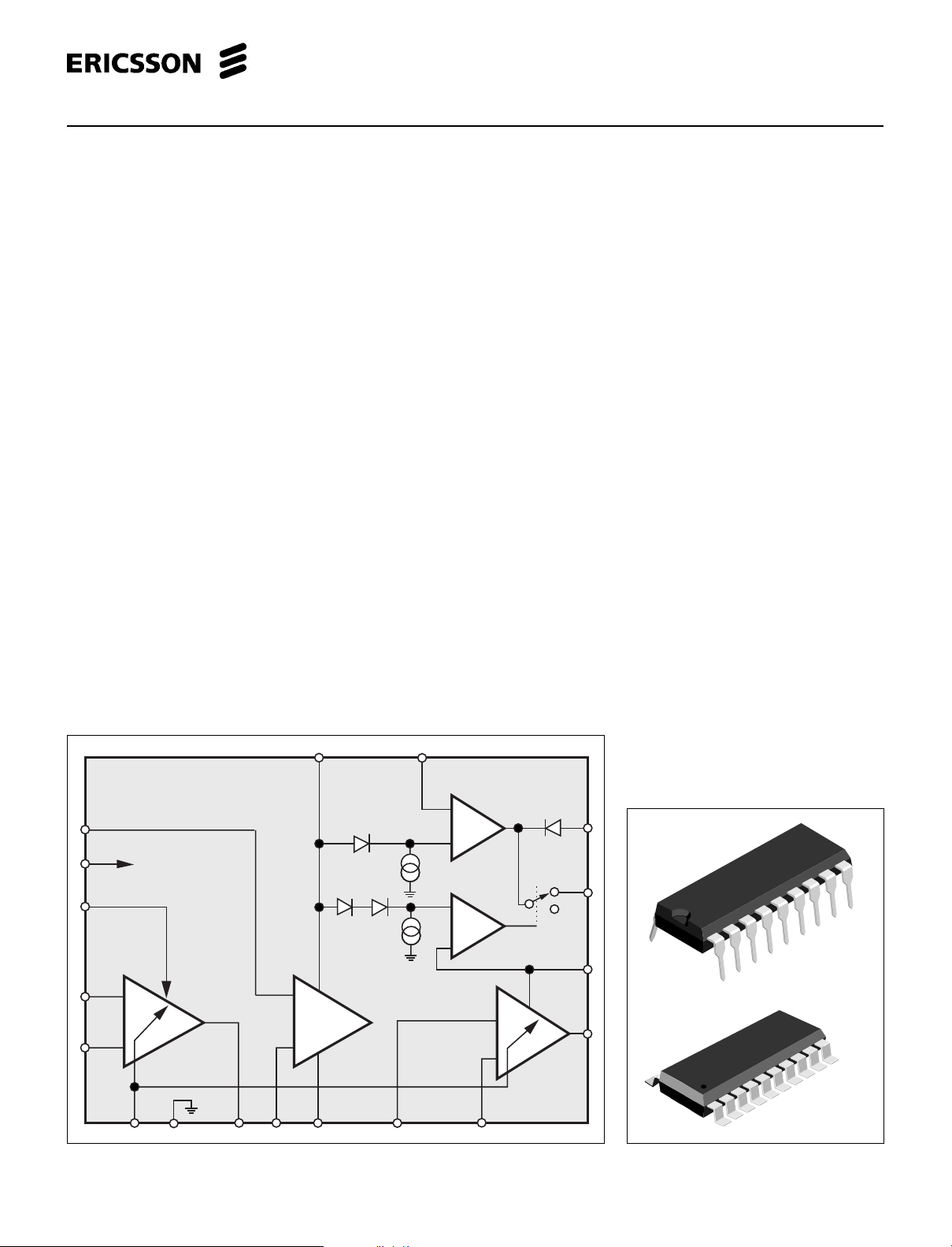
Key Features
• Low own current consumption
• Can operate both with active and
passive impedance towards the line
• Derives a high current from the line
for auxiliary functions, 12 mA at
16 mA line current
• Separate mute inputs for transmitter
and receiver (receiver cut off)
• Line length regulation possible (line
loss compensation
• Comes in 18 pin DIP and 20-pin SO
package
• High line current operation, max.
130mA
• Especially suitable for payphone
applications
• DTMF - confidence tone input
• Excellent RFI performance
PBL3853
-
12
MA
Rx
13
6
14
Figure 1. Block diagram. Pin numbers in all figures refer to DIP package.
11
2
3
17
Tx
15
18
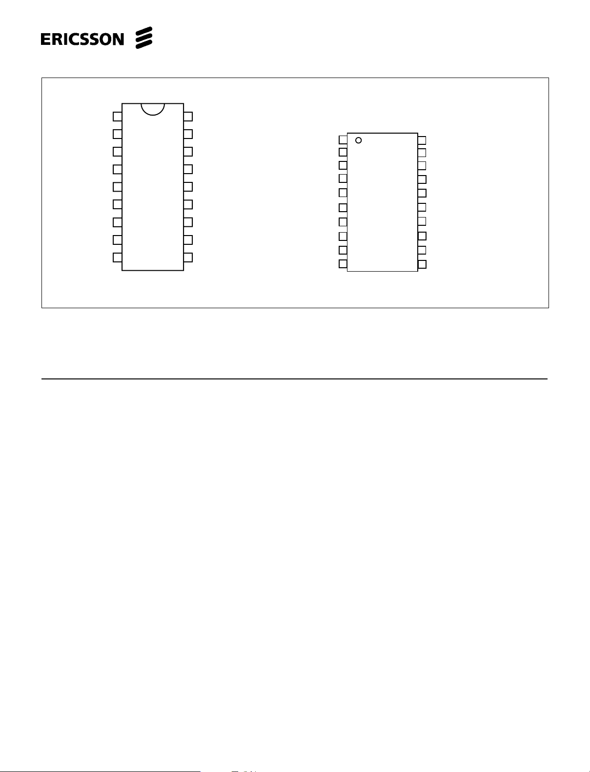
18-pin plastic DIP
16
PBL3853
20-pin plastic SO
PBL 3853
R -0-4kΩ
L
0 ohm when artificial
line is used
R = 400Ω+400Ω
feed
+
E= 50V
C = 1µF when artificial line is used
470µF when not used
5H+5H
V
I
L
+ LINE
MIC
I
DC
V
DC
Recelver
cut-off
Transmitter
mute
PBL 3853
see fig 4
-
LINE
Recevler
tone
input
REC
V
4
ARTIFICIAL
+
LINE
C
600Ω
V
2
1
V
L
Z
Rec
Z =150Ω
Mic
V
3
Z= 500Ω
V
5
=350Ω
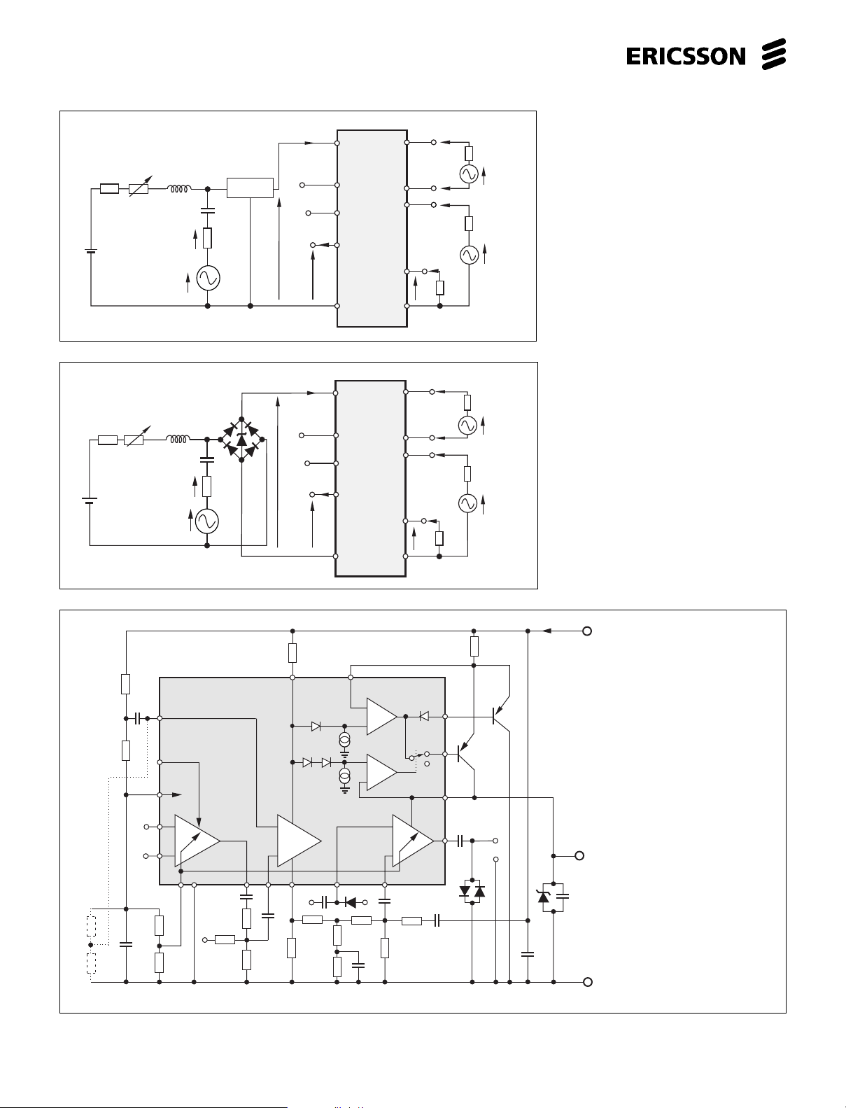
Figure 2. Test set up without rectifier
bridge.
0 ohm when artificial
line is used
R = 400Ω+400Ω
feed
+
E= 50V
R1
R2
R
A
R
B
R -0-4kΩ
L
C1
Mic
+
C3
U = 15-16V
5H+5H
1µF
600Ω
V
2
V
1
PBL3853
5
AC-DC char. adjust
Transmitter mute
10
4
+
V
12
M
13
6
14
C
R
R
D
DTMF
In
R
DTMF
I
z
L
+ LINE
MIC
Recelver
cut-off
Transmitter
mute
PBL 3853
see fig 4
-
LINE
Recevler
tone
input
REC
V
Z
4
Rec
I
DC
V
L
V
DC
Z =150
Mic
V
3
Z= 500Ω
V
5
Ω
350
Ω
Figure 3. Test set up with rectifier bridge.
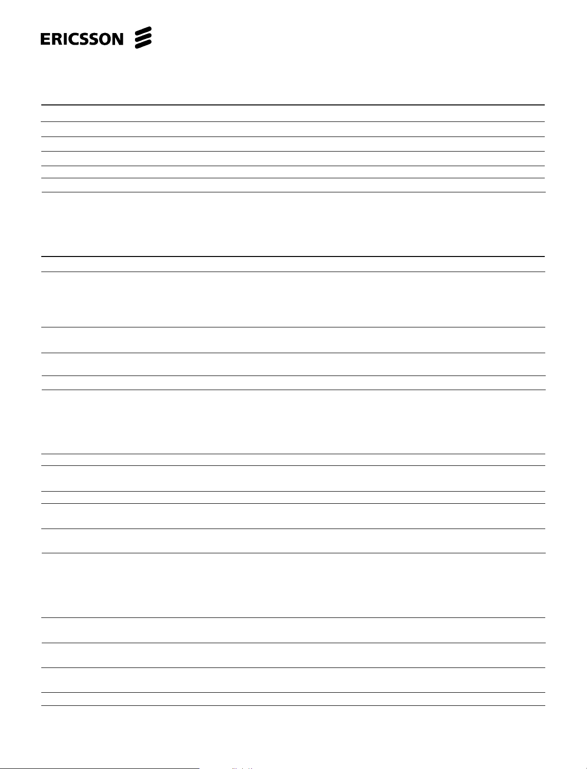
I
+ Line
R12
1
9
-
+
+
-
7
8
+
-
18
R 13
T2
T1
L
R1 = 2.7 k C1 = 150 nF
R2 = 22 Ω C2 = 10 nF
R3 = 6.8 k C3 = 47 µF
R4 = 1.8 k C4 = 220 nF
R5 = 75Ω C5 = 150 nF
R6 = 910 Ω C6 = 47 nF
R7 = 6.2k C7 = 100 nF
R8 = 560Ω C8 = 68 nF
R9 = 11 k C9 = 4.7µF
C9
16
Cut-off
R7
C6
15
R
x
Receiver
C7
R11
R10
+
Rec
D3
D2
C8
D1
C2
T
X
11
3
C4
C5
R3
R4
R5
2
Tone in
R6
17
R8
R9
R10 = 4.7k C10 = 22 µF
R11 = 120k
V
DC
R12 = 56Ω D1 = Z 4.5 V
R13 = 68Ω D2 = 1N4148
+
-Line
= 30 k* D3 = 1N4148
R
C
C10
R
= 11k*
D
* values for the test set up only
T1 = BC178B
T2 = BC178B
Figure 4. Reference figure with line length regulation. DIP-package.
2
PBL 3853
Absolute Maximum Ratings
Parameter Symbol Conditions Min. Max. Unit
Line voltage V
Continous operating line current, T
Continous operating line current, T
=70°CI
amb
=70°CI
amb
Input voltage, all inputs V
Operation temperature T
Storage temperature T
L
L
L
pinx
amb
sto
Dual In Line package 130 mA
Small Outline package 100 mA
-0.5 Vpin4+0.5 V
-20 +70 °C
-55 +125 °C
Electrical Characteristics
T
=+25°C. No cable and or line rectifier unless otherwise specified.
amb
Parameter Symbol fig. Conditions Min. Typ. Max. Unit
Terminal voltage 2 IL = 20 mA 6 V
Transmitter gain 2 20 •
Transmitter gain temp
dependence 2 I
Transmitter attenuation in
mute mode 2 60 dB
Transmitter frequencey response 2 200 Hz - 3.4 kHz -1 +1 dB
Receiver gain 2 20 •
Receiver gain temp dependence 2 IL = 20 mA, 0 - 50°C-1 +1dB
Receiver tone gain 2 20 •
Receiver frequency response 2 200 Hz - 3.4 kHz -1 +1 dB
Microphone input impedance 2 1 kHz 1.3 1.7 2.1 kΩ
(Differential)
Transmitter input impedance
Pin 3 4 1 kHz 13 17 21 kΩ
Transmitter dynamic output
voltage 2 200 Hz - 3.4 kHz < 10% distortion
Transmitter Max. output voltage 2 200 Hz - 3.4 kHz, V
Receiver input impedance
Pin 15 4 1 kHz 28 35 42 kΩ
Receiver tone input impedance
Pin 17 2 1 kHz, Not mute. Note 1 7.0 8.8 11 kΩ
Receiver output impedance 2 1 kHz 6 Ω
Ref
10
log (V2/ V3),1 kHz
I
= 57 mA 41.6 43.0 44.4 dB
L
= 0 Ω 41.0 43.0 45.0 dB
R
L
= 900 Ω - 2.2 kΩ 46.0 48.0 50.0 dB
R
L
I
= 20 mA 47.0 48.0 49.0 dB
L
= 20 mA, 0-50°C-1 +1dB
L
10
log(V4/ V1),1 kHz
IL = 57 mA -17.9 -16.5 -15.1 dB
RL = 0 Ω -18.5 -16.5 -14.5 dB
R
= 900 Ω - 2.2 kΩ -13.5 -11.5 -9.5 dB
L
IL = 20 mA -12.5 -11.5 -10.5 dB
10
log (V4/ V5), 1 kHz
IL = 25 mA 4.5 6 7.5 dB
I
= 20 mA - 100 mA 1.8 Vp
L
IL = 16mA, V
= 4.5V , IDC = 12mA 1.4 Vp
DC
IL = 16mA, VDC = 4.0V, IDC = 10mA 1.8 Vp
= 0 - 1Vrms
3
IL = 0 mA - 100 mA 3 Vp
22 V
3
PBL 3853
Parameter Symbol fig. Conditions Min. Typ. Max. Unit
Ref
Receiver dynamic output
voltage 2 200 Hz - 3.4 kHz< 2% distortion
I
= 20 mA - 100 mA 0.6 Vp
L
Zrec = 150 Ω 0.25 Vp
Receiver Max. output voltage 3 Measured with rectifier
200 Hz - 3.4 kHz
I
= 0 mA - 100 mA
L
V
= 0 -50 Vrms 0.8 Vp
1
Transmitter output noise 2 Psoph - weighted rel. 1 V
RL = 900 Ω -74 dB
Receiver output noise 2 Psoph - weighted rel. 1 V, with cable: -80 dB
0 - 5 km, Ø = 0.5 mm
0 - 3 km, Ø = 0.4 mm
Mute input voltage at mute
(transmit) V
M
22V
Input voltage at cut off
(receive) V
M
2 Note1 3 V
DC-supply current 2 IL = 16 mA, VDC = 4.5 V 12 mA
Note: 1. This input has three functions (see page 7). No input should be set on higher level than +V.
Psoph
Psoph
4
+L
PBL 3853
1
18
VDC
TO
2
TI
3
+C
4
DCAC
5
GR
6
T2
7
T1
8
FE TM
9 10
17
16
15
14
13
12
11
RI 2
RO
RI 1
-L
MI 2
MI 1
MO
+L
TO
+C
DCAC
GR
T2
NC
1
2
3
TI
4
5
6
7
T1
8
912
FE
10
20
VDC
RI2
19
RO
18
RI1
17
-L
16
MI 2
15
14
MI 1
MO
13
TM
11
NC
18 pin-DIP 20 pin-SO
Figure 5. Pin configuration.
Pin Description
DIP SO Symbol
1 1 +L Output of the transmitter (+Line side)
2 2 TO Output of the transmitter (side tone signal)
3 3 TI Input of the transmitter amplifier
4 4 +C The circuit supply (sinks ~ 0,3 mA)
5 5 DCAC Adjustment for DC-char. and AC imp. to line
6 6 GR Gain regulation starting point setting
7 7 T2 Output for transistor 2, active when voltage on the line is too low for VDC
8 8 T1 Output for transistor 1, active when charging current into VDC’s reservoir capacitor
9 9 FE Feedback
10 NC No connection
11 NC No connection
10 12 TM Transmitter mute input
11 13 MO Microphone amplifier output
12 14 MI
13 15 MI
14 16 -L Negative terminal of the circuit
15 17 RI1 Receiver amplifier input (gain control)
16 18 RO Receiver amplifier output
17 19 RI 2 Receiver amplifier input for cut-off, see page 7.
18 20 VDC VDC supply terminal
1 Microphone amplifier inverting input
2 Microphone amplifier non inverting input
5
 Loading...