


Maintenance Manual
LPE-200
SCAN And SYSTEM
PORTABLE RADIOS
900 MHz
ericssonz

AE/LZB 119 1902 R1A
MANUAL REVISION HISTORY
REVISION |
DATE |
REASON FOR CHANGE |
R1A |
DEC 1996 |
Original issue |
|
|
|
NOTICE!
This manual covers Ericsson and General Electric products manufactured and sold by Ericsson Inc.
NOTICE!
Repairs to this equipment should be made only by an authorized service technician or facility designated by the supplier. Any repairs, alterations or substitution of recommended parts made by the user to this equipment not approved by the manufacturer could void the user’s authority to operate the equipment in addition to the manufacturer’s warranty.
NOTICE!
The software contained in this device is copyrighted by Ericsson Inc. Unpublished rights are reserved under the copyright laws of the United States.
This manual is published by Ericsson Inc., without any warranty. Improvements and changes to this manual necessitated by typographical errors, inaccuracies of current information, or improvements to programs and/or equipment, may be made by Ericsson Inc., at any time and without notice. Such changes will be incorporated into new editions of this manual. No part of this manual may be reproduced or transmitted in any form or by any means, electronic or mechanical, including photocopying and recording, for any purpose, without the express written permission of Ericsson Inc.
Copyright© December 1996, Ericsson Inc.
2

|
AE/LZB 119 1902 R1A |
TABLE OF CONTENTS |
|
SPECIFICATIONS...................................................................................................................................................................... |
4 |
GENERAL............................................................................................................................................................................... |
4 |
RECEIVE ................................................................................................................................................................................ |
5 |
TRANSMIT............................................................................................................................................................................. |
5 |
DESCRIPTION ........................................................................................................................................................................... |
6 |
MECHANICAL ....................................................................................................................................................................... |
7 |
OPTIONS AND ACCESSORIES ............................................................................................................................................... |
7 |
OPERATION............................................................................................................................................................................... |
8 |
CONTROLS ............................................................................................................................................................................ |
8 |
KEYPAD SCAN/SYSTEM FUNCTIONS.............................................................................................................................. |
9 |
CIRCUIT ANALYSIS............................................................................................................................................................... |
10 |
SOFTWARE.......................................................................................................................................................................... |
10 |
RECEIVER............................................................................................................................................................................ |
10 |
RX Front End..................................................................................................................................................................... |
10 |
Rx Back End ...................................................................................................................................................................... |
11 |
TRANSMITTER ................................................................................................................................................................... |
13 |
Transmit Frequency Generation......................................................................................................................................... |
13 |
TX/Converter/Modulator (N150)....................................................................................................................................... |
13 |
SAW Transmit Band Pass Filter 1 ..................................................................................................................................... |
14 |
MMIC Buffer Amplifier .................................................................................................................................................... |
14 |
SAW Transmit Band Pass Filter 2 ..................................................................................................................................... |
14 |
Power Amplifier (N101) .................................................................................................................................................... |
14 |
Directional Coupler (W100) .............................................................................................................................................. |
14 |
Power Sensor Circuit (N102-A)......................................................................................................................................... |
14 |
Power Control Buffer (N102-B) ........................................................................................................................................ |
15 |
Transmit Low-Pass Filter/Antenna Switch......................................................................................................................... |
15 |
Transmit Modulation ......................................................................................................................................................... |
15 |
SYNTHESIZER..................................................................................................................................................................... |
15 |
Dual Synthesizers (N203) .................................................................................................................................................. |
15 |
Bilateral Switch (N201) ..................................................................................................................................................... |
15 |
Main Voltage Controlled Oscillator (U200) ...................................................................................................................... |
15 |
Main Synthesizer (N203) ................................................................................................................................................... |
16 |
Auxiliary Synthesizer (N203) ............................................................................................................................................ |
16 |
Reference Oscillator (U201) .............................................................................................................................................. |
16 |
DC POWER DISTRIBUTION .............................................................................................................................................. |
16 |
Synthesizer Regulator (N290)............................................................................................................................................ |
16 |
Receiver Regulator (N490) ................................................................................................................................................ |
16 |
Transmit Regulator (N190)................................................................................................................................................ |
16 |
Tx Switch (V192) .............................................................................................................................................................. |
17 |
B+ Switch (V191).............................................................................................................................................................. |
17 |
Analog Regulator (N900) .................................................................................................................................................. |
17 |
+5V-D Switching Regulator (N902) .................................................................................................................................. |
17 |
LCD NEGATIVE BIAS GENERATOR ............................................................................................................................... |
18 |
SERVICE................................................................................................................................................................................... |
18 |
EQUIPMENT REQUIRED ................................................................................................................................................... |
18 |
PROGRAMMING ................................................................................................................................................................. |
18 |
Personality Programming................................................................................................................................................... |
18 |
Flash Programming ............................................................................................................................................................ |
19 |
Programming Mode ........................................................................................................................................................... |
19 |
3

AE/LZB 119 1902 R1A
BASIC TROUBLESHOOTING ............................................................................................................................................ |
19 |
ERROR CODES INTRODUCTION ..................................................................................................................................... |
22 |
ERROR CODE OVERVIEW ................................................................................................................................................ |
22 |
Error Code Format ............................................................................................................................................................. |
22 |
Fatal Errors ........................................................................................................................................................................ |
22 |
Non-Fatal Errors ................................................................................................................................................................ |
23 |
Special Error Codes ........................................................................................................................................................... |
23 |
ERROR CODES - SPECIFIC................................................................................................................................................ |
23 |
Hardware Fatal System Errors ........................................................................................................................................... |
23 |
Operational Software Fatal System Errors ......................................................................................................................... |
24 |
Operational Software Non-Fatal System Errors................................................................................................................. |
25 |
Radio Programming Errors ................................................................................................................................................ |
26 |
DISASSEMBLY PROCEDURE ............................................................................................................................................... |
28 |
PA Module Replacement ................................................................................................................................................... |
30 |
Filters Z400 And Z401 Replacement ................................................................................................................................. |
30 |
REASSEMBLY ..................................................................................................................................................................... |
30 |
|
SPECIFICATIONS* |
|
GENERAL |
|
|
FCC Identification Number |
AXATR-357-A2 |
|
DOC Certification Number |
|
|
Input Voltage |
7.5 Vdc (nominal) |
|
Frequency Range: |
|
|
Transmit |
* 896 - 901 MHz |
935 - 940 MHz |
Receive |
935 - 940 MHz |
|
Frequency Stability |
±1.5 PPM |
|
Dimensions (Typical)H x W x D: |
|
|
Less knobs and antenna |
|
|
with High Capacity Battery |
144 mm x 67 mm x 43 mm |
|
with Extra High Capacity Battery |
157 mm x 67 mm x 43 mm |
|
Weight: |
|
|
with High Capacity Battery |
20.8 oz. (589 g) |
|
with Extra High Capacity Battery |
22.0 oz. (624g) |
|
Operable Temperature Range |
-30°C to +60°C (-22°F to +140°F) |
|
Continued
4

AE/LZB 119 1902 R1A
|
SPECIFICATIONS (Con't) |
RECEIVE |
|
Channel Spacing |
12.5 kHz |
Sensitivity (12 dB SINAD) |
-118dBm |
Selectivity: |
-63 dB |
Intermodulation |
-67 dB |
Frequency Separation |
Full Bandwidth |
Audio Output |
500 mW @ 3% Maximum Distortion |
TRANSMIT |
|
RF Power Output |
0.5 - 3 Watts (Normal Trunked) |
Spurious and Harmonics |
-55 dBc |
Modulation/Deviation |
±2.5 kHz |
Frequency Separation |
Full Bandwidth |
FM Hum & Noise |
-35 dB |
(Companion Receiver) |
|
Audio Distortion |
Less than 3% @ 1000 Hz, 3 kHz deviation |
Frequency Stability |
±1.5 PPM |
(-30°C to +60°C: + 25 Ref) |
|
Audio Frequency Response |
EIA |
These specifications are intended primarily for the use of the service technician. See the appropriate Specification Sheet for the complete specifications.
5

AE/LZB 119 1902 R1A
DESCRIPTION
The Ericsson Inc. LPE-200 Portable Radios are rugged, high-quality, high-performance FM two-way communications unit. It is available in either Scan or System versions. These are Ericsson’s smallest and most sophisticated high-specification portable radios, designed to meet worldwide requirements. They utilize custom designed integrated circuits to set new standards for size and weight for a high power, high specification two way radio. These radios are synthesized and can be programmed to operate on both EDACSâ trunked or conventional communications systems. Features include:
∙Compact Size
Designed small and light with rounded edges to fit comfortably in your hand, while providing specifications and performance superior to larger, heavier radios.
∙Light Weight, Rugged Constructions
Features a molded case made of a polycarbonate blend surrounding a metal casting. This construction provides a lightweight yet durable housing designed to withstand years of rugged use.
∙High System/Group Capacity
Both the Scan and the System versions can manage up to 800 different EDACS system/group combinations with up to 200 conventional channels. EDACS systems/groups can be configured in many different ways to meet specific user needs.
∙Dual Mode Capability
Conventional operation by simply selecting a preprogrammed conventional system.
∙Transmit Indicator
A red LED indicator on the top of the radio indicates when the radio is transmitting.
∙Display
System and group information, status icons and menu operation is supported by the 3-line, 12-character, alphanumeric back lit Liquid Crystal Display (LCD).
∙Top-Mounted Rotary Knobs
The rugged rotary knobs are designed for ease of operation by allowing tactile access to groups, systems, conventional channels, as well as volume and power control. Knobs are designed with metal protective sleeves which help prevent bent and broken knobs due to impact.
∙Keypad
The back lit keypad allows the user to access the many radio functions. The 6-button SCAN provides easy access to preprogrammed telephone and individual radio ID’s, while the 15-button System keypad expands this capability, allowing direct entry of these numbers. The LPE-200 radios have a keypad with translucent keys. A detailed description of the keypads and their additional function is found in the OPERATION section.
∙Emergency ID And Alarm
The user can alert the dispatcher to an emergency by pressing a recessed red button located on the top of the radio which sends user ID and an emergency signal.
∙Universal Device Connector (UDC)
The UDC provides the PC programmer and optional accessories access to the radio for ease and versatility of radio functionality.
∙Variable Power Control
PC Programmable from 0.5 to 3 watts
∙Weatherproof
Radios operate reliably under adverse conditions. These portable radios meet military standards MIL810C, D and E specifications for temperature and pressure extremes, solar radiation, driven rain, humidity, salt fog, blowing dust, shock and vibration.
∙Vibration
Meets EIA, U.S. Forest Service and MIL-810 environmental and vibration-stability requirements.
∙Personality Programming
Can easily be hooked up to a personal computer in the field, to allow system and radio parameters to be flexibly programmed as requirements change, without changing parts or opening the radio case.
6
AE/LZB 119 1902 R1A
MECHANICAL
The radios are packaged in a polycarbonate blend exterior housing. A six-cell back mounted nickel cadmium battery pack provides a nominal 7.5 volts. Two different nickel cadmium battery packs offering high and extended capacities are available for use with the portable radios.
The top of the radio has a Volume, Channel/ Area/System select knob, Emergency/Home button, TX LED and a screw-on antenna mount connector. Located on the front is a 3-line 12 character per line dot matrix LCD with backlighting. A chip-on-glass filtered super twisted nematic LCD with a transflective rear film is used. A 36 mm speaker and electret microphone are located above the LCD. Below the speaker is either a 6-button keypad for Scan operation or a 15-button keypad for System operation. A push-to-talk bar is located on the left side along with a Clear/Monitor button and option button. On the opposite side a UDC connector is located for plug-in accessories and PC programming.
One printed wire board assembly contains the transmitter/receiver, audio and logic circuitry. A separate printed wire board assembly (daughter board) contains the DSP Module. The radio board assembly is cradled in a zinc die casting which is used as a PA heat sink and for housing rigidity. A sheet metal shield completes the RF shielding.
The keypad and LCD assembly are separate from the main board and interconnect by a flex-circuit. This flexcircuit also interconnects the speaker, microphone and UDC assemblies. Top controls mount to another flex-circuit board that plugs into the main radio board assembly.
Radio circuitry is centered mainly on one radio board. This board is mounted in a metal housing with a metal shield covering the top of the board. This enclosure is penetrated only by a flex cable which ties the front, user interface part of the radio to the board and a 3-pin battery connector. Surface mount components populate both top and bottom of the radio board allowing a combination of both RF and digital circuits. Only a few leaded parts are used where no surface mount components are available.
OPTIONS AND ACCESSORIES
PART NUMBER |
DESCRIPTION |
|
|
Batteries
BKB 191 203 High Capacity NICAD Battery
BKB 191 202 Extra High Capacity NICAD Battery
BKB 191 203/A2 High Capacity NICAD Battery (FM
Intrinsically Safe)
BKB 191 202/A2 Extra High Capacity NICAD Battery (FM Intrinsically Safe)
Chargers
BML 161 51/505 120 Volt, Rapid (Ericsson label)
BML 161 51/506 120 Volt, Rapid (GE label)
BML 161 51/507 230 Volt, Rapid (Ericsson label)
BML 161 51/513 120 Volt, Multi Rapid (Ericsson label)
BML 161 51/514 120 Volt, Multi Rapid (GE label)
BML 161 51/515 230 Volt, Multi Rapid (Ericsson label)
Antenna
KRE 101 1223/02 900 MHz Whip Antenna
Carrying Accessories
KRY101 1605/01 Leather Case With Belt Loop
KRY101 1605/A2 Leather Case W/Swivel And Belt Loop
KRY 101 1609/A1 Belt Loop With Swivel
KRY 101 1232/2 Plastic Belt Clip
KRY 101 1607/1 Leather Shoulder Strap
Audio Accessories
KRY 101 1617/1 Speaker Microphone (GE label)
KRY 101 1617/3 Speaker Microphone (Ericsson label) KRY 101 1617/A2 Speaker Mic., With Antenna (GE label)
KRY 101 1617/A4 Speaker Mic., With Antenna (Ericsson
label)
RLD 541 07/11 Earpiece Kit, Speaker Microphone
7

AE/LZB 119 1902 R1A
OPERATION
The LPE-200 series of portable radios is designed for EDACS and conventional mode operation. When the unit is used in a trunked EDACS, the digital control channel is automatically monitored. When the user initiates a call, the unit sends a digital request through a control channel to the site controller. The site controller then assigns the calling radio and all members of the talk group to an available working channel. All operations in EDACS configurations are supported from a single-site system to wide-area trunking networks.
For more detailed operating instructions refer to Operator’s Manual AE/LZT 123 1868.
CONTROLS
The radio features two rotary control knobs and an emergency button mounted on the top of the radio, with side-mounted push-to-talk, monitor/clear and option buttons. The front-mounted keypad has 6 buttons on the Scan and 15 buttons on the System (refer to Figure 1).
∙Power/Volume Knob
This knob controls power to the radio (On/Off) and adjusts the Volume level of the speaker.
∙Control Knob
A 16-position rotary switch can select systems, groups or conventional channels. The knob is fitted with a variable hardware stop for radio customization.
∙Emergency Button
A recessed red button on the top of the radio initiates an emergency alert to the dispatcher and talk group members.
∙PTT Button
The weather-sealed Push-To-Talk (PTT) button must be pressed before voice transmission begins. Pressing the PTT button transmits the unit ID. In trunked mode, the ID is transmitted upon depression of the PTT button.
∙Clear/Monitor Button
In the trunked mode, the weather-sealed Clear/Monitor button is used:
1)to exit the current operation, removing all displays associated with it and return the radio to the selected talk group.
2)to hang-up individual and telephone interconnect calls.
In the conventional mode, the Clear/Monitor button functions are:
1)to unsquelch the receiver to allow channel monitoring prior to transmission.
2)to remove Channel Guard Decoding from a channel.
∙Option Button
The weather-sealed option button activates one of a number of programmable software options selected during PC programming. Programmable options include high/low power setting, keypad lock, LCD contrast, LCD and keypad back lighting.
System/Group/
Power On/Off Channel Knob
Volume Knob
|
Antenna |
|
TX LED |
Emergency |
|
Button |
||
|
Battery Release
Button
Option Button
Clear/Monitor
Button
Push-To-Talk
(PTT) Button
Figure 1 - Controls (Top, Back and Left Panel Views)
8

AE/LZB 119 1902 R1A
KEYPAD SCAN/SYSTEM FUNCTIONS
Figure 2 - Scan Keypad
|
|
Figure 3 - System Keypad |
|
|
|
|
Key |
Function |
|
|
|
|
▲ ▼ |
Primary Function: Allows user to select |
|
either system, groups, or channels, depending |
|
|
|
|
|
|
on personality programming. The buttons act |
|
|
as STEP UP or STEP DOWN. Pressing one |
|
|
of these buttons displays the next or previous |
|
|
stored system, group or channel. |
|
|
Secondary Function: Changes the selection |
|
|
for an item within a list. |
|
|
|
MPrimary Function: Accesses the pre-stored menu. The menu can include high/low power setting, keypad lock, LCD contrast, LCD and keypad back lighting.
Secondary Function: Activates a selected item within a list. After a menu list is accessed, scroll through the list using the  ,
,  keys and then activate specific items with the M key. This is similar to an “Enter” key.
Key |
|
Function |
|
|
|
||
A/D |
Adds/Deletes selected groups or channels |
||
(Scan |
from the Scan list of the currently selected |
||
only) |
system. |
|
|
|
|
||
SCN |
Turns the Scan operation On and Off. |
||
(Scan |
|
|
|
only) |
|
|
|
OPT |
Activates one of a number of programmable |
||
(Scan |
software options, selected during the PC |
||
only) |
programming. |
Programmable options |
|
|
include high/low transmitter power and talk- |
||
|
around. |
|
|
|
|
||
1 |
Used to select a specific system. If the rotary |
||
(System |
knob is used to select the system and more |
||
than 16 systems are programmed in the radio, |
|||
only) |
|||
the key is used to select additional |
|||
|
|||
|
banks (groupings) of systems. |
||
|
|
||
1-9, *, |
These keys are used to place telephone |
||
0, # |
interconnect and individual (unit-to-unit) |
||
(System |
calls. The keys operate like a normal |
||
telephone keypad. |
|||
only) |
|
|
|
|
|
||
2 |
Used to select a specific group. |
||
(System |
|
|
|
only) |
|
|
|
|
|
||
3 |
Used to turn the SCAN operation on and off. |
||
(System |
|
|
|
only) |
|
|
|
|
|
||
* |
Used to place telephone interconnect calls. |
||
(System |
|
|
|
only) |
|
|
|
|
|
||
# |
Used to initiate individual calls. |
||
(System |
|
|
|
only) |
|
|
|
|
|
||
6 |
Adds groups or channels from the Scan list of |
||
(System |
the currently selected system. |
||
only) |
|
|
|
|
|
||
9 |
Deletes selected groups or channels from |
||
(System |
Scan list of the currently selected system. |
||
|
|
||
only) |
|
|
|
|
|
|
|
9

AE/LZB 119 1902 R1A
CIRCUIT ANALYSIS
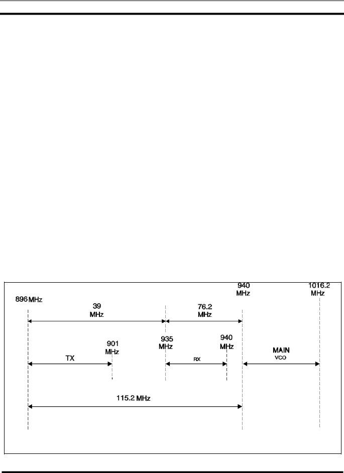
The portable radio is unique in the generation of the transmit carrier. The transmit section has an offset frequency loop operating at 115.2 MHz. This means the synthesizer is operating at a frequency that is not harmonically related to the output frequency.
The radio contains five custom integrated circuits as follows:
∙DEBBIE (D601) - Has three major functions: digitizing, voice CODEC and digital to analog conversions.
∙HILLARY (D701) - Contains the microprocessor, phase digitizer, frequency discriminator and sigma/delta modulator to provide digital modulation.
∙JACQUI (N150) - Generates the transmit carrier frequency from the main VCO frequency. Generates the transmit offset oscillator frequency and provides modulation through the I/Q inputs.
∙CHERYL ( N203) - The main and auxiliary frequency synthesizers for the main VCO and the 2nd Local Oscillator (LO).
∙DIANE (N551) - Contains the 2nd mixer and the LO for the 2nd mixer. Contains a limiter circuit which provides a balanced output to HILLARY. Provides the receiver 2nd IF and the Receiver Signal Strength Indicator (RSSI) signal.
The Schematic Diagram for this unit consist of 16 sheets. Component coordinates are provided so the technician can locate different points with ease. For example: A point may be labeled 7-B16. This means that this point connects to a point shown on sheet 7 with coordinates B (read up) and 16 (read right). Borders with vertical and horizontal coordinates are provided to facilitate this capability.
SOFTWARE
Software in the microprocessor handles basic radio controls, interfaces and system protocols. The HILLARY chip and DSP handles all modulation, demodulation and speech processing functions.
Microprocessor software consists of:
∙RAM Bootloader Software - downloaded by the PC programmer into the radio and executed. This software communicates with the PC using a full network protocol (x3.28). Serial data is transferred through the radio UART for FLASH application loading, DSP code
storage and personality storage. This software supports read/write of EEPROM data such as Tracking Data and Feature Encryption. Data compression is used to reduce FLASH application loading time.
∙FLASH Application Software - the main radio controller software. It is divided into the platform and application modules. The platform software provides the hardware level interface, operating system, run-time libraries and software standby (sleep) operation. The application software provides all of the user interface trunked signaling, conventional signaling, diagnostics, debugging capability, UDC device support and personality interface.
DSP software includes:
∙FM Audio Processing - Transmit
∙FM Audio Processing - Receive
∙Transmit Waveform Generation
∙Transmit Waveform Combinations
∙Demodulation/Decoding
∙Demodulation/Decoding Combinations
RECEIVER
RX Front End
The 935-940 MHz RF receive frequency is passed from the antenna through a low pass filter/antenna switch to the input of fixed ceramic band pass filter Z400 (Pin 1). The band pass center frequency is 938 MHz and the gain through the filter is typically -1.5 dB. The output of Z400 (Pin 2) is coupled through capacitor C400 and impedance matching inductor L400 to the base of RF amplifier transistor V400.
RF Amplifier (V400)
RF amplifier transistor V400 provides typically +16 dB of gain to the RF signal. The gain of this stage is controlled by feedback voltage from IF AMP 1 transistor V500 which sets the bias of V400. The emitter voltage of V500 is connected to the collector of V400 through resistors R504 and R401, and filter capacitors C506 and C507. This voltage can be metered at TP400. The bias to the base of V400 is set by resistor R400. RF coil L401 tunes the amplifier load. The output of V400 is coupled through fixed ceramic band pass filter Z401 (Pin 1). The band pass center frequency is 938 MHz and the gain through the filter is typically -1.5 dB. The output of Z401 (Pin 2) is connected to the input of mixer circuit Z402 (Pin 5).
10
AE/LZB 119 1902 R1A
Local Oscillator Buffer (V450)
The injection frequency (1011.2-1016.2 MHz) from the synthesizer circuit is applied to the base of Local Oscillator (LO) NPN buffer transistor V450 through capacitor C450 and inductor L450. This signal at the input of V450 is 0 dBM and is amplified to +4 dBm. This signal can be metered at TP450. The output of V450 is connected to the input of mixer Z402 (Pin 1).
Mixer (Z402)
The LO frequency and the RF signal are mixed to provide an Intermediate Frequency of 76.2 MHz (example: 1011.2 MHz - 935.851 MHz = 76.2 MHz). This signal on the output of Z450 (Pin 4) is applied to the base of IF AMP 1 NPN transistor V500 through filter capacitor C505, inductor L500 and coupling capacitor C504.
IF Amp 1 (V500)
IF AMP 1 amplifies the 76.2 IF signal +15 dB. The collector voltage for V500 is from the emitter of LO BUFFER amplifier V450 and can be metered at TP500 (3.8 V). The emitter voltage of V500 is used as feed back to control the gain of RF amplifier V400. The output from the collector of V500 is connected through coupling capacitor C502 to the input of band pass Filter Z500 (Pin 4).
IF Filter (Z500)
IF band pass Filter Z500 is a 4-pole crystal filter. The gain of Z500 is -3 dB and the center frequency is 76.2 MHz. The output of Z500 (Pin 6) is coupled to the emitter circuit of IF AMP 2 through a limiting zener diode circuit consisting of zener diodes V502-1 and V502-2 and coupling capacitor C508.
IF Amp 2 (V501)
The typical emitter voltage of V501 is 0.8 V. The typical base voltage is 1.6V and the typical collector voltage is 3.1 V. These voltage levels produce the proper bias for an input impedance of 250 ohms. This in turn loads the Z500 crystal filter properly. The 76.2 MHz IF output on the collector of V501 connects to the input of a 450 kHz IF chip (N551) located in the rear section of the LPE-200.
Rx Back End
IF Chip (N551)
The IF input (76.2 MHz) to IF Chip N551 is connected through coupling capacitor C550 and inductor L550 to N551 Pin 1, (RF+). Internal to N551 (DIANE), this input signal is amplified and applied to an input of a second mixer circuit. A second LO synthesizer injection frequency
of 76.2 MHz is internally applied to another input of the mixer circuit. This results in a second IF of 450 kHz (76.65 MHz -76.2 MHz = 450 kHz) on the output of the mixer (N551, Pin 20, Mixer Out). This signal is then routed through a 450 kHz ceramic filter to set the channel bandwidth to 12.5 kHz. The output of the filter is routed to N551, Pin 18, IF In1. This input (-3 dB) to N551 is amplified and sent two places. The output (N551, Pin 16, IF Out 1) signal goes through capacitor C553 to the input of 450 kHz Ceramic Filter Z550, Pin 2. The output of Z550 on Pin 1 is connected through capacitor C552 to N551, Pin 14, IF In2. This input to N551 is further amplified and balanced outputs, RxIF and RxIF_B, are sent to HILLARY (D701). These two lines, one positive and the other negative, are used to cancel out any noise that might get on the line. These balance outputs are typically +3 dBm and can be metered at test points TP551 and TP552.
The Receiver Signal Strength Indicator (RSSI) circuitry internally monitors the RF signal strength. The RF level is represented by a DC voltage level proportional to signal strength. Feedback resistors R554 and R561 set the gain of the RSSI output on Pin 7. This signal becomes the FAST RSSI signal going to DEBBIE (D601). Feedback resistor R554 connects from the RSSI output on Pin 7 to Pin 8, RSSI Feedback. The RSSI signal can be metered at test point TP550.
2nd Local Oscillator
A 2nd LO circuit internal to N551 generates the 76.65 MHz injection frequency for the mixer circuit. The tank circuit for this oscillator consists of capacitors C556 through C560, variable capacitor V550 and inductor L551. This tank circuit connects to N551, Pin 3 (OSC Emitter) and Pin 4 (OSC Base). A LO_VCTRL control voltage is applied through resistor R555 to V550 to adjust the capacity of the circuit and maintain the integrity of the injection frequency. The LO_VCTRL control voltage is a DC level generated in CHERYL and filtered by resistors R225 and R226 and capacitors C217, C218 and C219. This voltage (nominally 2.6 volts) comes from auxiliary synthesizer N204 and goes to the oscillator tank circuit. A +12 dB signal is then returned to a prescaler circuit in the synthesizer. The synthesizer provides a signal to the loop filter which outputs the control voltage.
11

AE/LZB 119 1902 R1A
Digital I/O Lines
The balanced RxIF and RxIF_B (B implies “Barred” indicating that the condition is true when the line is low) lines connect through resistor and capacitor RF decoupling circuits to HILLARY D701. RxIF connects through resistors R715 and R714 and capacitor C707 to D701, Pin 8. RxIF_B connects through resistors R717 and R718 and capacitor C709 to D701, Pin 7. Both of these lines connect to a Phase Digitizer internal to D701.
Phase Digitizer (D701)
The phase digitizer demodulates the 450 kHz IF to recover the digitized receive audio. The output of the phase demodulator is connected to Rx DSP Interface (Refer to Schematic Diagram, Sheet 13). The Rx DSP Interface output of D701 connects to the DSP module through D701, Pin 69 (RXSIF_DSPDATA), Pin 73 (RXSIF_DSPCLK) and Pin 74 (RXIF_DSPSYNC). DSP interface lines connect to DSP TDR (TDM DATA RX), DSP TCKDR (TDM CLOCK RX) and DSP TRSR (TDM FRAME SYNC TX) respectively. These lines can be metered on the DSP module at test points TP8 (data), TP15 (clock) and TP14 (sync), respectively.
DSP Module
The Digital Signal Processing (DSP) Module does all the Channel Guard filtering, provides squelch, audio mute, 1.5, 3, and 4.5 dB of volume attenuation and changes the digitized audio into an analog signal. The output of the DSP module is on X21-17 (PCM_DSEAR). This output can be metered at test point TP3 on the DSP module.
Host Interface
The PCM_DSPEAR line connects to D701, Pin 64 and goes to the PCM/DSP HOST INTERFACE. The audio output of D701 is on Pin 40 (PCM_CDCEAR) and connects to D601, Pin 34 (DPCI).
DEBBIE (D601)
This signal (PCM_CDCEAR) is then put through a decoder, low pass filter, volume control circuit and an amplifier. The low pass filter, filters out an 8 kHz sample rate. The volume control provides 24 dB in 6 dB steps. The output of D601 is on Pin 22 (RXAUDIO). The signal can be metered at test point TP601. At maximum volume there should be 350 mVolts RMS (1.0VP-P) with a 1 kHz tone and 3 kHz deviation.
Operational Amplifier (N300)
This signal (RXAUD1) connects through capacitor C611 and resistor R625 to operational amplifier N300, Pin 6 (-B). Feedback for the amplifier is through resistor R627. The gain of this amplifier is changed by the RX_VOL_ATTN line (D701, Pin 116) to provide a total of 48 dB of volume control attenuation. This is accomplished by the RX_VOl_ATTN line going high, causing transistor V604-1 to conduct and connecting 10k ohms resistor R626 across 68k ohms resistor R627 to reduce the gain of N300B. The output of this amplifier is on Pin 7 (RXAUD2).
Audio Power Amplifier (N600)
This signal is attenuated through resistor R629 then coupled through coupling capacitor C613 to audio power amplifier N600A, Pin 7 (+IN). This signal is also connected through resistor R628 and coupling capacitor C612 to the Universal Device Connector (UDC_AUDIO_OUT). The audio input to N600A can be metered at test point TP602 and at maximum volume should be 250 mVP-P. The input will be 21 mV RMS (60 mVp-p) to produce 500 mWatts output into 16 ohms. Power amplifiers N600A and N600B provide differential outputs on Pin 1 (+OUT) which is
AUDIO_PA_HI and Pin 3 (+OUT) which is SPK_LO. The bridged output of these two lines provides 2.83 V RMS for 500 mWatts output into 16 ohms. The SPK_LO line connects through the flex circuit to the low side of the speaker. The AUDIO_PA_HI connects through resistor R641 to the other side of the speaker (SPKR_HI). Resistor R641 is used to attenuate the speaker audio during duplex operation. Normally MOSFET V602 is turned on, bypassing R641 to get the full volume to the speaker. V602 is controlled by a binary output line from HILLARY labelled DUPLEX_SPKR_ATTEN. When this line is at 0 volts, transistor V603 is off and the collector is high which turns on both V602 MOSFETs, by-passing R641. SPKR_HI then connects through the flex circuit to the high side of the speaker. Two series MOSFETS are used to prevent forward biasing the characteristic diodes across the MOSFETS with audio when the MOSFETS are OFF.
12
AE/LZB 119 1902 R1A
TRANSMITTER
Transmit Frequency Generation
The main VCO, in the synthesizer circuit, is programmed to generate the 1st LO receive injection frequency (1011.2 to 1016.2 MHz). This carrier frequency is mixed with a transmit offset frequency of 115.2 MHz to generate the carrier and two side band frequencies. The carrier and upper side band are suppressed and only the lower side band is transmitted. For example: the carrier frequency of 1015.2 MHz minus the offset frequency of 115.2 MHz is equal to the transmitted lower side band frequency of 900 MHz.
TX/Converter/Modulator (N150)
Transmit Offset
The LPE-200 transmit offset frequency is 115.2 Mhz. This frequency is generated by a seven-times-multiplier circuit off the reference oscillator. The output of this VCO is applied to a Phase-Lock-Loop (PLL) where it is divided by 7 (115.2 ÷ 6 = 19.2 MHz) and compared to a reference frequency of 19.2 MHz. The 19.2 MHz reference frequency is generated by oscillator module U201 in the synthesizer circuit. A DC phase lock voltage, which is the difference of the two input frequencies, on N150, Pin 9 (PHSOUT) is applied to a loop filter. This loop filter consists of capacitors C151, C152 and C155 and resistors R153 and R154. The DC voltage can be metered at test point TP150 and should be 1-4 volts while transmitting and 0 volts while
receiving. The output of the filter connects to the tank circuit through resistors R155 and R160. The tank circuit for the VCO and consists of capacitors, C160, C161, and two variable capacitors in V180 and inductor L154. The loop filter and the tank circuit are tuned to 6x19.2 MHz or 115.2 MHz. The tank circuit connects across N150, Pins 6 (TANK_1) and 7 (TANK_2). The DC voltage applied to the loop filter changes the capacitance of the variable capacitors within V180 of the tank circuit to maintain the VCO output of 115.2 MHz.
When the transmitter is keyed, transistor V152 conducts to increase the bandwidth for PLL acquisition.
Single Side Band Mixer
The main VCO frequency is amplified then passed through a 90-degrees phase shifting network to the SSB mixer. The 115.2 MHz offset frequency is also amplified and passed through a 90-degree phasing network to the SSB mixer. These two signals are summed together to produce the carrier frequency, an upper side band and a lower side band. The carrier and upper side band are suppressed by 40 dB. The lower side band passes at full amplitude. There are two outputs of the lower side band from the SSB, each 90degrees out of phase. Each signal is connected to another mixer circuit where it is summed with the transmit modulation from HILLARY. Resistor R159 sets the gain for phase detection.
Low Pass Filters
There are two modulating inputs from HILLARY, one is the I input (MODI and MODI_B) and one is the Q input
Figure 4 - Frequency Generation
13
AE/LZB 119 1902 R1A
(MODQ and MODQ_B). The I input passes through a low pass filter consisting of capacitors C191, C192 and C193, resistor R166 and inductors L156 and L157. The output of this filter connects to N150, Pins 43 (I) and 42 (I_bar). The Q input passes through a low pass filter consisting of capacitors C194, C195 and C196, resistor R167 and inductor L158 and L159. The output of this low pass filter connects to N150, Pins 41 (Q) and 40 (Q_bar). The I and Q inputs are summed with the lower side band then the outputs of these mixer circuits are summed to produce the lower side band with transmit modulation. This signal is amplified and connected through N150, Pin 34 (DUAL TX) to the input of a transmit band pass filter.
SAW Transmit Band Pass Filter 1
The TX_RF signal (0 dBm) connects through coupling capacitor C125 to the input of a TX Band Pass Filter. Filtering of the TX_RF line is provided by capacitor C126. The lower sideband output of the band pass filter (-8 dB) connects through coupling capacitors C121 and C139 to the base of buffer amplifier transistor V104. Filtering is provided by capacitor C120.
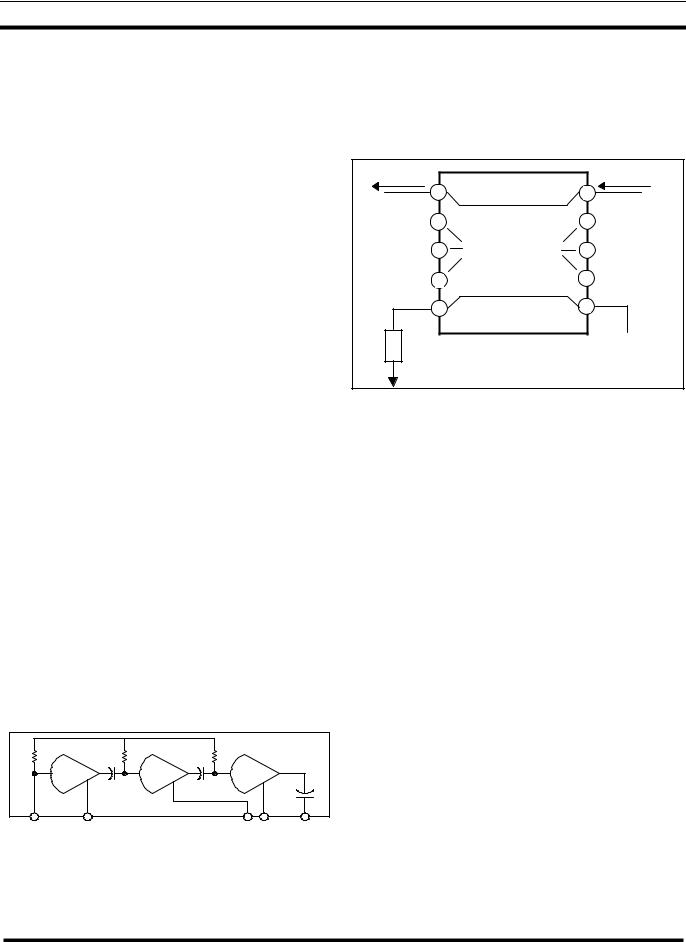
Directional Coupler (W100)
The RF output connected to W100, Pin 4 (PORT 2) connects directly through W100 to Pin 1 (PORT 1) where it is output to the antenna circuit. The connection between Pin 9 (PORT 3) and Pin 6 (PORT 4) is part of the sensing circuit (See Figure 4).
RF Output |
|
RF Input |
1 |
Port 1 |
Port 2 |
|
GND |
GND |
|
Port 3 |
Port 4 |
50 Ohms |
Power Sense |
|
|
|
Circuit N102-A |
Figure 6 - Directional Coupler
MMIC Buffer Amplifier
When transmitting, the collector voltage for transistor V104 is provided through PIN diode V101 and is controlled by DPTT. The RF output from the collector (+3 dBM) connects through coupling capacitor C116 and resistor R105 to power amplifier N101, Pin 1 (Pin/Vc).
SAW Transmit Band Pass Filter 2
The output of the MMIC Buffer amplifier is fed to the input of the second SAW BPF. This filter provides further attenuation for Tx spurions. The output of this filter is fed to the RF amplifier
Power Amplifier (N101)
Power amplifier N101 is a three stage Class C operated RF power amplifier module designed to operate over the frequency range of 896-940 MHz (see Figure 5).
1 |
2 |
3 |
4 |
5 |
Pin/Vc |
Vdd1 |
Vdd2 |
Vdd3 |
Pout |
Figure 5 - Power Amplifier
Power Sensor Circuit (N102-A)
The power sensor circuit consist of part of W100, comparator amplifier N102-A and associated circuitry in between. A regulated 5.5 volts (VTX) from transmit regulator N190 is applied to N102-A, Pin 8, (V+). This voltage forward biases Schottky diodes V103-1 and V103-2. When forward biased diode V103-1 has 0.3 volts on the anode, a reference voltage of 0.15 volts is on N102-A, Pin 3 (+IN). Forward biasing V103-2 causes a current to flow through directional coupler W100 (PORT 3 and PORT 4). This circuit provides temperature compensation for power detection. A voltage directly proportional to the RF power output is applied to N102-A, Pin 2 (-IN). This is due to the rectification of the coupled RF energy into V103-2. A negative DC voltage is developed at the anode of V103-2 proportional to the coupled RF power. This negative DC voltage results in a positive DC voltage at the output of N102-A. This output is the TX_PWR_SENSE line and can be metered at test point TP102. At 3 watts output this voltage is typically between 2.8 Vdc and 3.2 Vdc. This line connects to DEBBIE, Pin 52 (D601) through decoupling circuit resistors R602 and R603 and capacitor C601. DEBBIE converts this DC level to a digital word which is fed to the microprocessor in HILLARY. This word is compared to the value in Tracking Data which represents 3 watts of output power. A word is then generated and fed back to DEBBIE. DEBBIE generates a
TX_POWER_CONTROL DC signal on Pin 62 (DAC01). This signal connects through a decoupling circuit consisting of resistors R614 and R615 and capacitor C605 to a voltage
14

AE/LZB 119 1902 R1A
divider consisting of resistors R116 and R117. The output of the divider circuit connects to power control buffer amplifier N102-B, Pin 5 (+IN). The output of N102-B drives Pin 1 of the power amplifier.
Power Control Buffer (N102-B)
A regulated 5.5 Vdc is applied to power control buffer N102-B, Pin 8 (V+). The buffer circuit is a shaping circuit which provides a control voltage on Pin 7 (+OUT). This voltage after passing through resistor R120 is typically 2.5 Vdc to 3.0 Vdc at 3 watt output and can be metered at test point TP103. This control voltage connects through filter capacitor C138, RF choke L113 and resistor R105 to power amplifier N101, Pin 1 (Pin/Vc). This voltages regulates the power output of N101. The output of the PA is increased or decreased by the DC level applied to N102, Pin 1. The feedback loop is stable when the output power level produces a detected level equal to the level prestored as a tracking value equal to 3 watts.
Transmit Low-Pass Filter/Antenna Switch
When the transmit circuit is keyed (Push-To-Talk switch pressed), SW_B+ (7.0 Vdc) is applied through RF choke L105 to PIN diode V100. With 7.0 volt applied, V100 and PIN diode V101 are forward biased. The RF signal is then allowed to pass through the low-pass filter to the antenna. The 6.2 volts on the cathode of V100 connects through inductor L103 to the anode of PIN diode V101. Capacitor C108, L103 and C109 make a parallel resonant circuit which prevents RF from flowing into the RX port. The voltage on the cathode of V101 (5.3 Vdc) connects through inductor L104, capacitor C112, resistor R100, capacitor C113 and inductor L107 to the input of the MMIC buffer amplifier (See MMIC Buffer Amplifier).
and connected through D1, Pin 133 (TDX) to X21-13 (TXSIF_DSPDATA). This signal can be metered at test point TP4. This connection then connects through X11-13 to HILLARY D701, Pin 77 where it goes through a TX DSP INTERFACE. The output of the interface applies the digitized audio to the input of a sigma/delta modulator or DAC. In the sigma/delta modulator a sample of the audio is taken at a 19.2 MHz rate. This generates a pulse that the width varies with the audio. The outputs of the DAC are through D701, Pin 15 (MODI), Pin 14 (MODI_B), Pin 16 (MODQ) and Pin 17 (MODQ_B). The pulse rate of each of these outputs is 9.6 MHz or one-half of the 19.2 MHz clock rate. These outputs are connected through low pass filters to the inputs of JACQUI N150 where modulation takes place. The output of the low pass filters is a true analog signal consisting of complex wave forms and a pulse of 800 mV Peak-Peak.
SYNTHESIZER
Dual Synthesizers (N203)
There are two synthesizers in the synthesizer circuit. One is the main synthesizer which generates the 1st LO frequency (1011.2 to 1016.2 MHz). The other synthesizer circuit is the auxiliary synthesizer which generates the 2nd LO frequency (76.65 MHz). These synthesizer circuits are programmed by STROBE 1, CLOCK and DATA. These programming inputs also go to JACQUI. The only difference is that JACQUI uses STROBE 2. This is so that when strobed, the programming information gets written to the proper device. The main synthesizer can be programmed in 12.5 kHz steps. These inputs can be metered at TP205 (CLOCK), TP206 (DATA) and TP207 (STROBE 1).
Transmit Modulation
The microphone input is through capacitor C300 and resistor R301 to operational amplifier N300, Pin 2 (-A)
(Refer to Schematic Diagram sheet 10). The output of N300 is on Pin 1 (Out A). This output is connected to DEBBIE D601, Pin 19 (AUX). This audio signal is amplified, limited, passed through a low pass filter and an encoder circuit where the analog signal is digitized. The digitized output of the encoder connects through D601, Pin 35 (DPCO) to HILLARY D701, Pin 41 (PCM_CDCMIC) where it is connected to a PCM interface. The output of the interface connects through D701, Pin 68 to the DSP module through X11-18 (See Schematic Diagram, Sheet 13). The actual connection to the DSP board is at X21-18 (PMC_DSPMIC). The transmit digitized audio can be metered at test point TP6 on the DSP board. This signal is then connected to D1, Pin 63 (DR). The audio is filtered
Bilateral Switch (N201)
Bilateral Switch N201 selects the loop filter required for programming the main VCO in 12.5 kHz steps. A +5 Volt signal (LOOP_SEL) from HILLARY connects to N201, Pin 5 (2_C Control) causing N201 to switch in the required resistor-capacitor combinations. The selected loop connects to the VCO at U200, Pin 2 (Vcont).
Main Voltage Controlled Oscillator (U200)
A signal from HILLARY (VCO_BAND_1) turns transistor V201 on or off to select the band over which the VCO will operate. The collector output of V201 connects to U200, Pin 10 (SW). The output of U200 on Pin 8 (Output) connects through buffer transistor V200 to the RX_ LO through coupling capacitor C208. The TX_LO is taken from the voltage divider consisting of resistors R203 and R205. The feedback for the synthesizer circuit is taken from
15

AE/LZB 119 1902 R1A
the voltage divider consisting of resistors R202 and R204 and can be metered at test point TP202. The level of this signal is typically 25 mV RMS. This feedback signal connects through coupling capacitor C207 to N203, Pin 5 (INM1). The voltage level at this point is typically 4.5 V.
Main Synthesizer (N203)
In synthesizer N203 the feedback signal from the VCO is input to a prescaler where it is divided down to produce a 19.2 MHz signal. This signal is compared with the 19.2 MHz reference frequency generated by reference oscillator U201. When these two signals are equal, a lock voltage is connected through N203, Pin 13 (PHI) or Pin 14 (PHP) to the selected loop filter, locking the circuit to the output frequency.
Auxiliary Synthesizer (N203)
The VCO oscillates at the 2nd LO frequency of 75.75 Mhz. A 100 mVRMS signal is fed back to N203, Pin 10(INA). This signal is divided down to 12.5 kHz and phase compared to a 12.5 kHz reference signal which is derived from the 19.2 Mhz reference oscillator. An error voltage is generated by any phase error between the two signals. This error voltage is processed by the loop filter (R225, R226, C217, C218 and C219) and sent to the voltage controlled oscillator (VCO). This voltage can be metered at test point TP209 and is typically 2.5 ± 1.0 volts.
Reference Oscillator (U201)
Reference Oscillator U201 provides a reference frequency of 19.2 MHz at 1.5 PPM for the Phase-Lock- Loop circuit in the JACQUI module (the main synthesizer for the receiver 1st LO, HILLARY and DEBBIE). The output level of this module is +16 dBM and can be metered at test point TP204. The output of U201, Pin 3 (Output) connects through a band-pass filter consisting of capacitor C235, inductor L202 and capacitor C236. This output then connects to the JACQUI circuit through the REF_OSC line and to Frequency Synthesizer N203, Pin 8 (INR) through coupling capacitor C223. The voltage level on Pin 8 is typically 330 mV. A buffered output from JACQUI on Pin 19, drives the clock input of HILLARY and DEBBIE. An Automatic Frequency Control (AFC) line from DEBBIE (DAC03) provides a control voltage ranging typically from 0.5 volts to 4.5 volts to maintain oscillator integrity. This DC level adjusts the reference oscillator frequency and is set by tracking data. Filtering of this line is provided by capacitors C222 and C234. Supply voltage for U201 is supplied by synthesizer regulator N290 through the VSYN line. This voltage connects through resistor R218 to U201, Pin 4 (Vcc) and is filtered by capacitors C220 and C221.
DC POWER DISTRIBUTION
Battery voltage (7.2 Volts) connects to battery connector X101, the positive terminal (BATT +) Pin 1 and the negative terminal (BATT -) Pin 3. Fuse F190 and diode V190 provide short circuit and reverse polarity protection. If the battery terminals were connected incorrectly (positive to negative and negative to positive), V190 would conduct and fuse F190 would blow.
Synthesizer Regulator (N290)
Battery voltage connects through a decoupling circuit consisting of inductor L290 and capacitor C290 to voltage regulator N290, Pin 6 (Vin). A PWR ENABLE_B line, originating from Power Switch V905, connects to N290, Pin 1 (Cntrl). When the Cntrl input is low, N290 is enabled and a regulated 5.5 Volts is on N290, Pin 4 (Vout). Filtering for this line is provided by capacitor C291. This voltage can be metered at test point TP290 and becomes the VSYN line going to the synthesizer circuit.
Receiver Regulator (N490)
Battery voltage connects through a decoupling circuit consisting of inductor L490 and capacitor C490 to receiver voltage regulator N490, Pin 6 (Vin). A RX_ON signal, generated by D701, connects through enabling switch transistor V490 to N490, Pin 1 (Cntrl). Resistor R290 connected to the base of transistor V490 is the pull-up resistor for RX_ON. Regulator N490 is normally enabled. When RX_ON goes high, V490 conducts and N490 is enabled. The control voltage can be metered at test point TP490. With N490 enabled a regulated 5.5 Volts is on N490, Pin 4 (Vout). This voltage can be metered at TP491. Capacitor C491 provides line filtering. This voltage becomes the VREC line going to the receive circuit to enable the LO buffer, IF Amp 1, IF Amp 2 and IF chip.
Transmit Regulator (N190)
Battery voltage connects through a decoupling circuit consisting of inductor L190 and capacitor C198 to transmit voltage regulator N190, Pin 6 (Vin). The PWR_ ENABLE_B line connects to Pin 1 (Cntrl) to enable the regulator. When the Cntrl is low, the regulator is enabled. When enabled, a regulated 5.5 Volts is on Pin 4 (Vout). This voltage can be monitored at test point TP190. Filtering for this Voltage Transmit (VTX) line is provided by capacitor C199. The VTX line connects to power control circuit N102-A, power control buffer N102-B, transistor switch V153 and TX/Converter/Modulation circuit N150 (JACQUI).
16

AE/LZB 119 1902 R1A
Tx Switch (V192)
The Tx Switch consists of transistor V192. Transistor V192 is normally off (receive). When the Delayed Push-To- Talk (DPTT) line goes high (transmitter keyed), transistor V192 conducts and the base of B+ Switch PNP transistor V191 goes low.
B+ Switch (V191)
B+ Switch transistor V191 supplies 7.0 volts to the directional coupler in the antenna circuit. When the base of this PNP transistor goes low, 7.0 volts is on the collector and can be metered at test point TP191. This voltage goes to directional coupler W100, Pin 1 (PORT 1). The B+ Switch circuit and the TX Switch circuit are tagged BUFFER on the Block Diagram (Sheet 1 of the Schematic Diagram).
Analog Regulator (N900)
Battery voltage connects directly to analog regulator N900, Pin 8 (Input). Capacitor C900 provides filtering at this point. To enable N900, Pin 3 (EN) must be grounded. This is accomplished by grounding one end of resistor R912 when the power switch is turned on. The voltage divider relationship between pull-up resistor R909 and resistor R910 is enough to produce a ground which will enable N900. This signal is typically < 0.6 Volts when the radio is on and > 2.0 volts when the radio is off and can be metered at test point TP904. The ground at R912 can be metered at test point TP907 and is 0 Vdc when the power switch is on and 7.5 Vdc when the power switch is off. When enabled, the output on N900, Pin 1 is a regulated +5 Volts. This voltage can be metered at test point TP901. Filtering is provided by capacitor C901. The output of N900 becomes the +5V_A line. The +5V_A connects to the base of transistor V905, causing V905 to conduct. Transistor V905 conducting causes the collector (PWR_ENABLE_B) to go low and enable the RF regulators. The +5V_A also goes to the emitter of PNP transistor V906. This caused V906 to conduct placing an active high on the Shut Down (SHDN) input of +5V_D switching regulator N902. The +5V_A also goes to the TX/RX audio circuits in DEBBIE (D601).
+5V-D Switching Regulator (N902)
B+ is connected to N902, Pins 1, 15 and 16 (U+). When an active high is on N902, Pin 2 (SHDN), N902 turns on and produces +5V_D on the output to power all digital circuits.
Processor Reset
+5V_D is connected through resistor R901 to open collector output N900, Pin 5 (ERROR). Timing is provided by pull-up resistor R901 and capacitor C905. The ERROR voltage can be metered at test point TP903. This voltage is normally + 5 Volts or 0 Vdc on reset. This voltage also connects back to N902, Pin 7 (SS) Soft-Start. When capacitor C905 charges up, the output of buffer gate D900 goes high. This high on D701, Pin 1 (RESPOW_B) starts the processor.
Power Switch Turned Off
Due to software programming, when the power switch is switched off, the power to all circuits may not be immediately turned off. For example, the processor may need to transmit log off messages before that happens. When the radio is turned on and the processor is started, a PWR_LATCH signal (2.6 Volts) is applied to the base of transistor V903 turning it on. The collector of V903 goes low and the enable line to N900 is latched in a low state, holding N900 on. N900 can be held on indefinitely if programmed to do so. A PWR_SW_SENSE line monitors the condition of the power switch so the processor knows when to start the power down program. When the power switch is on, diode V904, Pin 3 is low. The +5V_A through resistor R911 forward biases V904 and holds the PWR_SW_SENSE line low. When the power switch is turned off, the diode is no longer forward biased. Pull-up resistor R911 now pulls the PWR _SW_SENSE line high to indicate to the processor that the power switch has been turned off.
Low Battery Power Down
The battery voltage is monitored with A/D input to ATTIE. To protect the battery against deep discharge conditions a LOW_BATT_PWR_OFF line is provided to shut the radio down until a fresh battery is attached. When the battery voltage falls below 5.6 Volts, diode V900 is forward biased conducting through V902. When the LOW_BATT_PWR_OFF line is switched high, V901 and V902 latch on forcing enable pin N900-3 high, which results in shutting the radio off.
17
 Loading...