Ericsson PBL3852 Datasheet
April 1996
PBL 3852
PBL 3852
Universal Transmission Circuit
Description
The PBL 3852 is an universal transmission circuit in bipolar technology that performs
all the speech and line interface functions required to implement an electronic
telephone set suitable for the majority of existing telephone network requirements.
Easy adaptation of the DC-mask to different line feed systems. A summing point
for auxiliary signals to be transmitted like DTMF and hands-free audio signal. The
PBL 3852 has a low current consumption that enables the circuit to work with
reduced performance down to 2.1 volts (4.8 mA) across the circuit. The low current
consumption for a speech circuit is essential in telephone line powered handsfree
designs required to work at long line lengths. The PBL 3852 is especially suitable to
be used with Ericsson handsfree circuits like PBL 3786, PBL 3786/2, PBL 3881 and
PBL 3880 thanks to a specific interfacing arrangement.
The transmitting and receiving gains can be regulated in order to compensate for
the attenuation of the signals due to increasing attenuation with increasing line length.
It is also possible to limit high transmitting signal levels (soft clipping) thus preventing
excessive distortion caused by signal clipping. The gain regulation is set with discrete
external components.
The circuit is easily adapted to different markets by setting the application dependent parameters individually in certain order, this preventing the interaction between
the same. PBL 3852 has up to four different power supplies to feed microphones,
auxiliary circuits and functions.
All pin numbers in this paper refer to DIP package.
(+Line)
Power
down
6
13
+
12
DC
Ref.
supply
18 9 8
DC1 DC2
5
1
17
-
+
DC
supply
3
11
+
+
27
PBL 3852
A.
Ref.
15
10
B.
+
+
16
14
4 +
+
Telephone
line
Key Features
• Generates its own supply from the
telephone line
• Adaptive to all types of telephone line
feeding systems (i.e. 48V 2x200Ω,
60V 2x 600Ω, 48V 2x800Ω)
• Operates down to 2.1V (excl. polarity
bridge)
• Adjustable DC-characteristic to the line
• Few inexpensive external components
to function
• Easy adaptation for various market
needs
• Dialler interface with DC-supply, mute,
power -down and DTMF-input
• Confidence tone in the receiver at
DTMF-dialling
• ”Soft clipping” that prevents distortion
at high transmit signal levels
• Balanced microphone input for dynamic, and electret microphones
• Balanced receiver output for dynamic
and magnetic receiver elements
• Transmitter and receiver gain regulation for automatic loop loss compensation (disabled in mute mode)
• Four separate DC supplies for different
requirements
• High gain of the receiverfacilitates
volume control function
• Microphone cut-off function possible
by a switch
• All gain and frequency setting networks
in Rx, Tx and side tone are referred to
ground
• Excellent RFI performance
PBL3852
DTMF
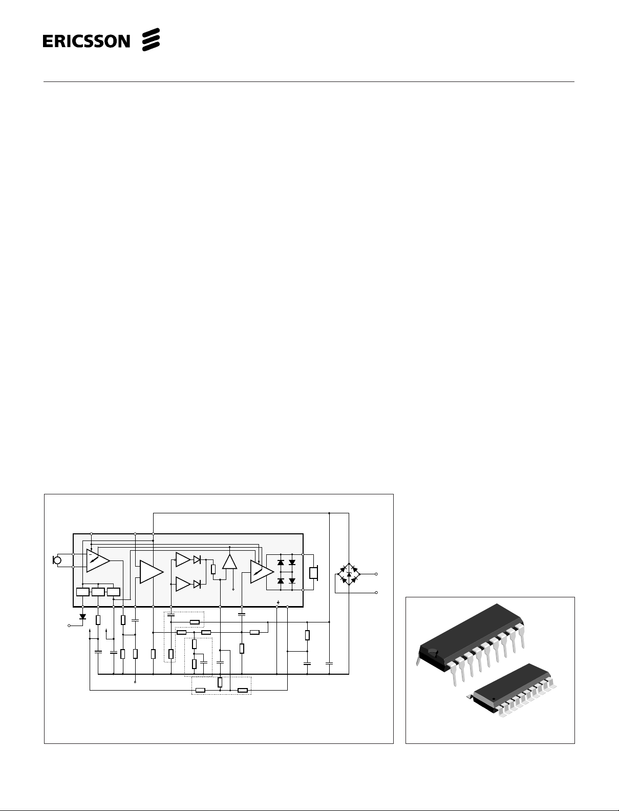
A. Dynamic limiter
B. Sidetone network
C. Gain regulation with line length
Figure 1. Functional diagram.
C.
(-Line)
PBL3852
18-pin plastic DIP 20-pin plastic SO
1
PBL 3852
Maximum Ratings
Parameter Symbol Min Max Unit
Line voltage, T
Line current, continuous DIP I
Line current, continuous SO package I
Operating temperature range T
Storage temperature range T
Input level (all inputs) 0+C V
R
feed
+
E= 48.5V
= 2 s V
p
MUTE
R = 0-4KΩ
L
0 ohm when artificial
line is used
5H+5H
= 400Ω+400Ω
C = 1µF when artificial line is used
470µF when no artificial line
+
C
V
600Ω
2
V
1
ARTIFICIAL
LINE
I
L
V
V
DC2
L
V
M
+ LINE
I
DC2
I
DC1
V
DC1
PBL 3852
with external
components
See fig. 4
MIC
REC
V
4
- LINE
L
L
L
Amb
Stg
Z
= 150Ω
Mic
V
3
Z
= 150Ω
Rec
022 V
0 130 mA
0 100 mA
-40 +75 °C
-55 +125 °C
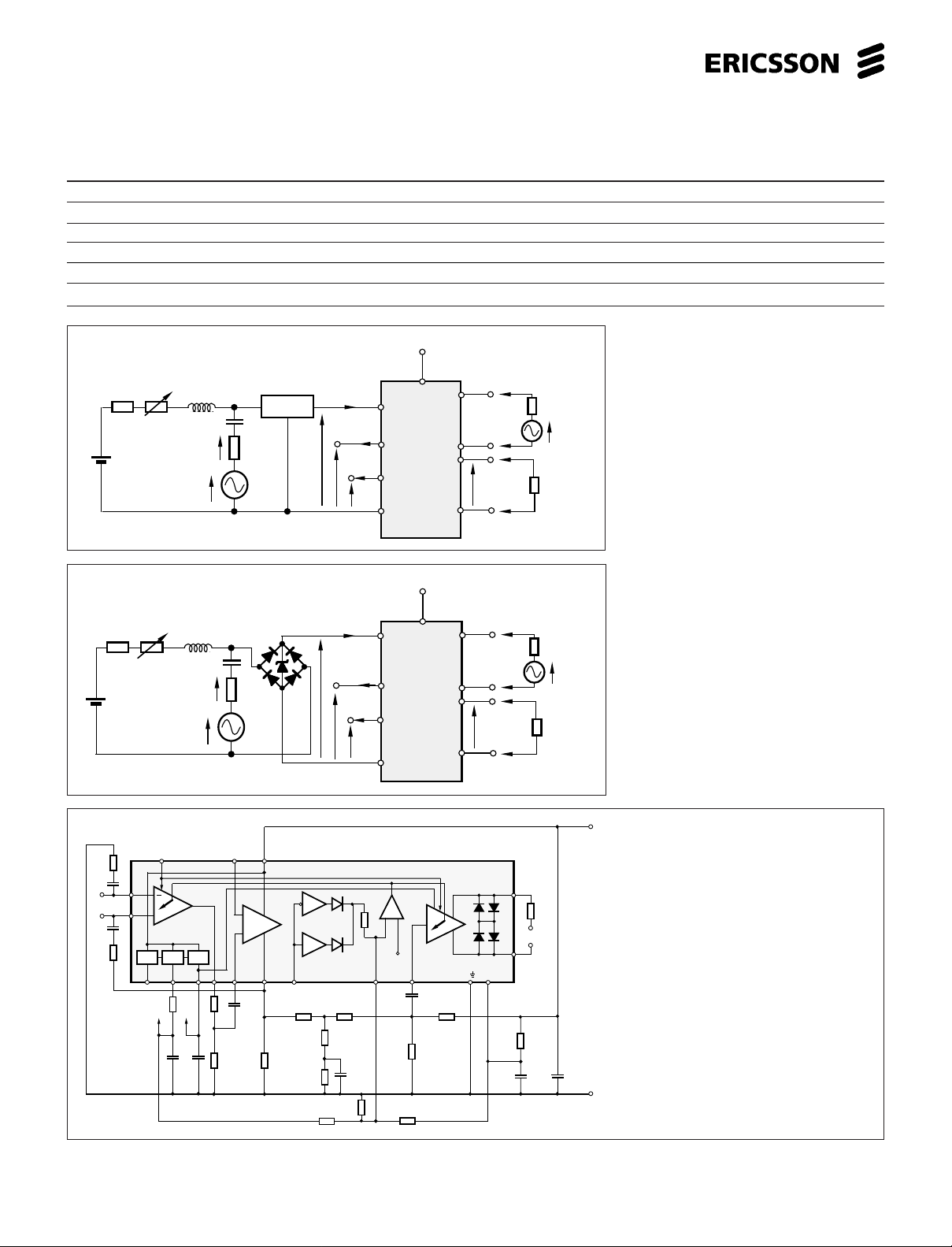
Figure 2. Test set up without rectifier
bridge.
MUTE
V
M
R
+
E = 48.5V
= 400Ω+400Ω
feed
R = 0-4KΩ
L
5H+5H
V
V
1
1µF
2
Uz= 15-16V
+
600Ω
I
L
+ LINE
PBL 3854
with external
components
See fig. 4
MIC
REC
V
4
V
L
I
DC2
V
DC2
I
DC1
V
DC1
Z
= 150Ω
Mic
V
3
Z
= 150Ω
Rec
- LINE
Figure 3. Test set up with rectifier bridge.
REC
+
R24
C10
(+Line)
(-Line)
R22
C12
MIC
C13
R23
Mute
6
13
+
12
DC
Ref.
supply
18 9 8
R3
DC1 DC2
+
C2
C3
supply
DC
R4
+
5
3
11
R5 R7
1
27
C4
PBL 3852
R9 R11
R12
R13
R14
R15
17
-
+
+
Ref.
15
10
C8
R18
R17
C6
R16
16
14
4 +
R19
+C
C9
Figure 4. Reference figure with line length regulation. (Application for dynamic microphone)
R1 = - C1 = R2 = - C2 = 47µF
R3 = 100Ω C3 = 47µF
R4 = 7.5k C4 = 68nF
R5 = 33k C5 = R6 = - C6 = 100nF
R7 = 75Ω C7 = R8 = - C8 = 47nF
R9 = 620Ω C9 = 47µF
R10 = - C10 = 15nF
R11 = 6.2k C11 = R12 = 130Ω C12 = 0.15µF
R13 = 2.4k C13 = 0.15µF
R14 = 27k
R15 = 18k
R16 = 120k
R17 = 18k
R18 = 62k
R19 = 910Ω
R20 = R21 = R22 = 10k
R23 = 10k
R24 = 150Ω
2

Electrical Characteristics
At T
= + 25° C. No cable and no line rectifier unless otherwise specified.
Amb
PBL 3852
Parameter fig. Conditions Min Typ Max Unit
Line voltage, V
note 1 2 IL = 15 mA 3.3 3.7 4.1 V
L
Transmitting gain, note 1 20 •
Transmitting range of 2 1 kHz, R
regulation
note 1
Ref.
2I
2R
2R
2R
= 100 mA 11 13 15 V
L
10
log (V2 / V3); 1 kHz
= 0 414345dB
L
= 400Ω 43.5 45.5 47.5 dB
L
= 900Ω - 2200Ω 46 48 50 dB
L
= 0 to 900 ohm 3 5 7 dB
L
Transmitting frequency 2 200 Hz to 3.4 kHz relative to 1 kHz -1 1 dB
response
Receiving gain, note 1 20 •
2R
2R
2R
Receiving range of regulation 2 1 kHz, R
10
log (V4 / V1); 1 kHz
= 0Ω -13 -11 -9 dB
L
= 400Ω -10.5 -8.5 -6.5 dB
L
= 900Ω - 2200Ω -8 -6 -4 dB
L
= 0 to 900Ω 357dB
L
Receiving frequency response 2 200 Hz to 3.4 kHz relative to 1kHz -1 1 dB
Microphone input impedance 2 1 kHz, 1.7 kΩ
pin 12 (14),13 (15)
Transmitter input impedance 2 1 kHz 17 kΩ
pin 3
Transmitter dynamic output 2 200 Hz - 3.4 kHz 1.5 V
≤ 2% distortion, IL = 20 - 100 mA
Transmitter max. output 2 200 Hz - 3.4 kHz 3 V
IL = 0 - 100 mA, V3 = 0 - 1 V
Receiver output impedance 2 1 kHz, R
= 0Ω, note 4 32(+150) Ω
L
Receiver dynamic output 2 200 Hz - 3.4 kHz 0.5 V
≤ 2% distortion, IL = 20 - 100 mA
Receiver max. output 3 Measured with line rectifier 0.9 V
200 Hz - 3.4 kHz, IL = 0 - 100 mA
V
= 0 - 50 V
Transmitter output noise 2 Psoph-weighting, Rel 1 V
Receiver output noise 2 A-weighting, Rel 1V
1
rms
, RL = 0 -75 dB
rms
, with cable -80 dB
0 - 5 km, ø = 0.5 mm note 3
0 - 3 km, ø = 0.4 mm
Mute input current 2 20 µA
DC1-supply voltage 2 I
DC2-supply voltaget (clamp) 2 I
= (20 - 100) mA note 2 1.75 2.0 2.25 V
L
I
= 1 mA
DC1
= 20-100 mA see text, I
L
= 1.9 mA note 2 3.4 3.7 4.0 V
DC2
at zero signal in the receiver amplifier
p
p
p
p
Psoph
A
Notes
1. Adjustable to both higher and lower values with external components.
2. Lowest line current dependent of the set DC-characteristic. See page 14, fig 8.
3. Psofometric weighting will give (6-7) dB lower value. (-dB)
4. 150 ohm resistor in test set up.
3
PBL 3852
Pin Description
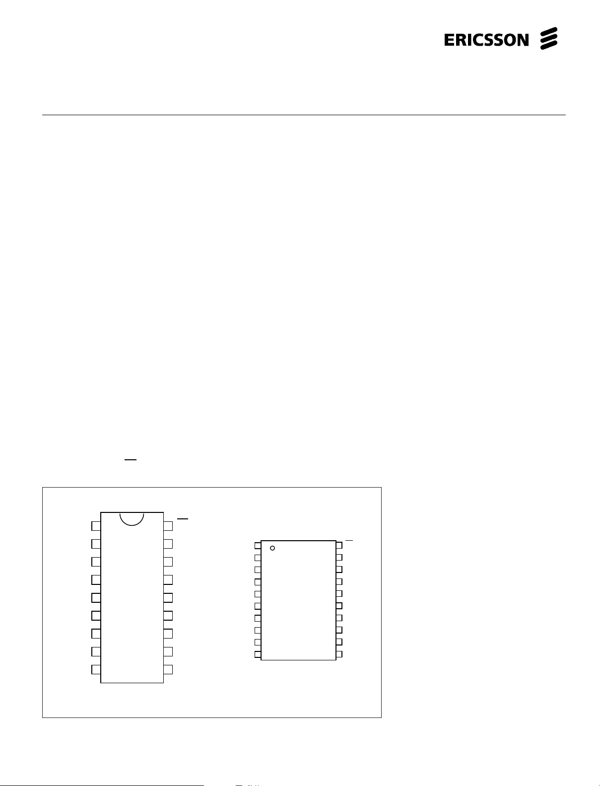
DIP SO Symbol Description
1 1 +L Positive line terminal
2 2 TO Slope setting for DC characteristic and sidetone balancing signal output
3 3 TI Transmitter amplifier input
4 4 +C Internal power supply
5 5 DCC Line voltage DC level adjustment input
6 6 MUTE Transmitter and receiver amplifier mute input
7 7 RCT Dynamic limiter ”soft clipping” input
8 8 DC2 DC supply 2 output, typically 3.7 V
9 9 DC1 DC supply 1 output, typically 2.1 V
10 NC Not connected
11 NC Not connected
10 12 GR The output of the rectifier to the dynamic limiter and gain regulation input
11 13 MO Microphone amplifier output
12 14 MI1 Microphone amplifier non-inverting input
13 15 MI2 Microphone amplifier inverting input
14 16 -L Negative line terminal
15 17 RI Receiver amplifier input
16 18 RO1 Receiver amplifier inverting output
17 19 RO2 Receiver amplifier non-inverting output
18 20 PD Power down input
+L
1
TO
2
TI
3
+C
4
DCC
5
6
Mute
7
RCT
8
DC2
DC1 GR
9 10
18
17
16
15
14
13
12
11
PD
RO2
RO1
RI
-L
MI 2
MI 1
MO
TO
+C
DCC
Mute
RCT
DC2
DC1
+L
NC
1
2
3
TI
4
5
6
7
8
9
10
20
PD
19
RO2
18
RO1
17
RI
16
-L
15
MI 2
14
MI 1
13
MO
12
GR
11
NC
DIP SO
Figure 5. Pin configuration.
4
Functional Description
Design procedure
1. Set the circuit impedance to the line,
either 600Ω or complex. (R19 and C9).
C9 should be big enough to give low
impedance compared with R19 in the
telephone speech frequency band.
Too large C9 will make the start-up
slow.
2. Set the DC-characteristic that is
required in the PTT specification or in
case of a system telephone in the PBX
specification (R7). There are also
internal circuit dependent requirements
like supply voltages etc.
3. Set the attac point where the line length
regulation is supposed to cut in
(R14,R15 and R16). Note that in some
countries the line length regulation is
not allowed. In most cases the
end result is better and more readily
achieved by using the line length
regulation (line loss compensation)
than without.
4. Set the transmitter gain, regulation and
frequency response. See text for the
dynamic limiting feature.
5. Set the receiver gain and frequency
response. See text how to limit the
max. swing to the earphone.
6. Adjust the side tone balancing network.
7. Set the RFI suppression components
in case necessary. In two piece
telephones the often ”helically” wound
cord acts as an aerial where especially
the microphone input with its high gain
and input impedance is the more
sensitive.
+Line
1
2
R7
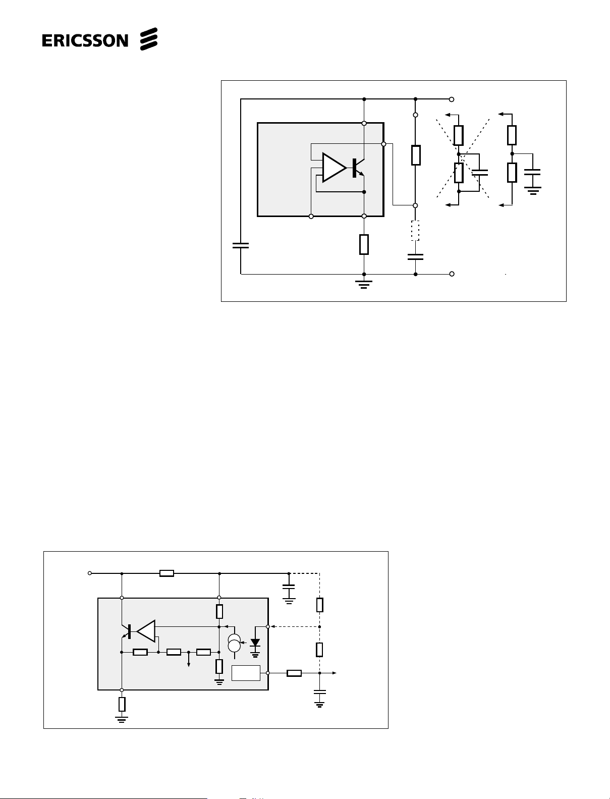
Figure 7. System of DC-Characteristic.
R19
PBL 3852
+
-
Ref=1.16V
PBL 3852
1
4
3
C10
2
R7
Figure 6. AC-impedance.
Impedance to the line
The AC- impedance to the line is set by
C10, R19 and C9. Fig. 6. The circuits
relatively high (≈ 20k with R7 = 75Ω)
parallel impedance will influence it to
some extent. At low frequencies the
influence of the C9 can not be neglected.
Series resistance of the C9 that is
dependent on temperature and quality will
cause that some of the line signal will
enter pin 4 and generate a closed loop in
the transmitter amplifier that will create an
active impedance thus lowering the
impedance to the line. The impedance at
high frequencies is set by C10 that also
acts as a RFI suppressor.
In many specifications the impedance
towards the line is specified as a complex
network. See fig. 6. In case a) the error
+
C9
4
- I pin5
DCsupply
5
I pin5
9
R3
+
R20
R21
DC1
C2
PBL 3852
+Line
a) b) c)
R19
Rs
≈1Ω
+
signal entering pin 4 is set by the ratio
≈Rs/R19 (909Ω), where in case b) the
ratio at high frequency will be Rs/220Ω
because the 820Ω resistor is bypassed by
a capacitor. To help up this situation the
complex network capacitor is connected
directly to ground, case c) making the
ratio Rs/220Ω+820Ω and thus lessening
the error signal. Conclusion: Use case c)
when complex impedance is specified.
DC - characteristic
The DC - characteristic that a telephone
set has to fulfill is mainly given by the
network administrator.Following parameters are useful to know when the DC
behaviour of the telephone is to be set:
• The voltage of the feeding system
• The line feeding resistance 2 x.... ohms
• The maximum current from the line at
zero line length
• The min. current at which the telephone
has to work (basic function)
• The lowest and highest voltage
permissible across the telephone set.
• The highest voltage that the telephone
may have at different line currents is
normally set by the network owners
specification. The lowest voltage for the
telephone is normally set by the
different voltages that are needed for
the different parts of the telephone. For
ex. for transmitter output amplifier,
receiver output amplifier, dialler,
speech switching and loudspeaker
amplifier in a handsfree telephone etc.
Example:
The complex network
220Ω + 820Ω//115nF
C9
-Line
5
PBL 3852
V
16
14
12
10
8
6
4
2
20 40 60 80 100 120
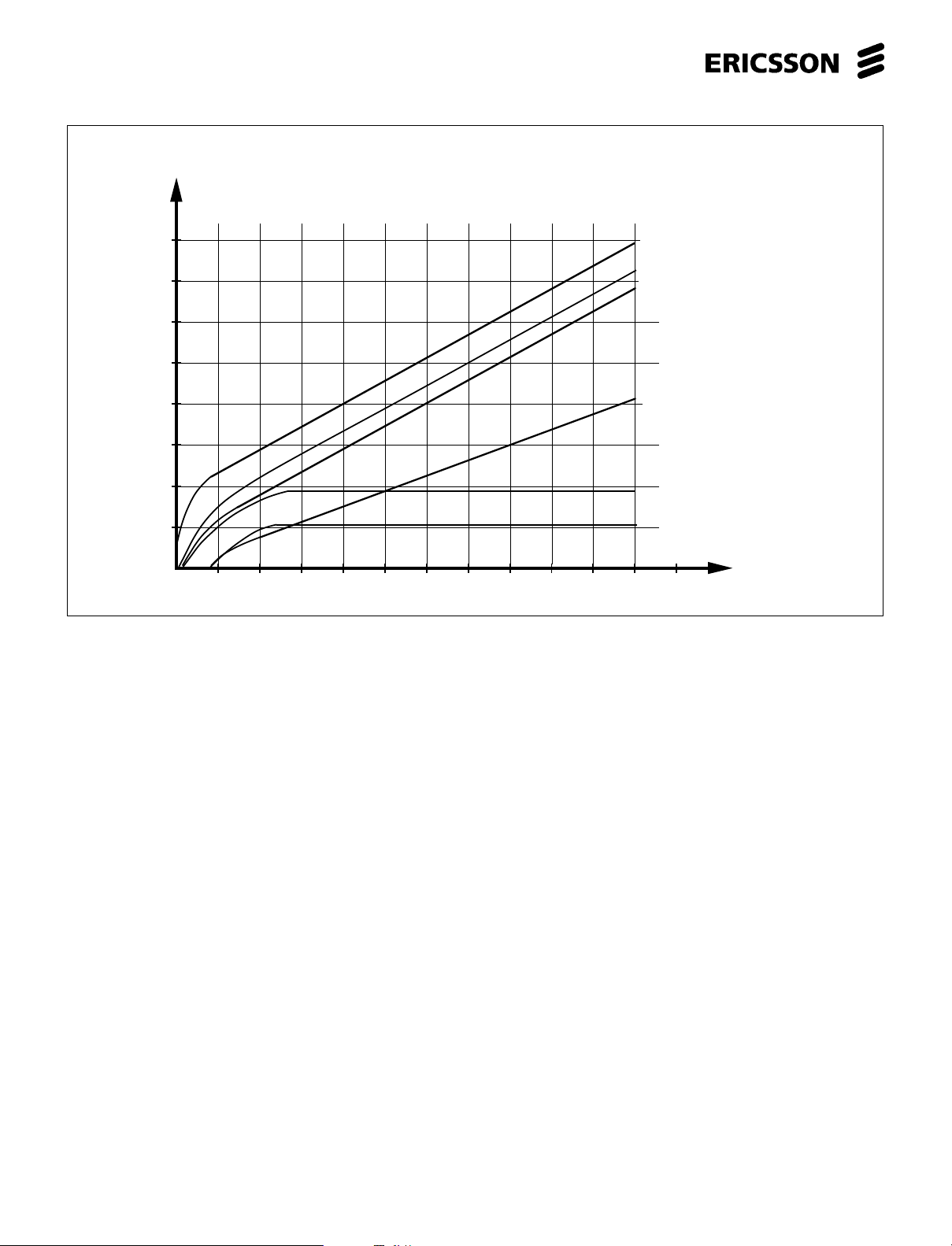
Figure 8. DC-Characteristics. (R7 = 75 Ω)
V
circ
. =
I
PIN
4
⋅
R
19
+k1⋅
Vref+R
a
=
I
pin
5
⋅5.5⋅10
3
if function DC−control at pin5is used
()
7
⋅
V telephone line
V line
V pin 4
V pin 2
V pin 8
V pin 9
I
L
mA
I
line
+
k
2
⋅
V
pin
2
+
a
k
1
⋅
V
ref
= 1.1
V
k
2
⋅
V
pin
2
= 0.5⋅
I
PIN
4 ≈
1
mA
The R7 will set the slope of the DC-char.
and the rest of the level is set by some
constants in the circuits as shown in the
equation. The slope of the DC-char. will
also influence the line length regulation
(when used) and thus the gain of both
transmitter and receiver. R7 acts also as
current protection for the circuit, must be
considered when low values are to be
used. The level of DC-characteristic can
be adjusted up at input pin 5 (some
100mV´s). The R21 adjusts a fix amount
where R20 couples the adjusted value to
line current. See fig. 32.
Microphone amplifier
The microphone amplifier in the PBL
3852 is divided into two stages. The first
stage is a true differential amplifier
providing high CMRR (-55 to -65 dB
R
7
⋅
I
line
typical) with voltage gain of 19 dB. This
stage is followed by a gain regulated
amplifier with a regulation range from 6.5
dB to 14.5 dB, see fig. 15. The input of
the microphone amplifier can be used for
electret, magnetic or dynamic transducers
see fig. 9. The PBL 3852 has basically a
higher gain regulation range (8 dB) than
the more or less standard 6 dB´s for gain
regulation with line length, this in order to
be able to be used in applications where
”softclipping” is required. In case lower
regulation range is necessary, it is
possible with some additional
components.
See reference figs. 4, 10c, 10f, 32 and
33. For an electret microphone the
circuitry will be simple, see fig. 10f. A
resistor is added from the microphone
amplifier output, pin 11, to the positive
termination of the microphone and further
via a capacitor to the - input at pin 13.
The DC supply resistors for the
microphone should be round 200Ω (in
order not to overdrive the microphone
amplifier) and the feedback resistor (17k)
is of that magnitude that it either
influences the CMRR balance at the
input or destroys the send mute by
bypassing signal round the microphone
amplifier in mute state. For a dynamic
microphone some more components are
necessary, see fig. 10c. In order not to
influence the send mute the feedback
signal is taken from transmitter output at
pin 2 and because this signal is in
opposite phase with the signal at pin 11,
it is taken to the other input at pin 12. Also
in order not to influence the DC-balance
of the microphone amplifier a capacitor
has to be included in the feedback path
and to maintain the CMRR of the
6
PBL 3852
microphone amplifier a similar RC
combination ought to be connected from
the other input, pin 13, to ground.
An electret microphone with a built in
FET amplifier is to be seen from outside
as a high impedance constant current
generator and is normally specified with a
load resistance of ≈ 2k. This is to be
considered as max. value and by using it
will render the max. gain from the microphone. This level of input signal that is
unnecessary high will result in clipping in
the microphone amplifier and in mute
condition permeate through the input to
Strong
cc gen.
11
DCload
ACload
the circuits reference and this way to all
functions, resulting among other things in
a bad mute. Hence it is better regarding
noise perfomance and mute to rather use
the gain of the microphone amplifier than
the gain of the microphone itself (in case
of electret) flat out. A more suitable level
of gain from the microphone is achieved
by using a load resistance of 200 - 470Ω.
Gain setting to the line is done at the
input of the transmitter.
It is possible to use the microphone
amplifier as a limiter ( added to the limiter
in the transmitter output stage ) of the
DC ( ref. ≈ 1.16V )
ref. minus a diode ≈ 0.5V
DC-load = R4+R5
DTMF
) //Z
AC-load = R4+R5// (R6+Z
Z
DTMF
= DTMF generator impedance
TI
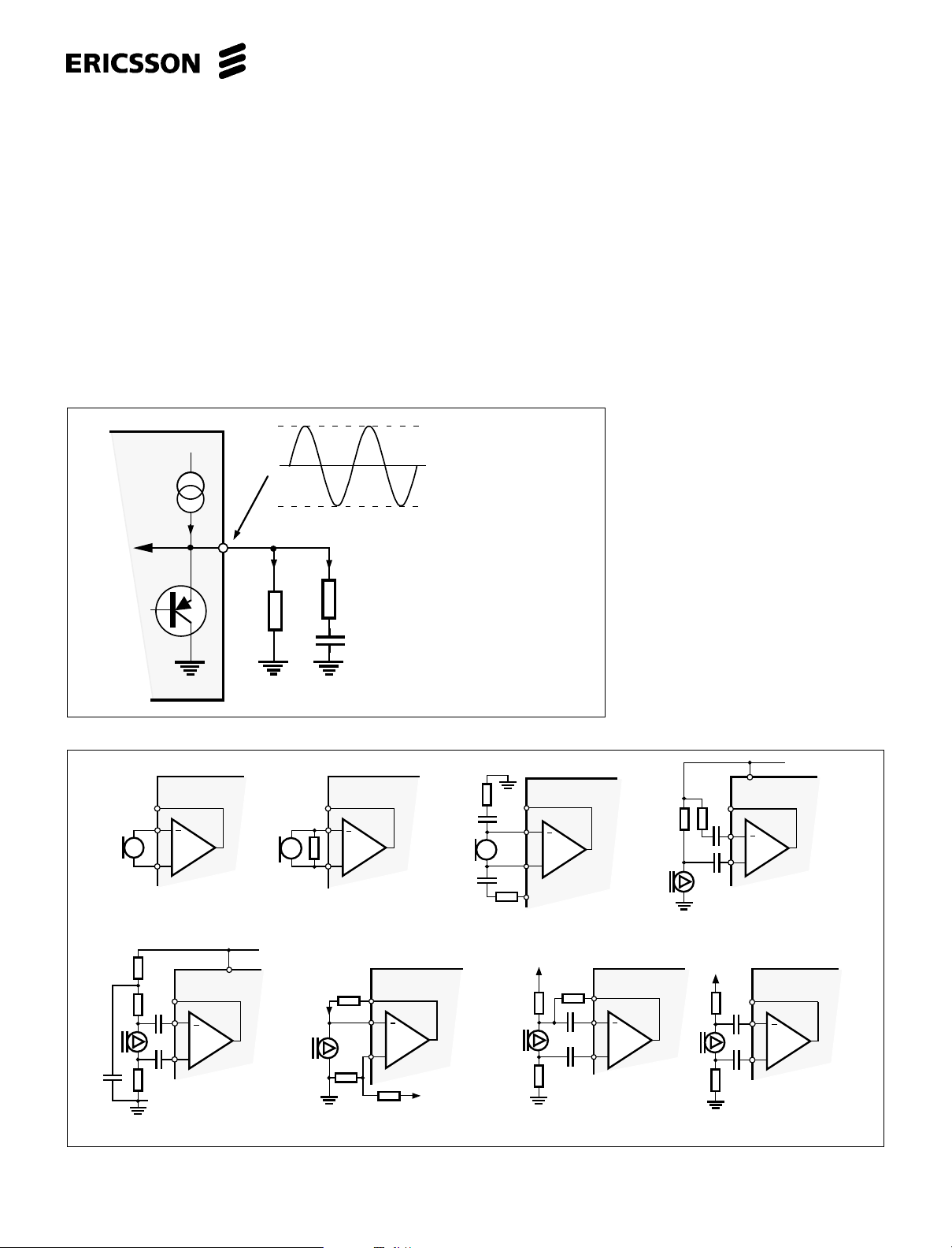
transmitted signal (See fig. 9). The
positive output swing is then limited by the
peak output current of the microphone
amplifier. The negative swing is limited by
the saturation voltage of the output
amplifier. The output of the amplifier is
DC-vice at internal reference level
(1.16V). The lowest negative level for the
signal is reference minus one diode and
sat. transistor drop (1.16-0.6-0.1 = 0.46V).
The correct clipping level is found by
determining the composite AC- and DCload that gives a maximum symmetrical
unclipped signal at the output. This signal
is then fed into the transmitter amplifier at
a level that renders a symmetrical signal
clipping on the line. (adjust with ratio R4,
R5) The total transmitter gain when an
electret microphone is used can then be
adjusted with the load resistor of the
electret microphones buffer amplifier.
Figure 9. Microphone amplifier output clipping.
(a)
R
C
+
PBL 3852
11
13
M
12
+
Dynamic
microphone
M
+
4
PBL 3852
(h)
11
13
12
Balanced electret microphone.
An additional RC filterlink is
recommended if pin 4 is used
as a supply.
(b)
11
13
12
+
Magnetic
microphone
(g)
Im
Rx
Mic. ampl. supplies the mic.
current Im, set by Rx and Ry.
Figure 10. Microphone solutions.
PBL 3852
M
11
13
12
PBL 3852
M
+
Unbalanced electret
microphone
Ry
DC1
(c)
PBL 3852
11
13
M
12
+
For dynamic mic.with
2
reduced gain
regulation
DC1
(f)
Balanced electret
microphone with reduced
gain regulation
PBL 3852
(d)
4
11
13
M
12
+
Unbalanced electret
mic. with balanced
signal, DC-supply from
pin 4.
DC1
PBL 3852
11
13
M
12
+
(e)
PBL 3852
11
13
M
12
+
Balanced electret
microphone
7
PBL 3852
(a),(c), (d)
(b),(e)
(f)
big C
A
small C
A
Transmitter amplifier
The transmitter amplifier in PBL 3852
consists of three stages. The first stage is
an amplitude limiter for the input signal at
TI, in order to prevent the transmitted
signal to exceed a certain set level and
cause distortion. The second stage
amplifies further the signal from the first
and adds it to a DC level from an internal
DC-regulation loop in order to give the
required DC characteristic to the
telephone set. The output for this stage is
TO. The third stage is a current generator
that presents a high impedance towards
the line and has its gain from TO to +L.
The gain of this amplifier is ZL/R7 where
ZL is the impedance across the telephone line. Hence, the absolute maxi-
11 3
R
A
(a)
C
A
11
(b)
R
A
C
mum signal amplitude that can be
transmitted to the line undistorted is
dependent of R7.(amplitude limiting) The
figure 20 shows the range for the
amplitude limiter dependent of the
operating point on the DC characteristic.
The transmitter gain and frequency
response are set by the RC-network
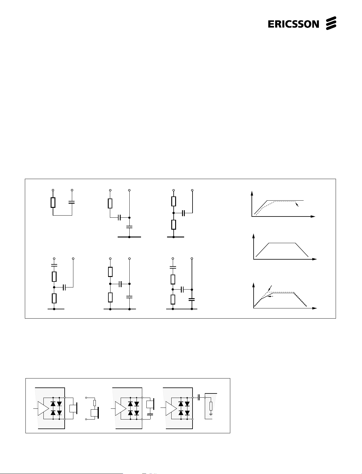
between the pins MO and TI (See fig. 11).
The capacitor for cutting the high
frequency end is best to be placed directly
at the microphone where it will also act as
a RFI suppressor. The input signal source
impedance to the transmitter amplifier
input TI should be reasonably low in order
to keep the gain spread down, saying that
R4//R5//R6 (see fig. 32) must be at least a
factor of 5 lower than the ZTin. Observe
that the capacitor C9 should have a
3
A
11
3
(c)
R
A
C
A
reasonably good temperature behaviour
in order to keep the impedance rather
constant. The V+C´s influence on the
transmitter DC-characteristic is shown in
the fig. 8 therefore the transmitter gain
would change if the transmitted signal
gives reason to an ac-voltage leak signal
across C9, this being a feedback point. If
the transmitter has an unacceptable low
sving to the line at low line currents
<≈10mA the first should be to examine if
the circuits DC- characteristic can be
adjusted upwards and first secondly make
use of the linear PD.
no attn.
11
(d)
C
C
R
A
C
A
R
B
attn.without dc.
C
no attn.
3
11
B
3
(e)
R
A
C
A
R
C
B
B
attenuation
R
B
attenuation
11
(f)
C
C
R
A
C
A
R
C
B
B
attn.without dc.
3
Figure 11. Different possible types of networks between microphone amplifier and transmitter.
Receiver amplifier
The receiver amplifier consists of three
stages, the first stage being an input
buffer that renders the input a high
impedance. The second stage is a gain
(a)
+
17
-
Rx
+
16
(b)
≈150Ω
150Ω
regulated differential amplifier and the
third stage a balanced power amplifier.
The power amplifier has a differential
output that does not need a series
capacitor with the load. The receiver
(c)
17
-
+
Rx
+
16
(d)
17
-
+
+
Rx
+
16
Z
amplifier uses at max. swing (4-6) mA
peak. This current is drawn from DC2
that can supply 2 mA continuous
current, the C3 helping to supply the
peaks, this applies for speech signals
only. Continuous sinusoidal signals at
this level will load the DC2 down. If a
distortion appears in the earphone
amplifier output at high signal levels,
high line currents, low ohmic earphone
load or at low frequencies, the most
probable fault is that the filtering
capacitor of the earphone amplifier
supply C3 is too small. At low line
Figure 12. Receiver arrangements.
8
currents (normal case, IL < 10 mA)
 Loading...