

Maintenance Manual
LBI-38735B
M-RK
UHF
PERSONAL TWO-WAY FM
RADIO COMBINATION
ericssonz
TABLE OF CONTENTS
Service Assemblies...................................................................LBI-3 8746
Service Section............. ... .........................................................LBI-3 8740
Disassembly and Assem bly.............. ........ ........ ........... ........ .....LBI-38741

LBI-38735
NOTICE!
This manual cove rs Eri c sson and Gene ra l Elect ric pro duc ts m an ufa ctured and sold by Eri csson In c.
NOTICE
Repairs to this equipment should be made only by an authorized service technician or facility designated by the supplier. Any
repairs, altera tions or substi tut io n of rec om m e nde d pa rts m ad e by the user to this eq uipment not approved by the ma nufa c tu re r
could voi d the user’s authority to opera te the equipment in add it ion to the ma nufacture r’ s w ar ra nty.
NOTICE
The software contained in this device is copyrighted by Eri csson Inc. Unpublished rights ar e reserv ed under the copyr ight
laws of the United States.
This manual is published by Ericsson Inc., without any warranty. Improvements and changes to this manual necessitated by
typographical errors, inaccuracies of current information, or improvements to programs and/or equipment, may be made by
Ericsson Inc., at any time and without notic e. Such cha nge s will be inco rpor ta ted int o new ed it ion s of this manual . No part of
this manual may be reproduced or transmitted in any form or by any means, electronic or mechanical, including photocopying
and recording, for any purpose, without the express written permission of Ericsson Inc.
Copyright © May 1993, Ericsson GE Mobile Communications Inc.
2

LBI-38735
TABLE OF CONTENTS
Page
SPECIFICATIONS . . . . . . . . . . . . . . . . . . . . . . . . . . . . . . . . . . . . . . . . . . . . . . . . . . 4, 5
DESCRIPTION . . . . . . . . . . . . . . . . . . . . . . . . . . . . . . . . . . . . . . . . . . . . . . . . . . . . 6
RADIO ASSEMBLY . . . . . . . . . . . . . . . . . . . . . . . . . . . . . . . . . . . . . . . . . . . . . . . . . 7
TRANSMIT CIRCUIT . . . . . . . . . . . . . . . . . . . . . . . . . . . . . . . . . . . . . . . . . . . . . 7
RECEIVE CIRC UIT . . . . . . . . . . . . . . . . . . . . . . . . . . . . . . . . . . . . . . . . . . . . . . 8
FREQUENCY SYNTHESIZER . . . . . . . . . . . . . . . . . . . . . . . . . . . . . . . . . . . . . . . . 8
LOGIC CIRCUIT . . . . . . . . . . . . . . . . . . . . . . . . . . . . . . . . . . . . . . . . . . . . . . . . 8
SYSTEM ANALYSIS . . . . . . . . . . . . . . . . . . . . . . . . . . . . . . . . . . . . . . . . . . . . . . . . . 8
RADIO BOARD ASSEMBLY. . . . . . . . . . . . . . . . . . . . . . . . . . . . . . . . . . . . . . . . . . 8
Transmit Circuits . . . . . . . . . . . . . . . . . . . . . . . . . . . . . . . . . . . . . . . . . . . . 8
Power Amp li fier Module (U7) . . . . . . . . . . . . . . . . . . . . . . . . . . . . . . . . . . 8
LPF/DC/T/R SW Module (U8) . . . . . . . . . . . . . . . . . . . . . . . . . . . . . . . . . . 9
Receive Circuit . . . . . . . . . . . . . . . . . . . . . . . . . . . . . . . . . . . . . . . . . . . . . 9
RF Amplifie r/Mixer . . . . . . . . . . . . . . . . . . . . . . . . . . . . . . . . . . . . . . . . 9
First IF Amplifier . . . . . . . . . . . . . . . . . . . . . . . . . . . . . . . . . . . . . . . . . 9
Second IF Amplifier/Discriminator (U11) Non-switchable . . . . . . . . . . . . . . . . . . . 9
Second IF Amplifier/Discri m ina t or (U11) Switchable . . . . . . . . . . . . . . . . . . . . . . 9
Synthesiz e r Circuit . . . . . . . . . . . . . . . . . . . . . . . . . . . . . . . . . . . . . . . . . . . 9
Phase-Lock -Loop Module (U2) . . . . . . . . . . . . . . . . . . . . . . . . . . . . . . . . . . 9
Voltage-Contro ll ed Oscillator (U5) . . . . . . . . . . . . . . . . . . . . . . . . . . . . . . . . 10
VCTCXO Reference Oscillator (Z1) . . . . . . . . . . . . . . . . . . . . . . . . . . . . . . . 10
LOGIC CIRCUIT . . . . . . . . . . . . . . . . . . . . . . . . . . . . . . . . . . . . . . . . . . . . . . . . 10
Control Board Assembly. . . . . . . . . . . . . . . . . . . . . . . . . . . . . . . . . . . . . . . . 10
Microcomputer . . . . . . . . . . . . . . . . . . . . . . . . . . . . . . . . . . . . . . . . . . 10
2
Flash E
RAM (U5) . . . . . . . . . . . . . . . . . . . . . . . . . . . . . . . . . . . . . . . . . . . . . 11
E
Digital Signal Processor (DSP)(U3) . . . . . . . . . . . . . . . . . . . . . . . . . . . . . . . 11
Voltage Regulator (U9, U10) . . . . . . . . . . . . . . . . . . . . . . . . . . . . . . . . . . . 11
Audio Am pl ifi er (U11) . . . . . . . . . . . . . . . . . . . . . . . . . . . . . . . . . . . . . . 11
Audio Signal Processor (ASP)(U7) . . . . . . . . . . . . . . . . . . . . . . . . . . . . . . . . 11
LED Flex Asse mb ly (M-RK I) . . . . . . . . . . . . . . . . . . . . . . . . . . . . . . . . . . . . 17
LCD/KB Flex Assembly (M-RK I I & Scan) . . . . . . . . . . . . . . . . . . . . . . . . . . . . . 17
Keypad (M-RK I I & Scan) . . . . . . . . . . . . . . . . . . . . . . . . . . . . . . . . . . . . . . 17
UDC . . . . . . . . . . . . . . . . . . . . . . . . . . . . . . . . . . . . . . . . . . . . . . . . . . 17
PROM (U4) . . . . . . . . . . . . . . . . . . . . . . . . . . . . . . . . . . . . . . . 11
2
PROM (U6) . . . . . . . . . . . . . . . . . . . . . . . . . . . . . . . . . . . . . . . . . . 11
MAINTENANCE . . . . . . . . . . . . . . . . . . . . . . . . . . . . . . . . . . . . . . . . . . . . . . . . . . . 18
INITIAL ADJUSTME NT . . . . . . . . . . . . . . . . . . . . . . . . . . . . . . . . . . . . . . . . . . . . 18
Transmit Circuit Alignment . . . . . . . . . . . . . . . . . . . . . . . . . . . . . . . . . . . . . . 18
Receive Circuit . . . . . . . . . . . . . . . . . . . . . . . . . . . . . . . . . . . . . . . . . . . . . 18
Synthesiz e r Circuit . . . . . . . . . . . . . . . . . . . . . . . . . . . . . . . . . . . . . . . . . . . 18
3

LBI-38735
PREVENTIVE MAINTENANCE . . . . . . . . . . . . . . . . . . . . . . . . . . . . . . . . . . . . . . . 18
DISASSEMBLY . . . . . . . . . . . . . . . . . . . . . . . . . . . . . . . . . . . . . . . . . . . . . . . . . 18
REPLACEMENT . . . . . . . . . . . . . . . . . . . . . . . . . . . . . . . . . . . . . . . . . . . . . . . . 18
TROUBLESHOOTI NG PR OCEDURE . . . . . . . . . . . . . . . . . . . . . . . . . . . . . . . . . . . . 19
WEATHERPROOF INTEGRIT Y . . . . . . . . . . . . . . . . . . . . . . . . . . . . . . . . . . . . . . . 19
DIAGRAMS
Figure 1 - M-RK I Cont rols and Acc essories . . . . . . . . . . . . . . . . . . . . . . . . . . . . . . . . . . 7
Figure 2 - M-RK II & Scan Controls and Accessories . . . . . . . . . . . . . . . . . . . . . . . . . . . . . 7
Figure 3 - Radio Bloc k Diagram VHF/UHF (No n-switchable) . . . . . . . . . . . . . . . . . . . . . . . . 12
Figure 4 - Radio Block Diagram VHF/UHF (Swi tc ha bl e ) . . . . . . . . . . . . . . . . . . . . . . . . . . . 12
Figure 5 - M-RK I (Conv/EDACS) Lo gic Block Diagram . . . . . . . . . . . . . . . . . . . . . . . . . . . 13
Figure 6 - M-RK I (AEGIS) Logic Bloc k Diagram . . . . . . . . . . . . . . . . . . . . . . . . . . . . . . . 13
Figure 7 - M-RK II & Scan (Conv/ EDACS) Logic Block Diagram . . . . . . . . . . . . . . . . . . . . . . 14
Figure 8 - M-RK II & Sca n (AEGIS) Logic Block Diagram . . . . . . . . . . . . . . . . . . . . . . . . . . 14
Figure 9 - Power Amplifier (PA) UHF . . . . . . . . . . . . . . . . . . . . . . . . . . . . . . . . . . . . . 15
Figure 10 - LPF/ DC/ T/R SW Modu le (U8) VHF/UHF . . . . . . . . . . . . . . . . . . . . . . . . . . . . 15
Figure 11 - RF Amplifier/Mixer . . . . . . . . . . . . . . . . . . . . . . . . . . . . . . . . . . . . . . . . . 15
Figure 12 - First IF Amplifie r . . . . . . . . . . . . . . . . . . . . . . . . . . . . . . . . . . . . . . . . . . 15
Figure 13 - Second IF Am plifier/Discriminat or (Non-switchable) . . . . . . . . . . . . . . . . . . . . . . . 16
Figure 14 - Second IF Amplifier/Discri minator (Swit ch able) . . . . . . . . . . . . . . . . . . . . . . . . . 16
Figure 15 - Synthesizer . . . . . . . . . . . . . . . . . . . . . . . . . . . . . . . . . . . . . . . . . . . . . 17
TABLE OF CONTENTS (CONT.)
Antenna . . . . . . . . . . . . . . . . . . . . . . . . . . . . . . . . . . . . . . . . . . . . . . . . 18
Mechanica l Inspection . . . . . . . . . . . . . . . . . . . . . . . . . . . . . . . . . . . . . . . . . 18
Alignment . . . . . . . . . . . . . . . . . . . . . . . . . . . . . . . . . . . . . . . . . . . . . . . 18
Frequency Check . . . . . . . . . . . . . . . . . . . . . . . . . . . . . . . . . . . . . . . . . . . 18
SYSTEM FCC DOC
Regulator y Num ber AXATR-202-A5(403 - 430 MHz) TR-202
Frequency Range 403 - 430 MHz
Frequenc y Stab il ity ±5 ppm
Dimensions (HxWxD) w/battery (Typical)
M-RK I (Medium Capacity Bat tery) 161.8 mm x 68 mm x 30 mm
(High Capacity Battery) 176.8 mm x 68 mm x 30 mm
(Extra High Capaci ty Ba t te ry) 194.3 mm x 68 mm x 30 mm
4
SPECIFICATIONS *
AXATR-202-A5 (440 - 470 MHz) TR-202
AXATR-202-A5 (470 - 500 MHz) TR-202
AXATR-202-A5 (378 - 403 MHz)
440 - 470 MHz
470 - 500 MHz
378 - 403 MHz
±2 ppm (switchable)

LBI-38735
M-RK II & Scan (Medium Capa ci ty Batte ry ) 161.8 mm x 68 mm x 40.6 mm
(High Capacity Battery) 176.8 mm x 68 mm x 40.6 mm
(Extra High Capacity Battery) 194.3 mm x 68 mm x 40.6 mm
Weight
M-RK I (Medium Capaci ty Batte ry) 15.2 ounces
(High Capacity Batte ry) 19.2 ounces
(Extra High Capac i ty Ba ttery) 21.2 ounces
M-RK II & Scan (Me dium Capacity Battery) 16.4 ounces
(High Capacity Bat te r y) 20.4 ounces
(Extra High Capacity Battery) 22.4 ounces
Operable Temperature Range -30° to +60° (-22° to + 1 4 0 ° F)
TRANSMIT
RF Power Output 0.5 to 5 watts
Spurious Emissions -75 dBc
Maxim um Deviation ±5 kHz
±2.5 kHz (switcha bl e, narr owba nd m ode )
FM Hum & Noise -45 dB non-swit c hable , switcha bl e (wideba nd mod e)
-39 dB switcha ble (na rr owba nd mode)
Audio Distort ion <3% (60% Modulation)
Frequenc y Stab il ity ±5 ppm (-30°C to +60°C )non -swit ch ab le
±2 ppm (-30°C to +60°C )swit ch ab le
RF Load Impeda nc e 50 ohms
Microphon e Sensit ivit y Less than 90 dB SPL (EIA 60% MDD)
Maximum At ta c k Time 25 millisec onds (PT T Pushed)
Audio Frequenc y Re spon se Wit hi n +1 and -3 dB of a 6 dB/octave pre -e mphasis from 300 Hz to
3000 Hz. Non-swit chab le , switc ha bl e (wide ba nd mode)
Wit hi n +1 and -3 dB of a 6 dB/oc ta ve pre -e m pha sis from 300 Hz to
2550 Hz. Switc habl e (narrowb an d mode ).
RECEI VE
Sensitivity (12 dB SINAD) -116 dBm
Spurious Response -72 dB (minimum)
Selectivity -75 dB (25 kHz)
-60 dB (12.5kHz ) switch ab le units onl y
Squelch Sensitivity 6 dB SINAD
Distortion (EIA 0.5 watt) 5%
Audio Freque nc y Respon se W it hi n +1 and -3 dB of a 6 dB/oc ta ve de-e mp ha sis from 300 Hz to
3000 Hz.
NOTE
Non-switchable UHF units are designed for 25 kHz channel spacing only. Switchable
units with the proper software and feature encryption can be used in 12.5 kHz channel
spa c ing system.
* These specifications are intended primarily for use by service personnel. Refer to the appropriate Spedivication Sheet for
comple t e sp e c ifi c at ions.
5

LBI-38735
DESCRIPTION
The M-RK Personal Radio is a high-quality, high-performance FM radio. The radio is synthesized and operates in
both trunked and conventional communication systems. The
trunked mode allows selection of either a communications
group or an individual radio within a system. Both the selected group and the individual radio are secured through
digital signaling.
In the conventional mode, the user selects a channel and
directly c o mmu nicate s o n t h at chan n el . A ch an nel is a t r an s mit/re c e ive ra dio freque nc y pa i r.
A group consists of several users with a common group
identification (ID). A radio may have several groups, but the
selected group determines who the unit can call at any specific time. In the trunked mode, a set of groups which communicate on a set of channels is called a system. In the
conventional mode, a system is a set of channels. A system
may consist of all trunking groups and channels, all conventional channels, or a mixture of both.
The M-RK Personal Radio is designed to operate in a
Digital Trunking System or as a conventional radio providing the following features.
In trunked mode:
• Programmable Multiple System Capability -- The
radio can operate on different trunked sites or on
different systems at the same site.
• Multiple Group Capability -- The radio can
communicate on several Groups within one trunked
system.
• Automatic Power Levels -- The desired power level on
each channel can be programmed into the radio
personality. Power level is automatically selected
dependent on the channel.
• Emergency feature -- An emergency group can be
programmed into the radio. This group is selected by
pressing the EMR button. This allows a user to
quickly reach this group and initiate the M-RK
emergency signalling .
• Simple Remote Control Capability -- A
speaker/microphone (which can also control PTT and
the volume level) can be connected through the UDC
(Universal De vi ce Connector).
• Surveillance Feature -- The display backlighting
(M-RK II & Scan) may be programmed on or off per
group. The side-tone beep, related to the operation of
the radio controls, is also capa ble of being disable d on
a group-by-group basis.
• Programmable through UDC -- The entire personality
of the radio is programmed through four connections
of the UDC.
• 3 LED (including 2 bi-color LEDs) Display (M-RK I)
-- These LEDs are used to exhibit the condition of the
radio. It shows Channel Guard on/off, transmit mode,
battery condition, scan mode, channel busy, and
digital/cle a r mo de condit io n, etc.
• 16 Character Dot Matrix Alphanumeric Crystal
Display (M-RK II & Scan) -- This display is used to
exhibit the condition of the radio. It shows channel
designation, Channel Guard or Digital Channel Guard
on/off, transmit mode, volume lev el , battery condition,
channel busy, and high/low power output, etc.
• Group Call -- The M-RK has the capability of
simulta ne ou sly c al ling a ll uni ts wit hin a group.
• Programmable Carrier Control Timer -- Personality
information includes an optional period of transmit
time from 15 to 120 seconds. After the timer expires,
the unit will automatically unkey and provide an alert
tone. This feature is re-initiated on every PTT and the
alert ton e is re moved upon rele a se of the PTT.
• Minimum Volume Level -- Personality information
includ es a minimum volum e level.
• Programmable Squelch -- The noise squelch opening
threshol d can be pro gra mme d fo r each c ha nne l.
• Receive Mode Lock Out -- In normal trunked
operation, the radio will not transmit while in the
rece ive mode.
6
In conven tional mode:
• 16/192-Channel Capability -- Channel designation
can be a mixture of numerics (0-192) and
alphanumerics displayed through the LCD. Channel
control can come from the channel rotary switch, the
emergency channel feature, or the front keypad.
• Programmable Multi-Tone Channel Guard (CTCSS)
Encode/Decode -- Channel Guard tone frequencies
within the range of 67 Hz to 210.7 Hz, including all of
the standard EIA frequencies, may be programmed.
Different encode/decode, encode only, and
with/without Channel Guard frequencies are also
program m ab le int o the ra di o.
• Programmable Multi-Code Digital Channel Guard
(CDCSS) Encode/Decode -- Similar capability as with
T one Channel Guard is provi de d.

• Programmable Talkaround Capability -- The ability to
switch the transmit frequency from a repeater
frequency to a direct communications frequency.
• Channel-Busy Lock Out -- Personality information
includes the capability to prevent the transmitter from
operating on a channel where carrier activity is
present. The channel busy indicator (BSY) is active
during this time.
Physically an M-RK radio consists of three main printed
wire board assembli es and a battery pack as follows:
a. A printed wire board specially shielded with zinc al-
loy on which the radio assembly (transmit/re-
ceive/syn thesiz e r) i s assembl ed .
b. A Control bo ar d co nta i ning the microp roc e ssor.
c. A LCD/KB flex wire board with display processor,
rotary switc h, AF volume with switch.
d. A battery pac k that fit s the M-RK mai n uni t.
e. Lightweight plastic front and back housing.
LBI-38735
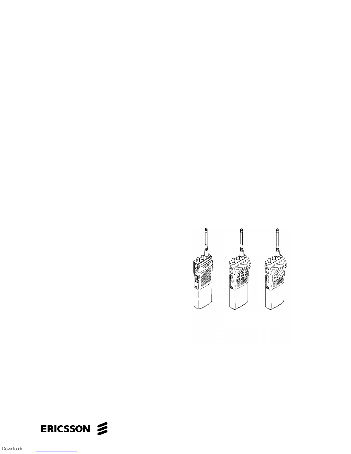
Figure 1 - M-RK I Control s and Accessories
Figure 2 - M-RK II & Scan Controls and Accessori es
RADIO ASSEMBLY
TRANSMIT CIRCUIT
The transmit circuit consists of four major circuits as fol-
lows:
a. Wide Band Amplifier -- Ampli fie s t he si gnal from the
frequency synthesizer.
b. Wide Band Power Amplifier -- Amplifies the output
signal of the amplifier to the desired output level for
transmi ssi on (a ga in of 38. 5 dB).
c. Wide Band Power Control Circuits -- Can reduce the
transmitter output level by 10 dB.
d. LPF, DC, Switch Hybrid Module -- Consists of LPF
and direct io na l coupl e r a nd T x/ Rx swit c h.
The transmitter completely covers the band within the
split. No adjustments are needed except for the RF power
control v oltage from the cont roller.
7

LBI-38735
RECEIVE CIRCUIT
The receiv er consists of th ree ma jor circ uit s as follows:
a. Front-End Circuit -- Consists of a one sta ge pre a mp li-
fier (with band-p ass fil te rs).
b. First Mixer and IF circuit -- A special double bal-
anced mixer is used to convert the incoming signal to
55.025 MHz first IF. This is put through a band-pass
filter (BPF) and an IF amplifi er to get the desi re d first
IF signal.
c. Second IF (455 kHz) -- Consists of one IC and three
BPF containing the second mixer, the second IF amplifier, and the FM detector. The second IF output
provides the Logic section with audio output.
FREQUENCY SYNTHESIZER
The frequency synthesizer is made up of three major
modules as foll ows:
a. VCO Module -- The UHF band frequency synthe-
sizer has one common VCO for both transmitting and
receiving. The transmitter is modulated at both the
VCO and the VCTCXO.
b. VCTCXO Module -- The VCTCXO is a voltage con-
trolled, temperature compensated crystal oscillator
providing 13.2 MHz (12.8 MHz for switchable models) as a reference frequency with modulation capability.
c. Phase-Lock Loop -- Consists of a frequency divider
and a low current drain CMOS IC for phase comparison.
Digital Signal Processor (DSP) -- Includes a modem,
address deco d er, and cloc k control circui t.
d. LED Flex Assembly (M-RK I) -- Includes LED dis-
play, rotary switch and AF volume with on/off
switch.
e. LCD/KB Flex Assembly. (M-RK II & Scan) -- In-
cludes LCD driver and processor for the display, rotary switch and AF vol um e wit h on /of f swit ch .
SYSTEM ANALYSIS
Refer to Figures 3 thru 8. The M-RK radio consists of
three major prin ted wir e boar ds as fol lows:
• Radio Board Assembly -- carries the tran smit, rec eive,
and freq uency synthesizer c ir cu it s.
• Control Board Assembly -- supports logic control
circuits.
• LED flex Assembly (M-RK I) -- ca rri es LEDs.
• LCD/KB flex Assembly (M-RK II & Scan) -- carries
LCD.
Interconnection of the control board with other boards
and control circuits is made with flexible circuit boards and
connectors.
Circuit illustrations shown are simplified representatives
of actual circuits. They are intended only to illustrate basic
circuit functi ons.
RADIO BOARD ASSEMBLY
Transmit Circuit s
LOGIC CIRCUIT
The logic circuit consists of a control board assembly
with an audio processor and a LED flex assembly (M-RK I),
LCD/KB flex assem bly (M-RK II & Scan) as follows:
a. Control Board Assembly -- Carries two microproces-
sors, RAM, Flash E
processor and I/O interconnections with the frequency synthesizer. This board commands all the
functions and operation of the M-RK radio.
b. Audio Signal Processor (ASP) -- Includes transmitter
and rec ei ve r a udi o ci rc uits.
c.
8
2
PROM, audio processor, digital
The M-RK transmit circuit, as shown in Figures 3 and 4,
consists of the following inte grated circ uit, modules.
• Power Amplifier (PA)
• LPF/DC/TR SW
Power Ampl ifier Module (U7)
Power Amplifier (PA) U7 is a four-stage, wideband amplifier module with an input and an output impedance of 50
ohms (Figure 9). The second stage of the PA module has the
dc power supplied by power set transistor Q203. The RF
power output from amplifier is connected to pin 1 of the PA
module where it is applied to the input of the RF power amplifier stages. The RF power amplifier stages amplify the input from the Tx-Amp module to a typical power output level

LBI-38735
of seven watts at pin 7. The output at pin 7 is connected
through the LPF/DC/SW module. A minimum power level o f
five watts is on the output of the LPF/ DC/SW module.
LPF/DC/T/R SW Modul e (U8 )
The output of the PA module is connected to
LPF/DC/SW. This network is a passive LC low-pass filter
with an insertion loss of less than 1.2 dB in the pass-band. It
also has a rejection greater than 50 dB in the stop band. The
output of this module is connected to the system antenna or
to the UDC connector.
Receive Circuit
The M-RK receive circuit, as shown in Figures 3 and 4,
consists of the following circuits:
• RF Amplifier/Mixe r
• First If Amplifier
• Second IF Am plifier/ Discrim inator
RF Ampl ifier/Mixer
The Rf Amplifier/Mixer circuit (Figure 11) contains two
third-order band-pass filters (FL301 and FL302), and RF
amplifier circuit (Q3O1) and a double-balanced diode mixer
circuit (Z2). RF from the antenna or UDC connector is coupled through LPF/DC/TR SW module to the input of the RF
amplifier circuit. The RF signal on the input of the RF amplifier is first coupled through band-pass filter FL301 to the
input of grounded emitter broad-band RF ampli fier transisto r
Q301. This amplifier provi des 1 3 d B o f p owe r g ai n to re duc e
thermal noise. The output of the RF amplifier is coupled
through band-pass filter FL3D2 to drive double balanced
mixer circuit Z2.
The RF signal from the RF amplifier and the injection
frequency from the synthesizer circuit, provide a 55.025
MHz IF on the output of the mixer. The double-balanced
Mixer has a typic al conversion loss of 7.5 dB betwee n the Rf
input and IF output. All inputs and the output of the RF Amplifier/Mixer have 50 ohms matching impedance. The +7
dBm injection frequency level, provided by the synthesizer
and amplifier circuit transistor Q103, is connected to the injection frequency input. The output of the Mixer circuit is
connecte d t o the inp ut of th e f irst IF Am pl if ie r.
First IF Am pli fier
The first IF amplifier contains a amplifier circuit and two
crystal filters of two poles, respectively (refer to Figure 12).
The first IF signal (55.025 MHz) connects to the input of
preamplifie r transistor Q302 through pre-cry stal filter FL303
with an impedance of approx im a te ly 3 Kohms. Pre-a m pl ifi e r
Q302 provides a 23 dB power gain. The output is connected
to the input of IF amplifier IC U11 through crystal filter
FL304.
Second IF Amplifi er/Disc rim inator (U11) Non-switchable
The Second IF Amplifier/Discriminator circuit (Figure
13) contains FM IF IC U11 and 455 kHz ceramic filters
FL305, FL306, FL307. The FM IF IC contains a local oscillator, mixer, IF amplifier, FM detector, and an audio amplifier. The 55.025 MHz IF output from the first IF amplifier is
connected to the input of second IF amplifier U11 pin 21
and converted to the second IF frequency (455 kHz). The
second IF output is connected to pin 7 input through the 45 5
kHz ceramic filter to the IF amplifier and FM detector circuits. The recovered audio from the FM IF IC is connected
to J1-3B.
Second IF Amplifi er/Disc rim inator (U11) Switchable
The Second IF Amplifier/Discriminator circuit (Figure
14) used in a switchable radio (25/12.5 kHz cha nne l spa c ing )
contains IC U11 and 455 kHz ceramic filters FL305, FL3 06,
FL307 and FL308 (used for 12.5 kHz channel spacing).
U11 contains a local oscillator, mixer, IF amplifier, FM detecto r an d an inverte r.
The 55.025 Mhz IF output from the first IF amplifier is
connected to the input of the second IF amplifier at U11-16.
There the mixer circuit converts the signal to the second IF
frequency (455 kHz). The second IF output at U11-3 is fed
through ceramic filters FL305 and FL306. Bi-lateral
switches U13 and U14 are controlled by the T/R switch and
25/12.5 kHz cont rols from the contr ol bo ar d.
When operation is selected for 25 kHz channel spacing,
the second IF frequency is passed by FL307 to U11-5 to the
IF amplifier and FM detector circuits. The recovered audio
is passed through bi-later al switch S12 to J1-3B.
When operation is selected for 12.5 kHz channel spacing,
the second IF frequency is passed by FL308 to U11-5 to the
IF amplifier and FM detector circuits. The recovered audio
is passed through bi-lateral switch S12 to U11-8. There the
audio passes through an inverter to the output of U11-7 and
then to J1-3B.
Synthesizer Circuit
The Synthesizer circuit (Figure 15) contains
Phase-Lock-Loop (PLL) module U2, VCTCXO Reference
Oscillator module Z1, TX/RX Voltage Controlled Oscillator
(VCO) module U5, and a Low-Pass-Filter (LPF) amplifier.
9

LBI-38735
The VCO used to generate the receive and transmit
frequencies is locked to a stable VCTCXO reference
oscillator through a PLL. This feed-back loop divides the
VCO frequency down to a signal in the range of 3.5 MHz.
This signal is divided with a programmable divider to 6.25
kHz, and generates a VCO control signal by comparing the
6.25 kHz feedback with a 6.25 kHz signal derived by
dividing a 13.2 MHz (12.8 MHz for switchable models)
VCTCXO by 2112 (2048 for switchable models). As the
least-significant bit i n the program m in g i s c ha nge d, the V C O
is forced to change by 6.25 kHz.
Transmi t audio fed into the synthesize r will be halv ed by
U4-2 in switchable radio units set for 12.5 kHz channel
spacing. This will limit voice deviation to a peak 2.25 kHz
and also halv e CG/DCG e nc ode de viat ion al so.
The synthesizer circuitry is contained on two modules,
the VCO module U5 and the VCTCXO reference oscillator
module Z1.
Phase-Lock-Lo op Mo dule (U2)
The PLL module U2 contains a reference frequency, divider, phase detector, and a program mable divider. The phase
detector dc voltage output signal is filtered with a passive
low-pass filter followed by a 6.25 kHz filter to reduce the
level of reference modulation on the VCO. This dc output
represents the error between the VCO frequency (phase) and
the reference (VCTCXO) and is applied to the VCO on frequency. A lock-detect output is developed from pin 9 of U2.
The output is "AND"ed with the TX-PTT output from the
microcompute r to prevent transmission before the VCO is o n
frequ ency.
Serial data from the microcomputer is shifted into the
PLL to set the division parameter which establishes the frequency. A clock signal is provided on another input and the
data is latched with the enable input.
VCTCXO Refer ence Oscillator (Z1)
The Z1 oscillator modul e is self contai ned, fully tem pera ture compensated and operates at a frequency of 13.2 MHz
(12.8 MHz for switchable models). The oscillator also has
modulation capability. Frequency is adjusted by a trimmer
while monitoring the transmit circuit output at the antenna
jack.
LOGIC CIRCUIT
The logic circuit consists of control circuits and audio
circuits (Figures 5 thru 8). Physically, this circuit consists of
two circuit board as follows:
• Control Bo ard Assem bly
• LED Flex Assembly (M-RK I)
• LCD/KB flex Assembly (M-RK II & Scan)
Control Board A ssembly
The Control board consists of the following circuits (refer to Figures 5 thru 8):
• CMOS Microprocessor (U1, U2)
2
PROM (U6)
• E
2
• Flash E
• Custom CMOS DSP Chip (U3)
• Custom CMOS A S P Chip (U7)
• CMOS Inverters (U12)
• CMOS OR gates (U15)
• CMOS SRAM (U5)
• Audio Amplifi er (U1 1)
• 5 volt Regulato r (U9, 10)
PROM (U4)
Volta ge-Controlled Oscil la tor (U5)
The VCO uses a low-noise, high-gain transistor as the
basic oscillator. The resonant circuit, which determines the
frequency of oscillation, is formed by a high-Q SAW which
is used to set the center frequency at the factory. The output
of the VCO is coupled into a cascade amplifier which produces 0 dBm. The output of the RX-VCO amplifier is coupled into the receive first double-balanced mixer circuit Z2
through amplifier Q103. The VCO amplifier output is also
connecte d to the input of TX-amplifie r tra nsist or Q10 4.
10
• Semi-custom CMOS ADSP chip (U17) for Aegis
models
Microcomputer
The main microcomputer circuit in this radio consists of
microprocessor, H8/532 (U2), 2K x 8 E
2
PROM (U6), 128K
(upgraded to 512K in later models) x 8 flash EPROM (U4),
8K (upgraded to 32K in later models) x 8 RAM (U5), and
custom DSP (U3). This circuitry runs at a 9.8304 MHz rate
determined by crystal Y1 and controls the radio through a
second microprocessor H8/330 (U1). This microprocessor
(U1) runs at an 4.9152 MHz rate. The 4.9152 MHz rate is
determ i ned by DSP (U3).

LBI-38735
• Contro lling the DS P, flash E2PROM and RAM
• Loadin g data to the frequency synthesiz er
• Fetching and processing the PTT, monitor, channel
selecti on, an d vol um e c ont rol
• Controlling the LED display (M-RK I)
• Loading data to the LCD display processor (M-RK II
& Scan)
• Controlling the audio circuit (processor)
• Decodin g the sque lch
• Encoding/Decoding the Channel Guard and Digital
Channel Guard
• Controlling the loading interface for the radio data
(channel num be r and sign alin g)
2
Flash E
PROM (U4)
IC U4 contains the software to control the microproces-
sor.
Earlier versions of M-RK radios had 128K or 256K flash
memory. Refer to the white label on the bottom baseplate
assembly to determine the memory size. It will indicate
"937Pxxx". If "xxx" is >200, the M-RK has switchable hardware and 512K flash memory. If "xxx" is <200, the M-RK
has non-switchable hardware and is either 128K or 256K
flash memory. Contact Technical Assistance Cent er for a dditional information.
RAM (U5)
This RAM has a storage capacity of 3 2 Kbi ts x 8. Earli e r
versions had 8K RAM.
2
PROM (U6)
E
2
This E
PROM has a storage capacity of 2 Kbit x 8. This
personality controls various functions of the radio. The personality data is entered from outside the radio through the
UDC connector to the microprocessor and then to the
2
PROM. The data mainly consists of the followi ng:
E
• Channel frequency Data
• CG/DCG data
• TX Power , T X Modula tion Da ta
• Squelch Data
• Display Dat a, etc .
Digital Signal Pr o cessor (DSP )( U3)
The primary purpose of this DSP is to off-load the host
microprocessor so that the host can spend as much time as
possible in a low power state. This chip has the functions as
follows:
• MODEM
• FIFO
• Watch Dog Timer
• Clock Cont rol
• Control Regist e r Ba nk
• Interrupt Control
• Address Decode
Voltage Regulator (U9, U10)
Voltage regulator U9, U10, Q1 generate 5 VDC for Control Board and LCD/KB Flex Board.
Audio Amplifier (U11)
The audio amplifier is located between the audio processor and the speaker. Amplifier U11 amplifies the output signal of the ASP (U7) to the level adequate for driving the
speaker and UDC audio output.
Audio Signal Processor (ASP )(U7)
The Audio processor consists of a one -c hi p IC accommodating almost all the audio functions. The audio functions
are under control of the microcomputer in compliance with
the function of the radio unit. The functions of the audio
processor are as follows:
• Rx Audio process with Tone Reject Filter,
De-Emphasis and Pro grammable Attenuater.
• Data limiting
• CG/DCG filtering and limiting
• Noise Squelch filteri ng and detec ting
• 8 bits D/A Convert e r wit h sam pl e and ho ld
• T x audio process with Mic Amplifier, Pre-Emphasis,
Deviation Limiter, Summing Amplifier, Post Limiter
filter and Programmable Attenuater.
• Data signal filtering
• Two 6 bits Programmable Divider for clock and alert
tone.
All these functions are made up of switched capacitor fil ters, amplifiers, and timing logic . Th e tim ing for this logic is
derived from the 4.91 52 MHz cloc k gene rator (DSP).
11

LBI-38735
(A3WE0560, Rev. 1)
Figure 3 - Radio Block Diagram VHF/UHF (Non-switchable)
Figure 4 - Radio Block Diagram VHF/UHF (Swi tcha ble)
12
(A3WE06456, Rev. 0)

LBI-38735
Figure 5 - M-RK I (Conv/EDACS) Logi c Block Diag ram
(A3WE05638, Rev. 1)
(A3WE06103, Rev. 0)
Figure 6 - M-RK I (AEGIS) Logi c Bloc k Diagr am
13

LBI-38735
Figure 7 - M-RK II & Scan (Conv/EDACS) Logic Bloc k Dia gr am
(A3WE05639, Rev. 1)
Figure 8 - M-RK II & Scan (AEGIS) Lo gic Bloc k Diagra m
14
(A3WE06104, Rev. 0)

LBI-38735
Figure 9 - Power Amplifi er (PA) UH F
Figure 11 - RF Am plifier /Mi xe r
Figure 10 - LPF/ DC/ T/R SW Module (U8) VHF/UHF
Figure 12 - First IF Amplifier
15

LBI-38735
Figure 13 - Second IF Amplifier/Discriminator (Non-switchable)
Figure 14 - Sec ond IF Am pl ifie r/Di scr im in ator (Swi tc ha bl e)
16

Figure 15 - Synthesizer
LBI-38735
LED Flex Assembly (M-RK I)
The LED flex boar d is composed of the follo wing item s:
• LED (DS1, DS2, DS3)
• Volume Control with ON/OFF Switch (R8)
• Channel Select Switch (S1)
• Microphon e (MK1)
• Speaker (LS1)
LCD/KB Flex Assembly (M-RK II & Scan)
The LCD/KB flex board composed of the following
items:
• Display Processor (U1)
• LCD Drive IC (U2)
• LCD (DS6)
• Backlightin g Circu it (Q1 and DS1 - DS5)
• Volume Control with ON/OFF Switch (R8)
• Channel Select Switch (S1)
• Microphon e (MK1)
ICONs. Microprocessor signals drive LCD driver which
turns the L CD on. Also, this board has a backlighti ng circuit.
Keypad (M-RK II & Scan)
There are 15 key switches (keypads) on the System
model of M-RK II. The keypads consist of flexible cable and
rubber contacts, and each connect through cable to the microcomputer. There are 6 key switches on the M-RK II Sc an
model.
UDC
The UDC (located on the side of the radio housing) allows various kinds of external equipment connections to be
made. External equipment connecting signals are as follows:
• EXT MIC IN •
• 12V IN •
• AUDIO OUT •
• SWA + OUT • GND
• UDC SENS IN • TX DATA IN
T/R OUT • RX DATA OUT
•
EXT EMR IN
MUTE OUT
EXT PTT IN
• Speaker (LS1)
The LCD driver converts data from the Display processor into a signal which can drive the LCD display. The LCD
display is equipped with 16 character dot matrix and 15
The radio control microprocessor senses the value of
voltage at the UDC sens line and switched the appropriate
audio circuits to provide proper radio/accessory operation.
The UDC voltage is set by the resistor within the UDC.
17

LBI-38735
MAINTENANCE
This Maintenance section provides information on adjustment of the radio (transmit, receive, and synthesizer),
preventive maintenance and a disassembly procedure. Information is also provided for removing and replacing chip
component and module replacement. The Service Section,
listed in the table of contents, provides a more complete set
of alignment procedures for the radio plus a detailed troubleshooting proc ed ure .
INITIAL ADJUSTMENT
The M-RK radio personality is programmed using an
IBM compatible personal computer and programming software. The procedure is described in the applicable programming manual.
After the radio pe rsonality has been progra mmed, the fol lowing adjustments should be made by a qualified electronics technicia n.
T ransmi t Circuit Alignment
The transmit circuit is factory turned and should not require any readjustment. The frequency and modulation
should be measure d and re c orde d fo r future re fere nc e.
Mechanical Inspection
Since portable radio units are subject to shock and vibration, check, for loose plugs, nuts, screws and other parts to
make sure that nothing is working loose.
Alignment
The transmit and receive circuit meter readings should be
chec ked peri odical ly and th e alignme nt "tou ched up" when
necessary. Refer to the applicable alignment procedure and
troubleshooting shee t (found in the Service Sec t ion ) fo r typical vol tage readings.
Frequency Check
Check transmit frequency and deviation. Normally, these
checks are made when the unit is first put into operation.
They should be repeated after the first month of operation,
then again one time each year.
DISASSEMBLY
Procedures to access the Radio Board Assy (transmit, receive, and synthesizer circuits) or Control Board Assy for
servicing are explain ed in the followin g para gra phs.
Receive Circuit
No initial a dj ustm e nts to the rece i ve circ uit are require d.
Synthesizer Circuit
No initial adj ustm e nts to the synthesi zer a re requi re d.
PREVENTIVE MAINTENANCE
To ensure a high operating efficiency and to prevent mechanical a nd elec trical failure s, r outine che c ks sh oul d be performed on all mechanical and electrical parts at regular
intervals. Preventive maintenance should include the following chec k s.
Antenna
The antenna and antenna contact should be kept clean
and free from dirt or corrosion. If the antenna or contact
should become dirty or corroded, loss of radiation and a
weak signal will result.
CAUTION
Always remove the battery pack before removing
any compone nt boar d to avoi d blowin g the fuse .
• TORX sc rewdriver (T-8) . . . . . . . . . . . . . . 1
• Screwdri ver (M2) . . . . . . . . . . . . . . . . . . 1
• Pencil type soldering iron (25-40 watts)
with a fine tip. . . . . . . . . . . . . . . . . . . . . 1
REPLACEMENT
The major components of the M-RK Personal Radio are
the PA , LPF/DC/T/R SW, VCO (Vol tage-Controlled Oscillator), and the VCTCXO (Reference Oscillator). These are
very reliable devices and will not normally need to be replaced. Befo re replacing any of these modules, always check
out the assoc i at e d circuitry ca re ful ly.
To remove any of these major components, refer to the
applicated replacement procedure found in the Service Section.
18

LBI-38735
TROUBLESHOOTING PROCEDURE
Maintenance of the M-RK Personal Radio is facilitated
by using the Troubleshooting Procedures and service techniques unique to this radio. The Troubleshooting procedures
are designed to quickly locate the defective component or
circuit. These procedures are found in the Se rvice Section.
WEATHERPROOF INTEGRITY
M-RK I radios are designed to meet MIL-810D & E
specifications for immersion. The M-RK II and Scan radios
are designed to meet MIL-810-D specification for Blowing
Rain. All access to the M-RK radio are protected from water
entry by suitable gaskets and seals. However, degradation
due to use or disassembly during repairs, may affect the integrity of the seals as provided by factory assembly. A maintenance procedure is provided in the Service Section to
assure that the radio housing will continue to meet the
weathe rpr oof fe a tu re s as desi gne d.
19

LBI-38735
Ericss on In c.
Priv at e R a dio Systems
Mountain Vi ew Road
Lynchburg,Virginia 24502
1-800-528-7711 (Outside USA, 804-528-7711) Printed in U.S.A.
 Loading...