

Ericsson MGM 148, MGM 160 Maintenance Manual
LBI-38864B
Maintenance Manual
Monogram
Series
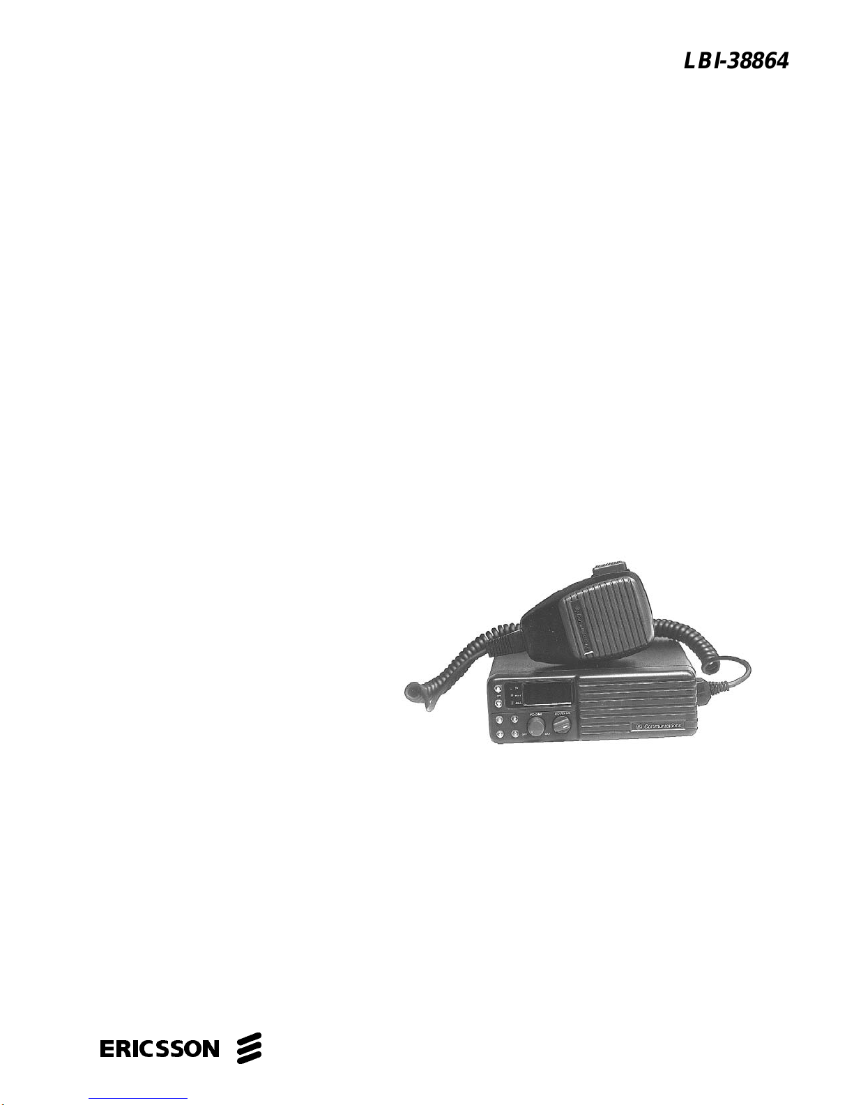
VHF MOBILE RADIO
MODEL MGM 148 & 160
ericssonz

MONOGRAM SERIES LBI-38864B
TABLE OF CONTENTS
TABLE OF CONTENTS
SPECIFICATIONS . . . . . . . . . . . . . . . . . . . . . . . . . . . . . . . . . . . . . . . . . . . . . . . . . . . . . . . . . . . . . . . . . . . . . . . . . 1-4
Receiver (P ER E IA RS-204-C). . . . . . . . . . . . . . . . . . . . . . . . . . . . . . . . . . . . . . . . . . . . . . . . . . . . . . . . . . . 2
Transmitter (PER EI A R S-1 52-B). . . . . . . . . . . . . . . . . . . . . . . . . . . . . . . . . . . . . . . . . . . . . . . . . . . . . . . . . 3
Options And Accessories . . . . . . . . . . . . . . . . . . . . . . . . . . . . . . . . . . . . . . . . . . . . . . . . . . . . . . . . . . . . . . . 4
UNPACKING . . . . . . . . . . . . . . . . . . . . . . . . . . . . . . . . . . . . . . . . . . . . . . . . . . . . . . . . . . . . . . . . . . . . . . . . . . . . . . . 5
GENERAL DESCRIPT I O N . . . . . . . . . . . . . . . . . . . . . . . . . . . . . . . . . . . . . . . . . . . . . . . . . . . . . . . . . . . . . . . . . . . 6
DESCRIPTION OF CONTROLS. . . . . . . . . . . . . . . . . . . . . . . . . . . . . . . . . . . . . . . . . . . . . . . . . . . . . . . . . . . . . . . 7-8
Front Panel Controls . . . . . . . . . . . . . . . . . . . . . . . . . . . . . . . . . . . . . . . . . . . . . . . . . . . . . . . . . . . . . . . . . . 7
Rear Pan el Controls. . . . . . . . . . . . . . . . . . . . . . . . . . . . . . . . . . . . . . . . . . . . . . . . . . . . . . . . . . . . . . . . . . . 8
GENERAL OPERATI O N . . . . . . . . . . . . . . . . . . . . . . . . . . . . . . . . . . . . . . . . . . . . . . . . . . . . . . . . . . . . . . . . . . . . . 9-10
Radio On/off , Powe r U p. . . . . . . . . . . . . . . . . . . . . . . . . . . . . . . . . . . . . . . . . . . . . . . . . . . . . . . . . . . . . . . . 9
Receiving. . . . . . . . . . . . . . . . . . . . . . . . . . . . . . . . . . . . . . . . . . . . . . . . . . . . . . . . . . . . . . . . . . . . . . . . . . . . 9
Transmitting . . . . . . . . . . . . . . . . . . . . . . . . . . . . . . . . . . . . . . . . . . . . . . . . . . . . . . . . . . . . . . . . . . . . . . . . . 9
Digital Channe l Guar d. . . . . . . . . . . . . . . . . . . . . . . . . . . . . . . . . . . . . . . . . . . . . . . . . . . . . . . . . . . . . . . . . 10
CIRCUIT ANALYSI S . . . . . . . . . . . . . . . . . . . . . . . . . . . . . . . . . . . . . . . . . . . . . . . . . . . . . . . . . . . . . . . . . . . . . . . . 11-13
Receiver. . . . . . . . . . . . . . . . . . . . . . . . . . . . . . . . . . . . . . . . . . . . . . . . . . . . . . . . . . . . . . . . . . . . . . . . . . . . . 11
Transmitter . . . . . . . . . . . . . . . . . . . . . . . . . . . . . . . . . . . . . . . . . . . . . . . . . . . . . . . . . . . . . . . . . . . . . . . . . . 12
Frequenc y Synthe size r . . . . . . . . . . . . . . . . . . . . . . . . . . . . . . . . . . . . . . . . . . . . . . . . . . . . . . . . . . . . . . . . . 12
PREVENTIVE MAINTENANCE. . . . . . . . . . . . . . . . . . . . . . . . . . . . . . . . . . . . . . . . . . . . . . . . . . . . . . . . . . . . . . . 14
Connections . . . . . . . . . . . . . . . . . . . . . . . . . . . . . . . . . . . . . . . . . . . . . . . . . . . . . . . . . . . . . . . . . . . . . . . . . 14
Electrical System. . . . . . . . . . . . . . . . . . . . . . . . . . . . . . . . . . . . . . . . . . . . . . . . . . . . . . . . . . . . . . . . . . . . . . 14
Mechanical Inspection . . . . . . . . . . . . . . . . . . . . . . . . . . . . . . . . . . . . . . . . . . . . . . . . . . . . . . . . . . . . . . . . . 14
Antenna . . . . . . . . . . . . . . . . . . . . . . . . . . . . . . . . . . . . . . . . . . . . . . . . . . . . . . . . . . . . . . . . . . . . . . . . . . . . . 14
Alignment . . . . . . . . . . . . . . . . . . . . . . . . . . . . . . . . . . . . . . . . . . . . . . . . . . . . . . . . . . . . . . . . . . . . . . . . . . . 14
Frequency Check . . . . . . . . . . . . . . . . . . . . . . . . . . . . . . . . . . . . . . . . . . . . . . . . . . . . . . . . . . . . . . . . . . . . . 14
DISASSEMBLY . . . . . . . . . . . . . . . . . . . . . . . . . . . . . . . . . . . . . . . . . . . . . . . . . . . . . . . . . . . . . . . . . . . . . . . . . . . . . 15-16
Top And Bottom Co ve r s . . . . . . . . . . . . . . . . . . . . . . . . . . . . . . . . . . . . . . . . . . . . . . . . . . . . . . . . . . . . . . . . 15
Front Panel. . . . . . . . . . . . . . . . . . . . . . . . . . . . . . . . . . . . . . . . . . . . . . . . . . . . . . . . . . . . . . . . . . . . . . . . . . 15
RF Board. . . . . . . . . . . . . . . . . . . . . . . . . . . . . . . . . . . . . . . . . . . . . . . . . . . . . . . . . . . . . . . . . . . . . . . . . . . . 15
Digital Board . . . . . . . . . . . . . . . . . . . . . . . . . . . . . . . . . . . . . . . . . . . . . . . . . . . . . . . . . . . . . . . . . . . . . . . . 16
PROGRAMMING INSTRUCT IONS . . . . . . . . . . . . . . . . . . . . . . . . . . . . . . . . . . . . . . . . . . . . . . . . . . . . . . . . . . . . 17
TEST EQUIPMENT SETUP . . . . . . . . . . . . . . . . . . . . . . . . . . . . . . . . . . . . . . . . . . . . . . . . . . . . . . . . . . . . . . . . . . 18
ALIGNMENT PROCEDURE. . . . . . . . . . . . . . . . . . . . . . . . . . . . . . . . . . . . . . . . . . . . . . . . . . . . . . . . . . . . . . . . . . 19-23
Page -i-
Oct. 94

MONOGRAM SERIES LBI-38864B
TABLE OF CONTENTS
Suggested Tes t Equi pment . . . . . . . . . . . . . . . . . . . . . . . . . . . . . . . . . . . . . . . . . . . . . . . . . . . . . . . . . . . . . . 19
Pre-A lignm ent Notes :. . . . . . . . . . . . . . . . . . . . . . . . . . . . . . . . . . . . . . . . . . . . . . . . . . . . . . . . . . . . . . . . . . 19
Programming For Alignme nt. . . . . . . . . . . . . . . . . . . . . . . . . . . . . . . . . . . . . . . . . . . . . . . . . . . . . . . . . . . . 19
PLL Alignment . . . . . . . . . . . . . . . . . . . . . . . . . . . . . . . . . . . . . . . . . . . . . . . . . . . . . . . . . . . . . . . . . . . . . . . 20
Transmitter Alignment . . . . . . . . . . . . . . . . . . . . . . . . . . . . . . . . . . . . . . . . . . . . . . . . . . . . . . . . . . . . . . . . . 20
Recei ve r Al ignment. . . . . . . . . . . . . . . . . . . . . . . . . . . . . . . . . . . . . . . . . . . . . . . . . . . . . . . . . . . . . . . . . . . . 22
ALIGNMENT POINTS 406041- F Issue:H DIGITAL BOARD . . . . . . . . . . . . . . . . . . . . . . . . . . . . . . . . . . . . . . 24
ALIGNMENT POINTS 406039- E Issue:H RF BOARD . . . . . . . . . . . . . . . . . . . . . . . . . . . . . . . . . . . . . . . . . . . . 25
PERFORMANCE TEST. . . . . . . . . . . . . . . . . . . . . . . . . . . . . . . . . . . . . . . . . . . . . . . . . . . . . . . . . . . . . . . . . . . . . . 26-28
Transmitter . . . . . . . . . . . . . . . . . . . . . . . . . . . . . . . . . . . . . . . . . . . . . . . . . . . . . . . . . . . . . . . . . . . . . . . . . . 26
Receiver. . . . . . . . . . . . . . . . . . . . . . . . . . . . . . . . . . . . . . . . . . . . . . . . . . . . . . . . . . . . . . . . . . . . . . . . . . . . . 27
COMPONENT REPL ACEME NT . . . . . . . . . . . . . . . . . . . . . . . . . . . . . . . . . . . . . . . . . . . . . . . . . . . . . . . . . . . . . . 29-30
Surface Mount Compone nt Repl aceme nt. . . . . . . . . . . . . . . . . . . . . . . . . . . . . . . . . . . . . . . . . . . . . . . . . . . 30
ELECTRICAL PARTS LIST. . . . . . . . . . . . . . . . . . . . . . . . . . . . . . . . . . . . . . . . . . . . . . . . . . . . . . . . . . . . . . . . . . . 31
PRINTED CIRCUIT BOAR D LAYOUTS . . . . . . . . . . . . . . . . . . . . . . . . . . . . . . . . . . . . . . . . . . . . . . . . . . . . . . . . 32
Top View 406041-F Issue: H / DIGITAL Board . . . . . . . . . . . . . . . . . . . . . . . . . . . . . . . . . . . . . . . . . . . . . 32.1
Bottom View 406041- F Issue: H / DIGITAL Boa rd. . . . . . . . . . . . . . . . . . . . . . . . . . . . . . . . . . . . . . . . . . . 32.2
Top View 406039-E Issue: H / RF Board. . . . . . . . . . . . . . . . . . . . . . . . . . . . . . . . . . . . . . . . . . . . . . . . . . . 32.3
Bottom View 406039-E Issue: H / RF Board. . . . . . . . . . . . . . . . . . . . . . . . . . . . . . . . . . . . . . . . . . . . . . . . 32.4
Misc. Printed Circuit B oards . . . . . . . . . . . . . . . . . . . . . . . . . . . . . . . . . . . . . . . . . . . . . . . . . . . . . . . . . . . . 32.5
Misc. Printed Circuit B oards . . . . . . . . . . . . . . . . . . . . . . . . . . . . . . . . . . . . . . . . . . . . . . . . . . . . . . . . . . . . 32.6
EXPLODED VIEW . . . . . . . . . . . . . . . . . . . . . . . . . . . . . . . . . . . . . . . . . . . . . . . . . . . . . . . . . . . . . . . . . . . . . . . . . . 33
SCHEMATICS. . . . . . . . . . . . . . . . . . . . . . . . . . . . . . . . . . . . . . . . . . . . . . . . . . . . . . . . . . . . . . . . . . . . . . . . . . . . . . 34
Page -ii-
Oct. 94

MONOGRAM SERIES LBI-38864B
SPECIFICATIONS
SPECIFICATIONS
GENERAL
Frequency Range
VHF Low Band 136-150 MHz
VHF Mid Band 148-165 MHz
VHF High Band 160-174 MHz
Channel Capability 16 max
Channel Spacing 25 or 30 kHz
Input V oltag e 13.8 VDC negative gro und
Current Dr ain
Standby 0.4 Amps (max )
Recei ve 0.8 Amp s (m ax)
Transmit 9.5 Amps (max)
Temperature Range
Dimensions 2 x 6 x 8-1/4 i n
Weight 4 lbs, 3 oz
FCC Compliance Parts 15, 22, 74, 90
FCC ID Designation
136-150 MHz N / A
148-165 MHz F3J9QLSM4150
160-174 MHz F3JSM415H
DOC (Canada) Type Appr oval
136-150 MHz N / A
148-165MHz 287194150I
160-174 MHz 287194100I
-30° to +60° C
(51 x 152 x 210 mm)
(1.9 kg) w/m ic
Page -1-
Nov. 94

MONOGRAM SERIES LBI-38864B
RECEIVER (PER EIA RS-204-C)
RF Input Im pedance 50 ohms no mi na l
Sensitivity
EIA 12 dB SINAD 0.30 mV
SPECIFICATIONS
20 dB QUIETING
Squelch Sensitivity 0.25 mV thr esh old
Selectiv ity -70 dB
Inter modula tio n -70 dB
Modulation Acceptanc e Bandwidth
Spurious and Image 70 dB mx
Audio Power Output 5 Watts @ % distortion into 4 ohm load)
Frequency Stability
Operationa l Bandwidth 10 MHz
VHF PROGRAMM ING CHART RECEIVE
Frequenc y Sprea d Band Width Factory Pro gr amm ed Fre q.
136 - 150 MHz 10 MHz 136 - 146 MHz
0.50 µV
± 7.5 kHz
± 0.0005%
(3 dB degradation at band limits)
Spreads
(3 dB Degra da ti on a t lim it s)
148 - 165 MHz 10 MHz 150 - 160 MHz
(3 dB Degra da ti on a t lim it s)
160 - 174 MHz 10 MHz 162 - 172 MHz
(3 dB Degra da ti on a t lim it s)
Page -2-
Nov. 94

MONOGRAM SERIES LBI-38864B
SPECIFICATIONS
TRANSMITTER (PER EIA RS- 152-B)
RF Power O utput 40 W (adju sta bl e)
RF Output Impedance 50 ohms
Spurious and Harmo nics -70 dBc
Modulation 16 K0F3E
FM Hum and Noise -45dB nomina l
Audio Distortion < 3 % @ 1000 Hz
Frequency Stability
Operationa l Bandwidth 10 MHz
VHF PROGRAMM ING CHART TRANSMIT
Frequenc y Sprea d Band Width Factory Pro gr amm ed Fre q.
136 - 150 MHz 10 MHz 136 - 146 MHz
148 - 165 MHz 10 MHz 150 - 160 MHz
160 - 174 MHz 10 MHz 162 - 172 MHz
± 0.0005%
(3 dB degradation at band limits)
Spreads
(3 dB Degra da ti on a t lim it s)
(3 dB Degra da ti on a t lim it s)
(3 dB Degra da ti on a t lim it s)
Page -3-
Nov. 94
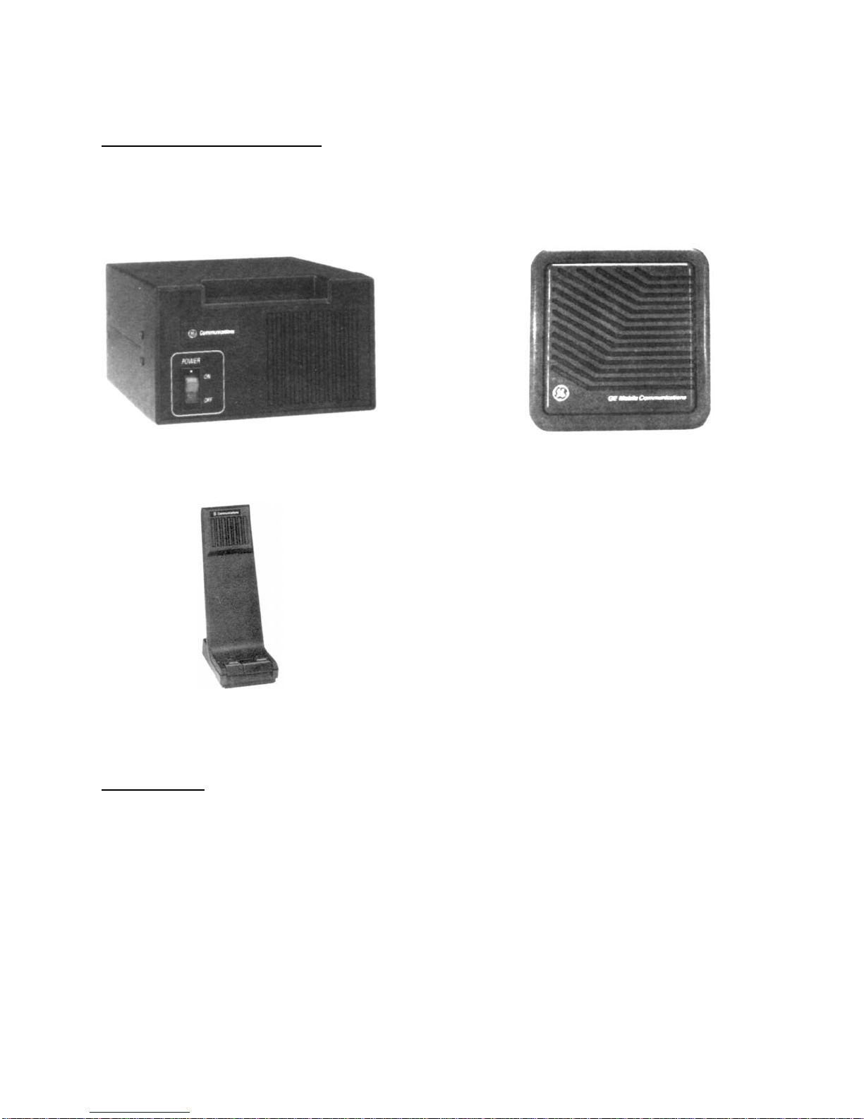
OPTIONS AND AC CESSORIES
CONTROL STATION OPTIONS:
MONOGRAM SERIES LBI-38864B
SPECIFICATIONS
Power Supply MGPS5V
Desk Microphone MGMC5H
NOT SHO WN:
Antenna - MGAN1A
Relay Kit - MGSU1C
External Speaker MGZM7C
Noise Suppressi on K it - MGPD1A
Page -4-
Nov. 94
MONOGRAM SERIES LBI-38864B
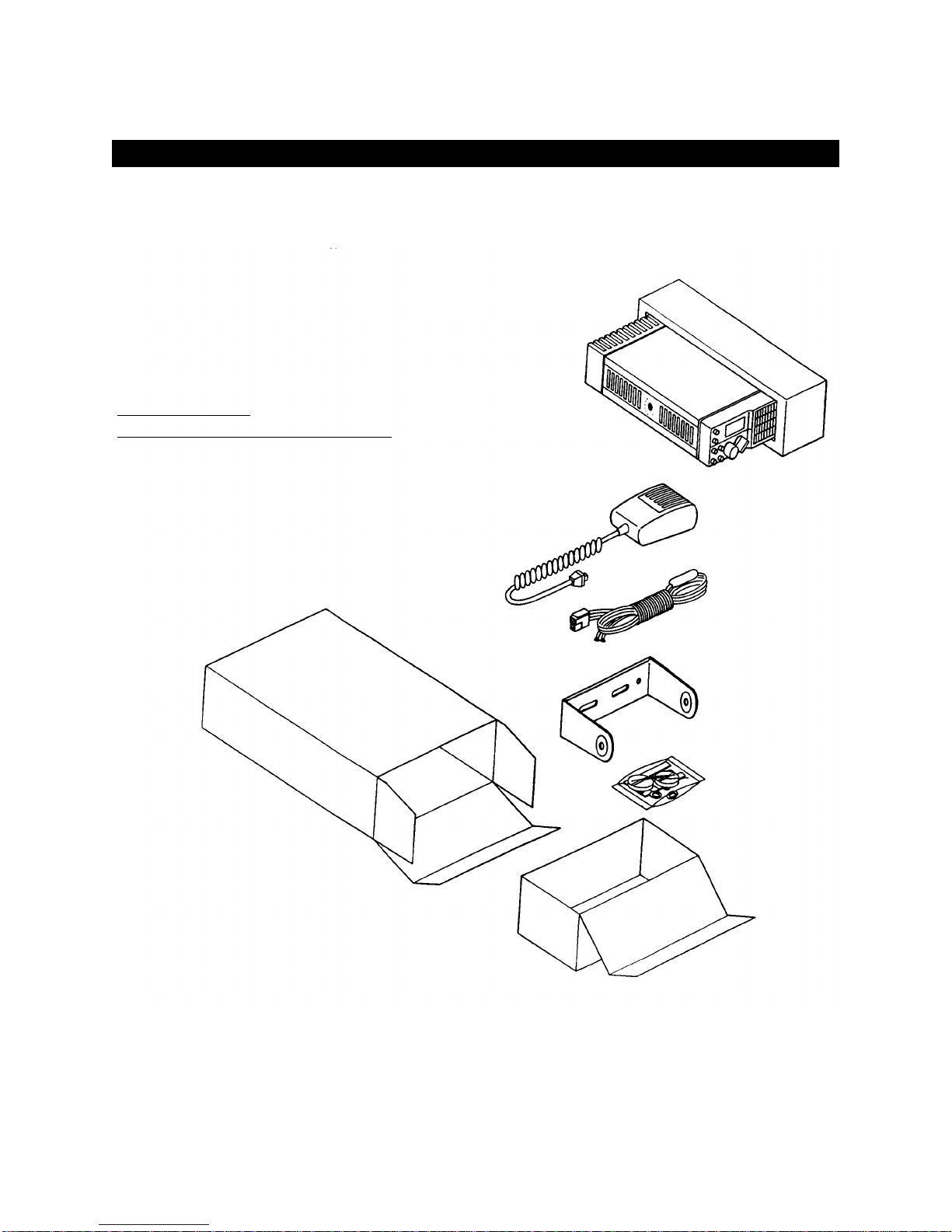
UNPACKING
UNPACKING
Check th e ca rto n an d pa ck ing mate ri a l car ef ully for the followi ng i te m s:
1. Transceive r Uni t
2. Microphon e
3. DC power Cord
4. Mobile Mounting Brac ke t
5. Assembly Hardware
6. Operating Guide
Styrofoam not used
Inner packing is now cardboar d tr ay box.
FIGURE 1 - Unpacking Diagr am
Page -5-
Nov. 94

MONOGRAM SERIES LBI-38864B
GENERAL DESCRIPTION
GENERAL DESCRIPTION
Introduction
The Convent iona l Monogra m Serie s Rad io is a rugge d, two-way FM m obi le radio whic h opera t es in eith er the
148-165 MHz band split or the 160-17 4 MHz band split. The Monogra m is a synthesized ra dio util izin g
microcom pu ter te chno log y to provide reliabl e high-qua l it y simpl ex two-way m obi le com mu nic ati ons. Its transm it ter
output power le vel is 40 watt s ove r the wid e band widt h, wit h an allowable 10 MHz ma ximum rec ei ve ch an nel
sepa ra ti on. The ba sic ra dio pack ag e i nc lud es t he following fea tur es:
Features
Microprocessor Control
∗
Synthesized RF Channel Selection (Fr eque nc y Contr ol)
∗
Vacuum Fluorescent Channel Selec tion Displ ay
∗
Channel Guard (CTCSS) Enclode /De code
∗
Digital Channel Guard (DCS Encode /De code )
∗
Priority Scan
∗
± 5 PPM Frequency Stability
∗
Field Pro gramm abl e with PC
∗
Variable Squelch
∗
Internal 5-watt Spe ake r, with Volume Control
∗
Side Mounted Micropho ne Connec tor
∗
Rear Mounte d Antenna Conne ctor (SO-239)
∗
Rear Power Connections
∗
The small siz e of the Monogra m radio ma ke s it ideal for front mou nting i n conve nt ion al vehic les. The radi o is
operat ed with a simpl e hand-he l d mi croph one in combina ti on wit h the op er atin g co ntr ols de sc ri be d in the foll owi ng
section.
Page -6-
Nov. 94
MONOGRAM SERIES LBI-38864B
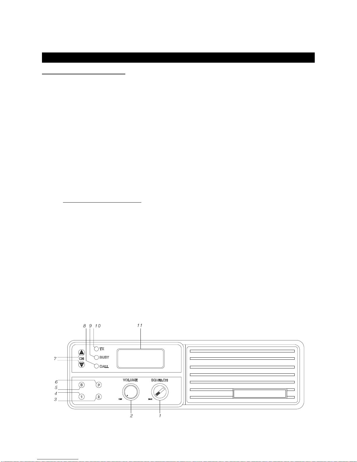
DESCRIPTION OF CONTROLS
DESCRIPTION OF CONTROLS
FRONT PANEL CONTROLS
1. SQUELCH Control: The squelch cont rol will silence the rece iver when no signal is being received .
2. ON/OFF/VOLUME Contr ol: This is the main power swit ch and volume control .
3. Monitor But ton (2): Thi s but ton perform s th re e fu nc tions:
a. Disables tone or digita l squelc h opt ion s when in receive mode .
b. Re tu rns to norma l radi o ope rati on fr om the progra mm ing m ode .
c. Controls di splay intensity.
4. Auxiliary Spe a ker But ton (1): This but ton silenc e s the inte rna l speake r and c onn ect s the auxilia ry speake r
(require s the auxili a ry opt io n pri nte d c ir cu it board to be instal led). It also dele te s channels fr om the scan l ist
while in the programm ing mode .
5. SCAN Push Button (S): This button turns the sc an functi on "ON" (indicat ed by a red backligh t) and "OFF".
It also serves as the ENTER function durin g SCAN progra mmi ng.
6.
PRIORITY SCAN Push Button (P): This button turns the PRIORITY SCAN function "ON" (indicated by a red
backlight) and "OFF". It also provides access to the programming mode when the radio is turned on.
7. Chann el Cha nge but to ns (CH): The cha nne l chang e butt ons all ow the opera t or to scro ll eithe r up or down
through the progra m me d cha nne l s.
8. Call Light Indi c ator (CALL): This gre e n Ligh t E mitt in g Diode (L ED) in dic a to r illum i nate s to indi ca t e
activity on the cha nne l duri ng rec eive whe n code d sque lch or digita l signa l ing options a re used.
9. Busy Channel Indicato r (BUSY): This yell ow Ligh t Emittin g Diode (LED) in dica tor illumi nate s to indicat e
activity on the channel during receive.
10. Transm it LED Indi c ator (T X): Th is re d Ligh t Emi ttin g Diod e (LE D) in dic a tor il lumi na te s duri ng t ransmit
mode. It also wi ll flash to indicat e tha t the synth esi z er is out of lock.
11. Channel Displ ay: The fron t pane l displ ay indic ate d chan ne l numbe r, priority scan numbe rs, pro gra m ming
mode and error m essag es.
FIGURE 2 - Front Panel Control s
Page -7-
Nov. 94
MONOGRAM SERIES LBI-38864B
DESCRIPTION OF CONTROLS
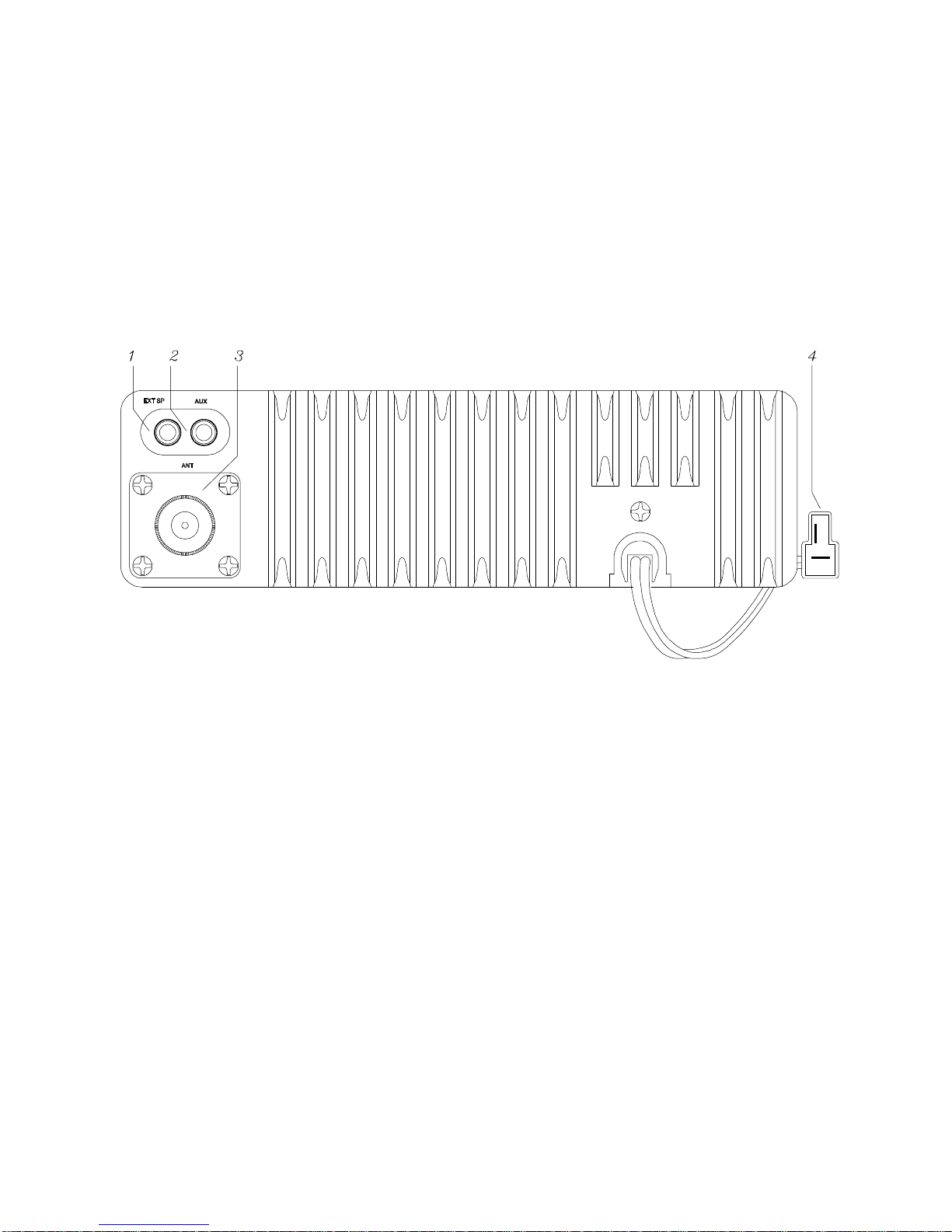
BACK PANEL CONNECTORS
1. Extern al Speak er Conne c to r: Thi s 3.5 mm di ame te r jac k is provi de d for a 4 ohm exte rn al speaker. The
interna l speake r i s sile nc e d whe n the e xt er na l spea ke r is conne c te d.
2. Auxiliary Spea ke r Connect or: This 3.5m m diame ter jack is provide d for an aux iliary spe ake r (Opt ion
MGSU1C Relay Kit is required).
3. Antenna Conne c tor: An SO-2 39 type conne ctor. The output loa d must be 50 ohms.
4. DC 13.8V Connec tor : Polar ize d plug for 13 .8 VDC powe r input- FOR NEGAT IVE GROUND SYST EMS
ONLY.
FIGURE 3 - Back Panel Controls
Page -8-
Nov. 94

MONOGRAM SERIES LBI-38864B
GENERAL OPERATION
GENERAL OPERATION
• NOTE: The foll owi ng desc rip ti on bri e fly o utl ine s the ope rat ion of y our VH F synthesize d mo bile rad io. Consult
the operator’ s manual for a compl ete descri ption of al l the modes of op era tion.
RADIO ON/O FF, POWER UP
1. Turn the rad io on by tur nin g the VOL UME c ont rol one -ha l f tur n cloc kwi se. Aft er "4000" appe a rs in the
display and t he powe r up ale rt tone is gene ra t ed , the displ a y will c ha nge to the #1 priori ty cha nnel. If no
priority chann el has bee n pr ogra m med , the displ a y will cha nge to cha nne l 1.
2. Turn the radio of f by rot a ti ng th e VOL U ME con tro l ful ly cou nte r- cl oc kwi se.
RECEIVING
1. Turn the rad io on and sel ec t the de sire d cha nne l .
2. Depress the MONIT OR but to n (2) if nece ssa ry to illumi na te it’s ba ck light . Adjust the vol um e control to a
comfort able listening level.
3. Rotate the SQUELC H con tro l clockwi se until the sque lch noi se (rushing sou nd) i s no longe r prese nt.
4. Depress the MONIT OR but to n (2) to exti ngui sh the bla ck light.
• NOTE: If the radio is equipped with coded squelch options, depress the MONITOR button (2) to enable the
option; the CAL L indic ato r wil l no longe r be illumi nated.
TRANSMITTING
1. Turn the rad io on and sel ec t the de sire d cha nne l .
2. Pick up the mic roph one and li ste n brie fly to insure the cha nne l is clea r. Alte rna ti ve ly , leave the m icro phone
on-hook and depress the MONITOR button (2).
3. Depress the PT T swi tch on t he side of th e micro phon e. Hold the m icrop hone one to two inch es fr om the
mouth and speak in a normal tone of voice. The TX indicator should be illuminated.
4. Release the PTT switch whe n the message is c om pleted.
Page -9-
Nov. 94

MONOGRAM SERIES LBI-38864B
GENERAL OPERATION
DIGITAL CHAN NEL GUARD
Channel Gua rd pro vid es a mea ns of rest ric t ing calls to spe cif ic radio s thro ugh t he use of a CTCSS (Co nti nuo us To ne
Coded Sque lch) or DCS ( Digi tal ly Co ded Sque lc h) . The tone fr eq ue nc ies ra nge from 67 Hz to 250. 3 Hz a nd the re
are 83 programable codes.
Channel Guard to ne freque nc ie s a nd code s ar e sof twa re progra mm abl e. Both to ne freque nc ie s a nd digit a l code s ma y
be mixed on each chann el . The fre qu enci es and codes a re shown i n Table s 1 and 2. A Chann el Num be r displa y that
does not flash, in dica te s th at Cha nne l Guar d is not prog ra mme d. A flashi ng Cha nn el Numbe r ind ic ate s tha t Cha nne l
Guard is progr amm e d and disa bl ed.
Table 1 - Cha nne l Gu ar d To ne Freque ncies
Standard Tone Frequencie s in Hertz
67.0 71.9 74.4 77. 0 79. 7 82. 5 85.4 88.5
91.5 94.8 97.4 100.0 103.5 107.2 110.9 114.8
118.8 123.0 127.3 131.8 136.5 141.3 146.2 151.4
156.7 162.2 167.9 173.8 179.9 186.2 192.8 203.5
210.7 218.1 225.7 233.6 241.8 250.3
Table 2 - Primary DCS Code s
Digital Squelch Codes
023 114 174 266 411 506 703
025 115 205 271 412 516 712
026 116 212 274 413 523 723
031 122 223 306 423 526 731
032 125 225 311 431 532 732
036 131 226 315 432 546 734
043 132 243 325 445 565 743
047 134 244 331 446 606 754
051 143 245 332 452 612
053 145 246 343 454 624
054 152 251 346 455 627
065 155 252 351 462 631
071 156 255 356 464 632
072 162 261 364 465 654
073 165 263 365 466 662
074 172 265 371 503 664
Page -10-
Nov. 94

MONOGRAM SERIES LBI-38864B
CIRCUIT ANALYSIS
CIRCUIT ANALYSIS
RECEIVER
RF Ampl ifier
Incoming sig na ls from the ante nna jack are ro uted bac kwa rds t hrou gh the tra nsm itte r lowpa ss fil ter in PIN diod e
switch D12. In recei ve mode , D12 conduc ts all owi ng a low impeda nc e path throu gh the diode to the re cei ver fron t
end circui tr y. The rec eive r RF a mp lifie r se cti on is c om pri se d of two bandpa ss fil te r sec ti ons se pa ra ted by a n
amplifier ba se d aroun d Q1. These two fi lte rs allo w signa l s at or near the ope ra ting fr eq ue nc y to pass but prov ide
strong rejec t ion of the mixer’ s spurious response fr eq ue nc ies. The fi rst fi lte r sect ion is a two pol e desi gn forme d
around RF transformers T1, T2 and thei r assoc iate d cir cuit ry. This filt er is followe d by the RF ampl ifie r tran sist or
Q1. This device is a dual-gate MOSFET which, with its lo w n oise figure, yie l ds good receiver sensitivity while
showing strong resista nc e to over load fr om strong sign al s. The output of Q1 dri ve s a thre e-pol e filte r sect io n forme d
around T3, T4 a nd T 5. The output of the RF ampli fi er sta ge is route d to the first mixe r.
First Mixe r and F irst IF Amplifier
The action of the fir st m ixe r tra nsist or Q2 i s to conve rt incom i ng sig na ls a t the oper at in g frequency to the fre qu en cy
of the first IF whic h is 21. 4 MHz. The outp ut of the mixe r is at a fre que nc y whic h is e qua l to the diffe re nc e betwe en
the freq ue nc y of th e inc om ing signal and the loc a l osci ll at or. In this radio, the lo ca l osci lla tor signa l is ch ose n to be
21.4 MHz below t he ope ra ti ng fre qu ency. The de vic e chosen to perform the mixi ng op er at io n is Q2, a high
performance JFET. T he incomin g signal is appl ie d to the gate of Q2, and the lo ca l oscillator si gnal is filtere d by
transforme rs T6, T7 and associa ted circuit ry befo re being supplie d to the drain of Q2. The dif fere nce fr eque nc y
signal at 21.4 MHz exit s the mixe r at the sou rce of Q2 drives t he first IF filte r XF1 and XF2. XF1 and XF2 for m a
4-pole monol ithi c cryst a l filter pair whi ch in part dete rm ine s the se lec tivi ty of the radio . The output of the crystal
filter is route d to the first IF ampl if ie r for med a rou nd Q3. RF tra nsforme r T8 and T9 provi de proper ma tchi ng of t he
crystal filte rs to insu re good pass ba nd re spo nse and select ivity .
Second Mixer, Second IF, and FM Detector
The output of Q3 is appli e d to the inpu t (pin 16) of IC2. IC2 is a singl e conv er sion FM rece ive r on one integ rate d
circuit chi p. The sig na l at the input is rou ted str aight to a mixe r which con verts t he incom in g signal to the sec ond IF
frequen cy of 455 kHz. Th e sec ond l ocal oscil lato r is for med wi th cryst a l X1 and c ircui tr y wit hin IC2. The output of
the second mix er is at pin 23 which i s con nect e d to a ceram ic ba ndp ass fi lte r CF1 and c en tere d at 455 kHz. This
filter, along wit h XF1 and XF2, determ in e the adja cent chan ne l sele cti vity of the radio. T he outp ut of CF1 dri ves a
high gain IF amplifier chain internal to IC2 which in turn drives the quadrature detector. The output of the detector is
amplified and exits IC2 at pin 9.
Audio
Detecte d audi o from IC2 passe s th roug h a lowpass fil ter fo rm ed around L 7, C53 and C5 2 whic h rem ove s IF
frequen cy compo ne nts a t 455 kHz . The audio signa l then pa ss e s thro ugh bu ffe r amp li fie r tra nsist or Q6 befo re being
filtered by a two sect ion , 4-pol e high pa ss filt er (IC3) This filte r rem ove s DCS and CT CSS lo w freque nc y tone s
from the recov er ed aud io. T ransist ors Q7 a nd Q8 a ct as switc he s around volume cont rol VR2 to mute the au dio
during squelched receive operation. The audio signal is finally routed to audio power amplifier IC5 and then to the
speaker.
Page -11-
Nov. 94

MONOGRAM SERIES LBI-38864B
CIRCUIT ANALYSIS
Squelch
The presence of an RF carrier is determined by noting the level of ultrasonic noise at the detector output (pin 9) of
IC2. When a carri e r is pre se nt , the noise leve l drops. The aud io at pin 9 of IC2 is fi lt ered by a two-po le bandpa s s
filter form e d around L5, L 6 C48 and C5 0. This fil ter pa sses at and near an audi o fre qu en cy of 50 kHz. This
frequen cy is high enough that vo ice audio and i ts harm oni c s will not cause impro pe r sque lch op er atio n. The output
of the filter is ro ute d to an ampl ifie r inte rna l to IC2. The outp ut of the ampl if ier dri ve s the squel ch dete ct or D7 an d
D8. The DC voltage at the dete ctor ou tpu t is amplifi ed and filte red by Q4. T he outp ut of Q4 send s its squel ch sign al
to the microprocesso r. When the micropro cessor determ ines th at a valid carrier exists, it sends an unm ute signa l to
the audio switc h transi sto rs Q7 and Q8.
TRANSMITTER
Audio
The micropho ne audio i s ampl ifie d, pre-e mp ha siz ed an d peak limi ted by cir cu it s within IC 113. The output of the
limiter is rout ed thr ough RV4, the mic roph one ; devi ati on c ont rol . Input CTCSS an d routed DCS signa l s are rou te d
through RV5, the CTCSS/ DCS de via tion con tro l. Both sign als ar e summ e d and lowp ass filt e red to remove hi gh
frequen cy compo ne nts fr om the limite r whic h co uld cause chan ne l splatte r. Whe n the mic rop roc essor e na ble s the TX
8 Volt supply, analog gate IC115 deliver s the modul atio n sign al to the VCO transi stor Q112.
RF Driver and Power Amplifi er
Diode D9 acts as a switch all owin g the RF signa l from the phase l ocke d loo p freque nc y syn thesi ze r to pass thro ugh
to the RF driver and powe r amp li fier du rin g re cei ve . Buffe r amp lifie r Q9 am pli fi es the carri e r to the leve l nee ded by
the driver am pli fi er stage s. T he dri ve r am plifiers, of whi ch the last 2 s t ag es a re gain controlled by the au tom a ti c
power control , driv e the fina l ampl ifi er sta ge forme d around Q12. The fina l ampli fi er boost s the carr ier leve l to the
power level set by the aut om atic power c ont rol . The c arrie r si gna l passe s thr ough the autom a tic powe r contr ol
directio na l coupl e r, the RF output lowpass filt er, and t he n is rou ted to the an tenna connector.
Automatic Power Control
The autom ati c power con tro l dire ct io na l coupl e r sampl e s a porti on of t he forward RF power output t o dete rm in e the
RF level. Diode D10 rec ti fies th is RF sa mp le an d produc es a DC vol tage which i s propo rtional to the RF output
level. This DC signal is summe d wi th the voltage set from the powe r ou tpu t cont rol RV2. This vol tage is com pa red
with a volta ge der ive d fr om the TX 8 Volt supply and the dif fe re nc e is am pl ified by IC4. The out put is furt he r
amplified by Q14 and Q13. Th e outpu t volta ge on Q13 is the supply voltag e for the RF dri ve r stage . The outpu t of
the RF driver is propo rtional to its supply volta ge . Th is com ple t es a ne gati ve feedb ac k loop whi c h result s in const a nt
output power ove r sup ply volta ge and temp er ature va riat io ns.
FREQUENCY S YNTHESIZER
The phase loc ked loo p (PLL) freque nc y synt he siz er se ctio n is respon sibl e for genera ting t he RF signa l at the carr ier
frequen cy duri ng tran smit and at the loc al osc illa t or fre qu en cy for the re ce ive r during receive . A PL L func ti ons by
comparing the output frequency of a voltage controlled osc illat or (VCO) with a fixed frequency refere nce . An error
signal is ge ne ra t ed whic h dri ve s the c ont rol inpu t of the volt a ge con tro ll ed osci ll ator to force its fre que ncy to match
the refere nce. The PLL ba se d fre qu ency synth esi z er has a digit al fre que nc y di vi de r inse rted betwe e n the out put of
the VCO and the freque ncy c ompa riso n circ ui try . As this divid er numbe r is varied , the outp ut freq ue ncy of the VCO
varies a s well with a frequency step size e qua l to the re fe rence fre que nc y ( 5 kHz i n thi s ra dio ). This allows a larg e
range of freq ue ncie s to be gene ra ted wi th on e well co ntr olle d osc illa to r signal , the refe renc e.
PLL Integrated circ uit
IC108 cont ai ns most of the digital circ ui try to form a PLL frequ ency synth esi z er . Thi s inc lu de s a refe rence oscill a tor ,
program ma bl e varia bl e fr eq ue nc y div ider, a mod ulu s con tro l c ount e r, a phase /f re que ncy compa ra tor and a frequ en cy
lock dector. Th e oper atio n of this integrated circ uit is cont rol led by the radio’ s mi cropro ce ssor through a seria l data
line.
Page -12-
Nov. 94

MONOGRAM SERIES LBI-38864B
CIRCUIT ANALYSIS
Reference Oscillator
Crystal X3, va rac tor diod e D119, a thermi sto r/r esi sto r network and oscilla to r stage of IC108 fro m a tem pe ratur e
compe nsa te d 10. 24 MHz osc illa t or. Th is fre qu ency is divided by 2084 to ge ne rate the 5 kHz re fe rence frequenc y for
the PLL freque nc y synt hesizer. This re fe renc e dete rmine s th e freq ue nc y stabi li ty of the ove ra ll radio .
V oltage Controlled Oscillator
FET transistor Q112 and its associ ate d circui try form a ground ed gate oscilla tor which is voltag e tuned by varac tor
diodes D120 and D12 1 and whic h is ban dswit che d by diode s D122 a nd D123 (D126 and D127 for Low band ). The
VCO output is buffere d and isol ate d by Q113, Q114 and Q119 . Audio modula tion is app lied to the source of Q112
to produce frequency modulation during transmit.
Dual Modulus P rescaler
The inter na l di vid er s within IC108 are not abl e to ope ra t e at the VCO o utp ut fr eq ue nc y. To all e via t e this pr obl em ,
part of the ove ra l l fre quency divi s io n ne ce s sary bet wee n t he VC O and the pha se /frequency comp arator is pla c ed
external to, and cont rol le d by, IC1 08. IC10 9 div ides th e VCO freq ue nc y by 64 or 65, dete rm ined by the sta te of
IC108 pin 6. This prod uc es a lowe r freq ue nc y whic h ca n be furthe r div ide d by IC108. By strate gi c timing whe n to
divide by 64 or 65, the overall division will be that nec essar y to put the VCO on the corre ct frequ en cy.
Loop Filter
Resistors R3 16, R323, R3 24, R325, R326 a nd c ap aci tor s C263, C26 4 and C265 form the lo op fi lter . The purpose of
the loop filte r is to filter out the 5 kHz refe re nc e freq ue nc y prod ucts from the output of phase/frequ en cy compa ra tor
IC108 and to determine the dynamic operation of the overall loop.
R315, C262, Q107 and Q108 act to spee d up oper atio n of the synthesizer loop durin g ch anne l cha nge s and duri ng
frequ en cy tra n si ti on (rece ive to tran sm it and tra nsmit to receive) .
Out-Of-Lock Detector
IC108 cont ai ns a circ uit whic h com pa res the tim ing diff er en ce of the 5 kHz refere nc e fre que nc y a nd t he divi de d
down VCO frequenc y. The outpu t is a 5 kHz pulse whose dur atio n is equa l to the timing diff eren ce . R312 and C295
filter this pulse and ave rage it produc i ng a DC volta ge which is pr opor ti ona l to the pul se widt h. When the loop is in
lock, this vo lt ag e is zero, but when the lo op is i n lock, th is vol tage is z e ro, but when the loop is out of lock , it ri ses to
a level which will forward bia s Q106. The output of Q106 dri ve s the mic rop roc e ssor. The mic ro proc e ssor will not
allow the radi o to t ra ns m it unle s s th e sy n thesize r i s in lock. This is to pr ev en t out of ba nd signals from bei ng
transmi tt e d.
Page -13-
Nov. 94

MONOGRAM SERIES LBI-38864B
PREVENTIVE MAINTENANCE
PREVENTIVE MAINTENANCE
To ensure hig h opera ti ng effi c ienc y and to preve nt me ch an ica l and ele ctri c al fail ure s from inte rru pti ng syste m
operation s, ro uti ng che c ks shoul d be made of all mec ha ni cal and elec tric a l part s at regular interva ls. Pre venti ve
maintenance shou ld include the followi ng checks:
CONNECTIONS
Ground connec tions t o the volta ge source should be peri odi cal ly che c ked for t igh tness. Loose or poor con ne ctio ns to
the power so urce will ca use excessive volta ge drops and f au lty operati on. When ground conne ctions are not made
directly to the bat tery, the connec t ion from the batt ery to veh icle cha ssis m ust be che ck ed for low im pe da nc e. A hig h
impedance may ca use exce ssiv e voltag e drops a nd alt erna tor noise proble ms.
ELECTRICAL SYSTEM
Check the volt ag e regu lato r an d altern at or or gen er ator pe riodically to keep the ele c tric al syste m within safe and
econom ica l op er atio n li mi ts. Over vol ta ge is indicated when the batt er y lose s wa te r rapi dly. Usage of 1 or 2 ounc es
of water per ce ll per wee k is ac ce pta ble for batteri e s in cont inu ous operation . A we ak batter y will oft en cause
excessive noi se or faulty ope ra tion.
MECHANICAL I NSPECTION
Since mobi le uni ts a re subjec t to co nsta nt shock a nd vi bra tion, check for loose plug s, nu ts, scr ews and ot he r pa rt s to
make sur e tha t not hi ng is w or kin g loo se.
ANTENNA
The antenna , ante nna base and a ll co ntac ts sho uld be kept cle an and fre e from corrosi on. If the ant en na or its base
should become coated or poorly ground ed, loss of radi ation and a wea k signal will resul t.
ALIGNMENT
The transmit ter a nd rec e iver m ete r rea din gs shoul d be ch ecke d peri odi c al ly, and t he alignment "tou ched up" whe n
necessa ry . Refe r to the Ali gnm e nt Proc ed ure in this Se rvi ce Ma nua l .
FREQUENCY CHECK
Check the tra nsm itte r fre qu ency and devia tion. Norma ll y, these checks are made when th e unit is first put into
operat ion , aft er the fir st six mon ths, and onc e a yea r th er ea ft e r.
Page -14-
Nov. 94

MONOGRAM SERIES LBI-38864B
DISASSEMBLY
DISASSEMBL Y
TOP AND BOTT OM COVERS
There are no screws used to secure the top and bottom covers. Both top and bottom covers are removed
with a flat blade screwdriver or similar tool. On each side of the radio there are two small slots (one at the
top and one at the bottom). Insert the screwdriver into the slot and gently pry the lip of the cover out from
the radio. Without removing the screwdriver from the slot and in the same motion, pry the cover up. Both
covers can be removed from either side of the radio.
FRONT PANEL
1. Remove the (6) M3 x 6 mac hin e sc re w s (3 on t op a nd 3 on bo tt om ) tha t sec ure th e Front Pane l t o the
chassis.
2. Two cable s con ne ct the Contro l Boa rd to the RF Bo ar d (at PL 1) a nd to the Digi ta l Boa rd (a t PL2). These
cables ma y be unplug ged at the RF Board and at the Digital B oard. A ribb on cable from the Display Boar d
is connect ed to th e Digital Board (at FLT) a nd m a y be unplugged to remo ve it.
RF BOA RD
• NOTE: Any reference to item’s in the following disassembly procedure pertain to the Exploded View Parts
Breakdown pa ge.
1. Remove the (13 ) M3 x 24 machine scr ews se curi ng th e RF shie ld to the chassis.
2. Remove the M3 x 8 machine screw tha t secu re the DC Cord brack et to the chassi s. Slide th e bracke t and
cord out of the chas si s.
3. Remove the (6) M3 x 6 mac hin e sc re ws (3 on t op a nd 3 on bo tt om ) tha t sec ure th e Fro nt P a ne l to the
chassis.
4. Remove the RF shield by pushin g the Fron t Pane l forwar d so the shield wil l clear and th en sliding the DC
Cord, bracket and connector through the rectangular hole in the shield.
5. De-solder the ante nn a connec tor fro m the RF Board.
6. Remove the remaining (11) machine screws securing RF Board, IC1, Q11 and Q13.
7. Unplug the VCO cabl e fr om the jack an d remo ve the RF Board
Page -15-
Nov. 94

MONOGRAM SERIES LBI-38864B
DISASSEMBLY
DIGITAL BOARD
1. Rem ove the (6) M3 x 18 machi ne scre ws that secur e the Top Pane l shie ld to the chassis.
2. Unplug and remove the Auxilla ry Rel ay P.C.B. at PL5.
3. Remove the (6) mac hin e scre ws (3 on top and 3 on bottom) that sec ure the Front Pane l to the chassis.
• The following steps detail the removal of the RF shield which is necessary before continuing with the removal
of the Digital Board.
4. Remove the (13 ) M3 x 24 machine scr ews se curi ng th e RF shie ld to the chassis.
5. Remove the M3 x 8 machine screw tha t secu re the DC Cord brack et to the chassi s. Slide th e bracke t and
cord out of the chas si s.
6. Remove the RF shield by pushin g the Fron t Panel for war d so the shield will cle ar and th en sliding the DC
Cord, bracket and connector through the rectangular hole in the shield.
7. Unplug the VCO cabl e from the jack.
8. Remove the rem ai ning (10) screws sec uri ng th e Di gita l Boa rd , IC5, IC6 and IC1 04 to the ch assi s.
9. The Digital Board can now be removed from the chassis, however the Front Panel assembly is still atta c h ed b y
two cables (one from the Control board and one from the Display board). The cable from the Control Board at PL2
may be unpl ugg ed. Th e ri bbon c able fro m Digi tal B oar d ma y be u npl ugge d a t F LT.
Page -16-
Nov. 94

MONOGRAM SERIES LBI-38864B
PROGRAMMING INSTRUCTIONS
PROGRAMMING INSTRUCTIONS
The VHF synthesized mobile radio is equipped with a personality EEPROM. All customer information
such as the customer frequencies, customer tones and customer options are stored in the EEPROM. The
EEPROM contains all information to tailor the operation of the radio to the user’s requirements. The
EEPROM is programmed by using an IBM compatible personal computer with MSDOS, Programming
Cable TQ-3376 and P rogrammi ng softw are TQ-3375 .
PROGRAMMING THE RADIO
The programm in g Cable T Q-337 6 is a Y-cabl e. The base of the "Y" has a standa rd 25 pin connect or whi ch plugs
into the com pu te r, the rem ai ni ng e nd ha s a 6 pin c onne c to r whic h fi ts i nto the co nne c tor PL1 on the digit al boa rd
inside the radio. To use this cable, remove the top cover of the radio as described in the DISAASSEMBLY sect ion.
Plug the 6 pin connector into the socket insid e the radio (PL1) , whic h is located near the EEPROM IC1 07. Plug the
base of the "Y" into the comput e r that will prog ra m the rad io. See the dia gra m in TQ-3375 Soft war e Manua l . In
order to program the radio with the progra mmi ng cab le, it is necessa ry to put the radio into the progra mm ing m ode .
To do this, pre ss the P "Priorit y" but ton /L E D on the radi o an d tur n the radio ON. The radio wi ll sound a prom pt
tone and show the word s "PROG" on the di spla y. Please re fe r to the Soft wa re Manu al for fu rth er instruc ti ons on the
operation of the Prog ra mmi ng Soft wa re. After compl e ting th e progra m m ing instruc ti ons in the Ma nua l, re m ove the
cable from PL 1 and repla ce the cove r on your VHF synth esi z ed mob ile radi o.
Page -17-
Nov. 94
MONOGRAM SERIES LBI-38864B
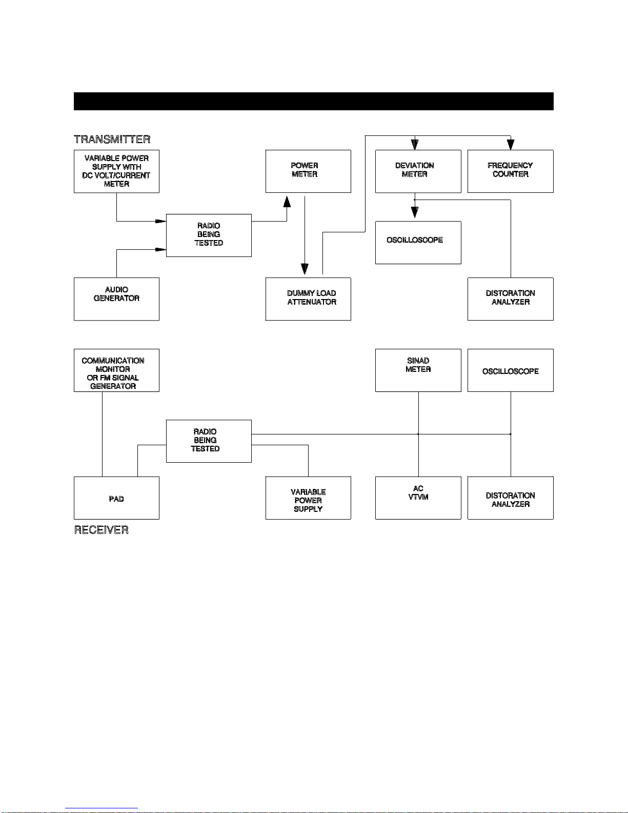
TEST EQUIPMENT SETUP
TEST EQUIPMENT SETUP
*
Figure 4 - Test Equipment Setu p
* Optio na l T est Eq uip me nt
Page -18-
Nov. 94
*

MONOGRAM SERIES LBI-38864B
ALIGNMENT PROCEDURE
ALIGNMENT PROCEDURE
• WARNING: Any repairs or adjustments shoul d be made under the supe rv ision of a certifie d technic ian.
SUGGESTED TEST EQUIPMENT
The following equipm ent, or its equival ent, is requ ired for prop er align ment of your VHF synthesi z ed mobil e radio:
1. Termal ine W att me te r, or T hrou gh-l in e Wa tt mete r wi th ter mina ti on i nto 50 ohm dum m y load.
2.
AC/DC VOM with a minimum of 1 MΩ input impedance.
3. SINAD Meter.
4. FM Communications Monitor.
5. Regulated Power Supply capa ble of 9 volts to 16 volts adjustable; at least 10 ampere capab ility.
6. Oscillosc op e.
7. Audio Distortio n Met er (de sir ab le but not nece ssar y).
8. Frequenc y Co unt er .
PRE-ALIGNMENT NOTES:
1. Refer to the Ali gnm e nt Point s Drawings as requi re d for l ocat io n of com pone nt s.
2. The VHF synthe si ze d mobi le radi o cove rs the fol lo wing freque nc y ra nge s, 148- 165 MHz ba nd a nd
160-174 MHz band, without compone nt change s.
3. The radio has be e n fact ory align ed for ope ra t ion with in the cent er 10 MHz porti on of eac h of the band s. If
operat ion is to be withi n thi s ra nge , no furthe r a lignm e nt i s nece s sa ry. If ope ra t ion outsi de this ra nge (but
still wit hin the appropriate frequency band) is desired, the following al ignment procedure should be
performed .
PROGRAMMING FOR ALIGNMENT
For the alignme nt proc e dur es the EEPROM shou ld be progra m med as fol lows:
1. An EEPROM shoul d be progr amm ed wit h 3 transm it and 3 rec eive freque nc i es.
2. The lowest and highest frequenc ies shou ld enclose t he user ’s freque nci es and be 8 MHz apart. The lowest
and highest fr eq ue nc ies mu st be wit hin the appropriate fr eque nc y ba nd.
3. In addition t o progra mm i ng fre qu en cie s, CTCSS a nd DCS c ode s must a lso be progra m m ed to insure that
the modulation de via ti on for these potent ial options i s corre ct , even if they a re not to be used for the
customer’ s ope ra tion. Th e foll owin g forma t sho uld be used:
Lowest RX/TX fre quenc y 67.0 Hz CTCSS Tone
Middle RX/TX fre qu en cy DCS Code 072
Highest RX/T X freque ncy 250.3 HzCTCSS Tone
Highest RX/TX frequency No Tone Options
Page -19-
Nov. 94

MONOGRAM SERIES LBI-38864B
ALIGNMENT PROCEDURE
4. The middle RX/TX frequencies should be halfway between the lowest and the highest frequencies.
• NOTE: There shoul d be 4 channels programm ed with a total of 3 different freque ncie s.
PLL ALIGNMENT
1. Connect an RF dum my loa d or power attenua tor (50 watt mini m um ratin g) to the an te nna conne c to r.
2. Connect a VOM or DVM to TP1, accessed through a hole in the VCO cover.
3. Set the CHANNEL selector to the highest transmit frequency.
4. Press the push-to -tal k (PT T) switc h. Adj ust T C5 for a 7.0 VDC readi ng on the VOM. Rele ase the PTT
switch.
5. Change the CHANNEL sele ctor to the lowest transmi t freque nc y.
6.
Press the PTT switch. The VOM should read 1.5 VDC ± 0.2V VDC. If not, re-adj ust TC5 slightl y for a 1.5
VDC reading. Rele ase the PT T switc h.
7. Return to the highest transmit channel and verify that the TP1 voltage does not exceed 8 volts in transmit.
On the lowest transmit freq uency, the vol ta ge mu st be 1. 5 ± 0.2 VDC, and on the highe st tra nsm it
frequency , the voltage must be less tha n 7.5 VDC. Re peat steps 3 throug h 6 if necessar y.
8. Set the CHANNEL selector to the lowest receive frequency.
9. Adjust TC3 to obtain a 2 VDC reading on the VOM.
10. Change the CHANNEL sele ctor to the highest receiv e freq ue ncy. Verify tha t the DC voltag e does not
exceed 7.0 VDC. If it does, re-a dju st T C3 for a 7.0 VDC rea din g.
11. The foll owi ng c ha rt sho ws typical vol tages at TP1:
TP1 VOLTAGE
CHANNEL
Lowest Freque nc y 1.5 VDC 2.0 VDC
Highe st Fr eq uency 7.5 VDC 7. 0 VD C
TRANSMIT RECEIVE
TRANSMITTER
TRANSMITTER ALIGNM ENT
1. Connect a 50 ohm RF dummy load or a powe r att enua tor (50 wa tt minim um rati ng) through a watt me te r
(50 watt scal e ) to the ante nna co nne c tor .
2. Turn RV2 (Automat ic Power Adju stm ent) fully c lockwi se .
3. Connect varia ble DC power suppl y (10 Ampere cap abil ity) to the DC power cab le on the radi o. Set the
voltage to 12 VDC measure d a t the rad io durin g transm i t. (Volta ge drops in the power cabl e durin g transm i t
will lowe r the voltage at the ra di o).
4. Set the CHANNEL sele ctor to a mid-fre qu en cy transm it channe l.
5. Press the PTT swi tch.
6. Adjust RV2 for 40 watt s, or the desired power out put (10 - 40 wa tts). Re lea se t he PTT swit ch .
Page -20-
Nov. 94
 Loading...