

Page 1

Technical Description EN/LZB 119 2506 R1A
Chapter 2
Technical Description
Ericsson Cellular Phone AF738
AF778
i
Page 2

EN/LZB 119 2506 R1A Technical Description
SUBJECT .................................................................................... PAGE
General ................................................................................................................... 2-1
Mechanical........................................................................................................2-2
Table 2-1. Phone Dimensions ............................................................................2-2
Keypad..............................................................................................................2-3
Figure 2-1.Keypad.............................................................................................2-3
Side Volume Keys.............................................................................................2-4
Figure 2-2. Side Volume Keys...........................................................................2-4
LCD..................................................................................................................2-4
Figure 2-3. LCD Display ...................................................................................2-4
Table 2-2. LCD Display Areas...........................................................................2-4
Top Indicator.....................................................................................................2-5
Table 2-3. Top Indicator Functions....................................................................2-5
Vibrator Motor (AF778 Only)............................................................................2-6
Retractable Antenna ..........................................................................................2-6
1/4 Wave Antenna Operation.........................................................................2-6
Figure 2-4. AF778 1/4 Wave Antenna Connections............................................2-7
1/2 Wave Antenna Operation (AF778)...........................................................2-7
Figure 2-5.1/2 Wave Antenna Connections........................................................2-8
Transceiver PCB and Component Layout............................................................. 2-9
Major Components................................................................................................2-10
Figure 2-6. PCB Component Layout................................................................2-10
Table 2-4. Component Table............................................................................ 2-11
Figure 2-7. Block Diagram ..............................................................................2-13
Radio Section.........................................................................................................2-15
General............................................................................................................ 2-15
Table 2-5. Frequencies..................................................................................... 2-15
Duplexer..........................................................................................................2-16
Receiver..........................................................................................................2-16
Receive Front End .......................................................................................2-17
IF Section.................................................................................................... 2-17
Synthesizer......................................................................................................2-18
VCTCXO.................................................................................................... 2-18
BERTINDY.................................................................................................2-19
RX (Main) Synthesizer ................................................................................2-19
TX (Auxiliary) Synthesizer..........................................................................2-20
MALIN .......................................................................................................2-20
Transmitter......................................................................................................2-20
Power Amplifier.......................................................................................... 2-20
ii
Page 3

Technical Description EN/LZB 119 2506 R1A
SUBJECT......................................................................................................... PAGE
Logic Section......................................................................................................... 2-21
Processor/Control Interface............................................................................. 2-21
GUSTAV.................................................................................................... 2-22
6303 Microprocessor................................................................................... 2-22
ROM .......................................................................................................... 2-22
RAM .......................................................................................................... 2-22
Bus Interface............................................................................................... 2-22
Decoder...................................................................................................... 2-22
Serial Interface ............................................................................................ 2-22
External Ports ............................................................................................. 2-22
Watchdog On/Off........................................................................................ 2-23
Beep, Alarm, Ring (BAR)........................................................................... 2-23
Clock Generator .......................................................................................... 2-23
Silent Ring (AF778 Only)........................................................................... 2-23
Internal Ports .............................................................................................. 2-23
Modem ....................................................................................................... 2-24
Baudclock................................................................................................... 2-24
Memories........................................................................................................ 2-24
RAM .......................................................................................................... 2-24
ROM .......................................................................................................... 2-24
EPROM (Flash).......................................................................................... 2-25
EEPROM.................................................................................................... 2-25
User Interface ................................................................................................. 2-26
LCD ........................................................................................................... 2-26
Keyboard.................................................................................................... 2-26
Buzzer ........................................................................................................ 2-26
Illumination ................................................................................................ 2-27
Vibrator Motor (AF778 Only)..................................................................... 2-27
Audio (Baseband) Section............................................................................... 2-27
Receive Audio ............................................................................................ 2-27
Transmit Audio........................................................................................... 2-27
Power Supplies............................................................................................... 2-28
Regulators................................................................................................... 2-28
Reset........................................................................................................... 2-28
On/Off Control............................................................................................ 2-28
Transient/ESD Protection............................................................................ 2-29
Charging Circuit............................................................................................. 2-29
Rapid Charging........................................................................................... 2-30
Figure 2-8. Rapid Charging ............................................................................. 2-30
Trickle Charging......................................................................................... 2-30
Connections On The Transceiver Board.............................................................. 2-31
Antenna Connector......................................................................................... 2-31
iii
Page 4

EN/LZB 119 2506 R1A Technical Description
SUBJECT.......................................................................................................... PAGE
Battery Contacts.............................................................................................. 2-31
Speaker Connector...........................................................................................2-31
LCD Contacts.................................................................................................. 2-31
Microphone Connector....................................................................................2-31
Vibrator Connector (AF778 Only) ...................................................................2-31
Antenna Ground Strap (AF778 Only)...............................................................2-31
System Connector............................................................................................2-32
Figure 2-9. System Connector.......................................................................... 2-32
Table 2-6. System Connector Signals ...............................................................2-32
Specifications.........................................................................................................2-33
iv
Page 5
Technical Description EN/LZB 119 2506 R1A
AF778
END PWR
General
The Ericsson AF738 and AF778 cellular telephones are small, lightweight phones
operating at 4.8v, powered by a 4-cell Nickel Metal Hydride (NiMH) battery. They
are class III cellular telephones for use with the AMPS cellular network.
Features of the phone include:
• Compact and lightweight
• Retractable Antenna
• Power-on greeting
• Multilingual with Language menus
• Built-in charging circuitry
• Authentication capable (system dependent)
• Caller line ID* (CLI)
• Voice mail message waiting indicator* (MWI)
• Negative SID Navigation
• Multiple NAMS (up to four)
• Multiple memory locations:
• Standard memory
• Last 10 Numbers dialed
• 1 Last 0 Caller Line IDs (CLI)
∗
• 5 Scratch Pad Memory Locations
• 5 Secure Memory Locations
• Dual-tone multi-frequency (DTMF) dialing
• RSSI and battery capacity indicators
• Ability to connect to external handsfree equipment
• Meets FCC Hearing Aid Compatibility Standards
• Electronic Lock/Call Restrictions
• Ring tone and volume selection
• System selection
• Different answering methods
• Microphone volume selection
• Auto retry on system busy
• Backlight selection
• Minute Minder Selection
• Auto area code
• Emergency numbers
SEND
∗
Requires software version R5A or higher
2-1
Page 6

EN/LZB 119 2506 R1A Technical Description
• Call time counters
• Silent call alert with vibrator (AF778 only)
• ½ wave up, ¼ wave down antenna
Mechanical
Refer to Table 2-1 for phone dimensions. The telephone consists of:
• A transceiver
• A removable battery
• A removable, retractable antenna
• A removable, active flip
Table 2-1. Phone Dimensions
English Metric
AF738 AF778 AF738 AF778
Length 4.17 in. 4.17 in. 106 mm 106 mm
Width 1.97 in. 1.97 in. 50 mm 50 mm
Thickness .94 in. .94 in. 24 mm 24 mm
Weight
(w/battery)
4.8 oz. 4.9 oz. 137 g 139 g
2-2
Page 7
Technical Description EN/LZB 119 2506 R1A
The transceiver consist of:
• Front cover (with speaker)
• Back cover
• Keypad
• Printed circuit board (PCB)
• LCD/lightguide assembly
• Vibrator (AF778 only)
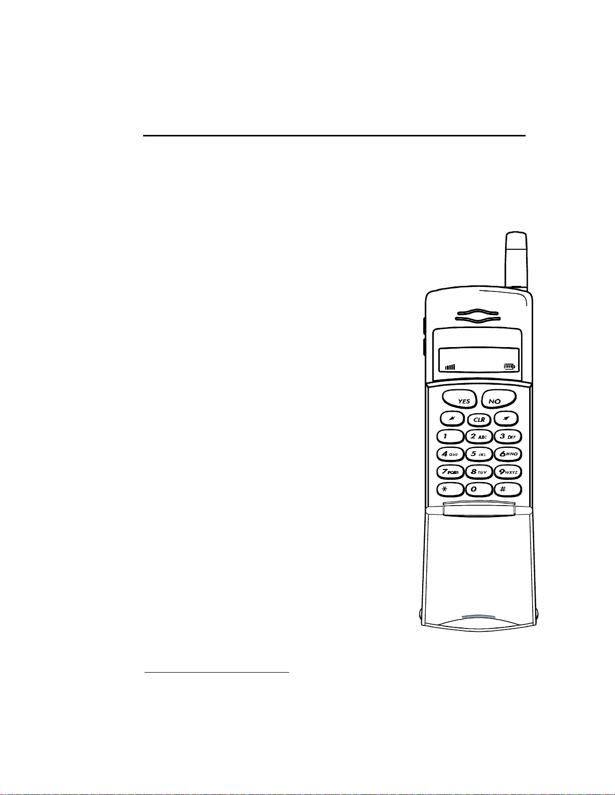
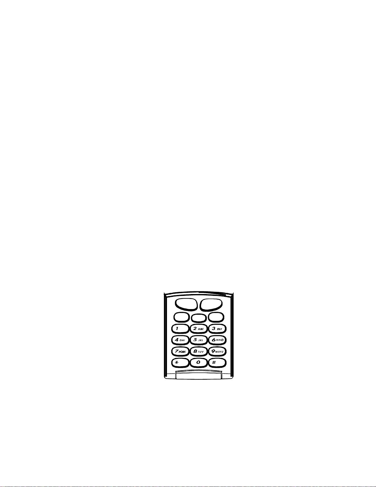
Keypad
The keypad is rubber with soft keys. See Figure 2-1. It is backlit, which makes it
possible to operate the phone in the dark. The backlight function has four possible
settings:
• On 10 seconds
• On 20 seconds
• On (when connected to external power only)
• Off
The END/PWR/NO key is not scanned, as are the other keys. It is connected to a
power switch such that microprocessor power is forced on when this key is held
down. The microprocessor can also see this key indirectly to implement the OFF
function.
SEND
END PWR
YES
NO
MEM CLR MENU
Figure 2-1. Keypad
2-3
Page 8
EN/LZB 119 2506 R1A Technical Description
READY
1
2
3
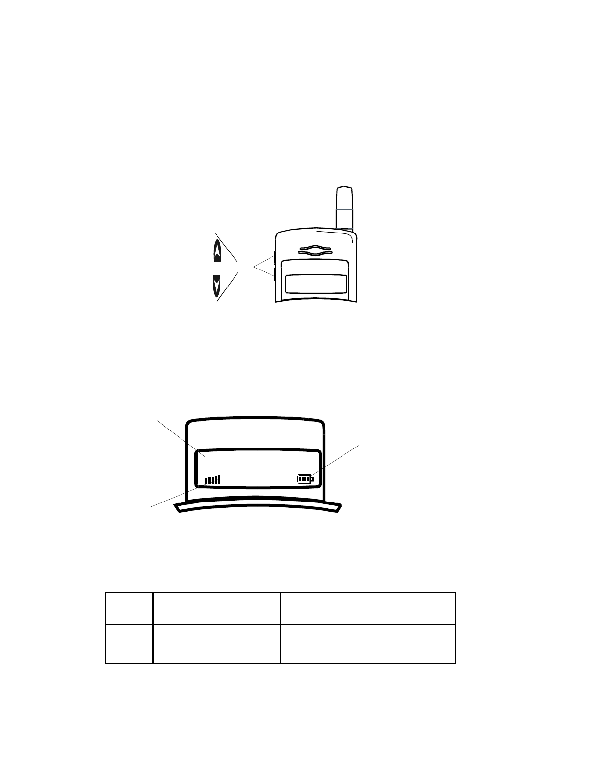
Side Volume Keys
See Figure 2-2. The volume keys are separate from the main keypad. They are push
button switches mounted on the side of the phone near the upper left corner of the
LCD.
SIDE
VOLUME
KEYS
Figure 2-2. Side Volume Keys
LCD
The phone has a 1-line LCD containing icons as well as numbers and alpha
characters. See Figure 2-3 and Table 2-2.
Figure 2-3. LCD Display
Table 2-2. LCD Display Areas
Fig.
Ref. Description Function
1 Number/Character Display Displays number or character entered
2 Battery Strength Icon Displays relative strength of battery
3 Signal Strength Indicator Displays signal strength (up to 5 bars)
2-4
Page 9
Technical Description EN/LZB 119 2506 R1A
Top Indicator
A multi-color light emitting diode (LED) is located on the top front of the phone.
Refer to Table 2-3.
Table 2-3. Top Indicator Functions
Light Indicates
Green - slow blink Ready. Phone is ready to make/receive calls.
Green - fast blink There is an incoming call or you have answered an
incoming call.
Green - steady Battery is charging and phone is ON.
Red - blinking Battery power is low.
Orange – Slow blink* Alert Option (Menu 16) is set to vibrate only.
Orange – Fast blink*
Orange – Steady* Alert option – vibrator only. Battery charging.
No light
* AF778 Only
Alert option (Menu 16) is set to vibrate only, and there is
an incoming call, or you have answered and incoming
call.
Phone is OFF, no signal is available, or phone is in
CHARGING ONLY mode.
2-5
Page 10

EN/LZB 119 2506 R1A Technical Description
Vibrator Motor (AF778 Only)
The AF778 cellular phone has a vibrating motor as an option for silent ring
indication. When the vibrating motor is activated (Menu 16), the unit will vibrate
three times when receiving an incoming call. It will also vibrate when the phone is
first turned on.
Retractable Antenna
Both the AF738 and the AF778 feature a retractable antenna. The AF738 is 1/4 wave
in both the up (extended) and the down (retracted) positions. The AF778 is 1/4 wave
in the down position and 1/2 wave in the up position.
The AF778 uses a new design consisting of a molded antenna base with a metallic
contact ferrule, and a retractable whip consisting of a helical coil, an overmolded
whip cap, and an exposed metallic upper contact ring.
This design allows the antenna to operate in 1/4 wave and 1/2-wave modes while
requiring a single RF feed.
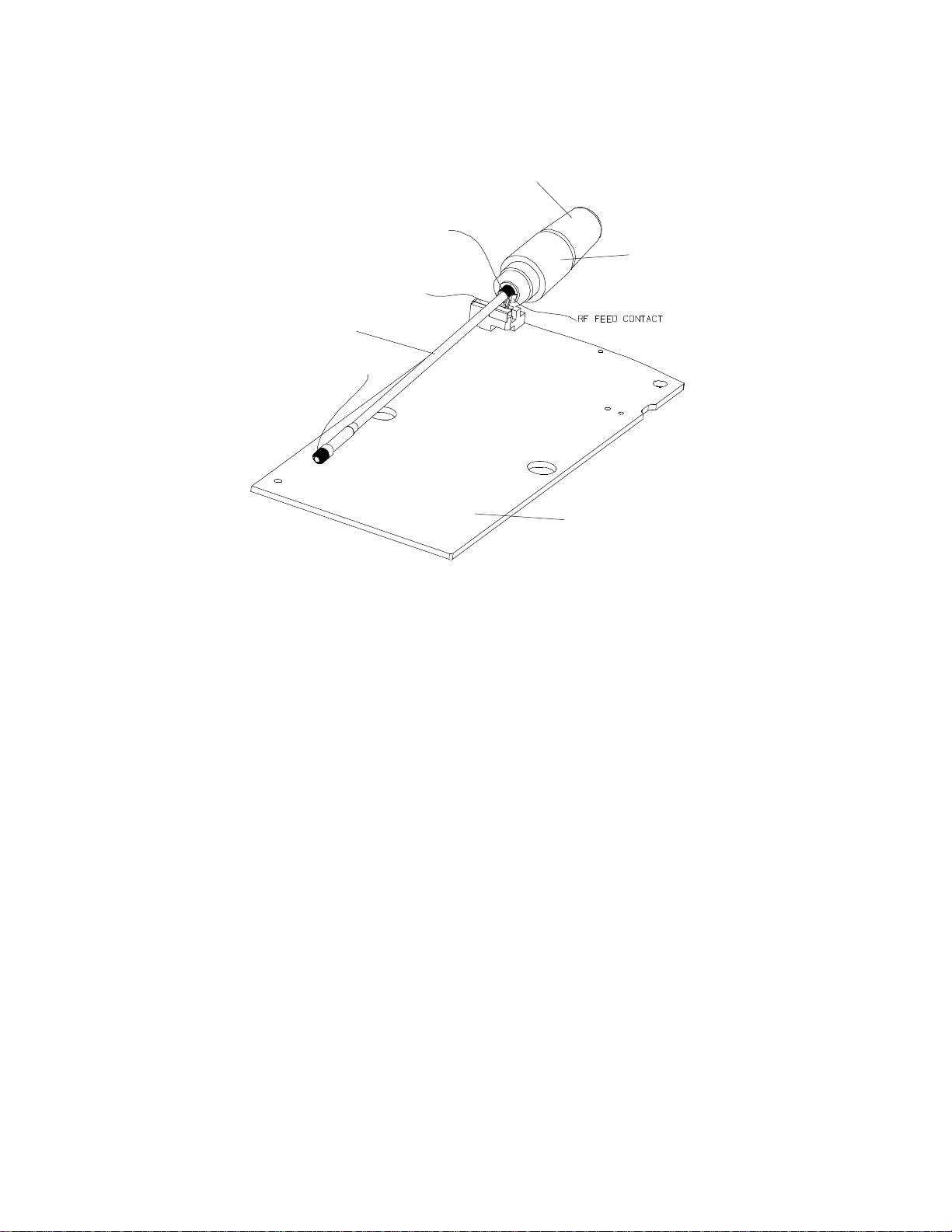
1/4 Wave Antenna Operation
In the retracted position, the AF778 operates in 1/4 wave mode. The helical coil
contacts directly to the ferrule on the antenna base. The contact ferrule makes a direct
connection to the RF feed on the antenna connector. This in turn provides a path to
the RF feed point on the PCB. The end of the whip is grounded to the PCB via a
grounding clip. See Figure 2-4.
2-6
Page 11
Technical Description EN/LZB 119 2506 R1A
PCB
HELICAL COIL
ANTENNA BASE
CONTACT FERRULE
GROUND CONTACT
(NOT CONNECTED WHEN RETRACTED)
ANTENNA MAST
BOTTOM CRIMP CONTACT
(ANTENNA GROUND)
Figure 2-4. AF778 1/4 Wave Antenna Connections
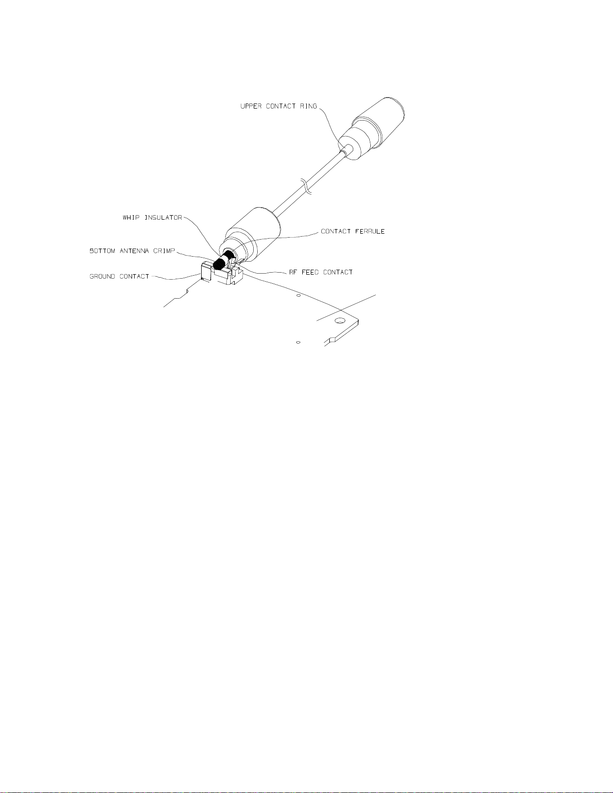
1/2 Wave Antenna Operation (AF778)
The helical connection to the PCB is broken when the antenna is extended. The
contact ferrule, however, remains in contact with the RF feed contact on the PCB.
The connection from the RF contact on the PCB and the antenna is made (via a
capacitive coupling) through a dielectric insulating material to the antenna rod. Since
the antenna mast is connected to the top helical coil, the antenna becomes an
effective 1/2-wave antenna.
The bottom crimp contact on the antenna mast mates with shunt inductor-to-ground
contact when the antenna is extended. To prevent the bottom crimp from shorting to
the RF feed, the overmolded stepped insulator provides insulation between the two
points. The coaxial connection to the NiTi rod and the shunt inductor make up the
matching network. See Figure 2-5.
2-7
Page 12
EN/LZB 119 2506 R1A Technical Description
PCB
Figure 2-5. 1/2 Wave Antenna Connections
2-8
Page 13

Technical Description EN/LZB 119 2506 R1A
Transceiver PCB and Component Layout
The transceiver consists of one PCB for both the RF and logic sections. The board is
a six layer PCB. Layers two and five act as ground planes, while layer three serves
as a plane for signal conductors.
The basic circuits of the phone are:
• RF Section
Receives and generates the RF signals needed to establish a duplex link
between the cellular mobile and base station
• Logic Section:
Digital Logic
Controls and supervises transmission/reception on the radio channel. It
also handles keyboard, display, and protocol transmission to the base
station.
Analog Logic (Audio)
Handles audio signals for earpiece, microphone, and the modem.
See Figure 2-6. Most of the components are located on the primary side of the PCB.
A few surface mount devices (SMDs) are located on the secondary side, such as the
buzzer and Power Amplifier (PA). Pads for the keyboard are also on the secondary
side.
2-9
Page 14

EN/LZB 119 2506 R1A Technical Description
Secondary Side
SYSTEM
CONNECTOR
CONNECTOR
MICROPHONE
VIBRATOR CONNECTOR
LCD
CONTACTS
DISPLAY
BACKLIGHT
KEYPAD
KEYPAD
HALL-EFFECT
Major Components
The circuitry is based mainly on CMOS components. This minimizes current
consumption so the battery may last longer. The components are in SMD packages,
which are more cost/size effective than components mounted through the board.
To minimize the size of the board and number of components, Application Specific
Integrated Circuits (ASICs) have been designed and used. These, along with other
major components, are shown in Figure 2-6 and listed in Table 2-4.
SHIELD CAN
OUTLINE
X301
Z211
Z231
BATTERY
CONTACTS
ANTENNA STRAW
GROUND STRAP
X704
(AF778 ONLY)
Z300
N211
G401
Z204
N401
Z206
N201
N702
N402
N703
N705
D603
D601
N500
D602
VOLUME
SWITCHES
B401
N701
CONTACTS
(17)
(AF778 ONLY)
X703
SPEAKER
B502
H802
BUZZER
N301
SWITCH
FOR FLIP
Primary Side
X701
(10)
LEDS
LEDS
Figure 2-6. PCB Component Layout
2-10
Page 15

Technical Description EN/LZB 119 2506 R1A
Table 2-4. Component Table
Section Reference Name Function
Radio B401 Crystal Reference oscillator, 14.85 MHz,
heart of discrete VCTCXO circuit
G401 VCO Main Voltage Control Oscillator
N201 IF IC RX Back end
N211 Annika RX Front end
N301 PA Power Amplifier (GaAs FET IC)
N401 Malin TX mixer, TX VCO, TX/RX
buffers
N402 Bertindy Radio interface to Logic,
synthesizers
N702,
Voltage Regulators
N703, N705
Z204 450 KHz Filter
Z206 2nd IF Filter
Z211 Filter RX
Z231 45 MHz
1st IF Filter
Filter
Z300 Duplexer TX/RX Filter
Logic/
Baseband
D601 Flash
EPROM
Memory - system program
D602 EEPROM Memory - Customer data
D603 Gustav Master logic control (includes
microprocessor)
N500 Anton Audio control
N701 Mia Charging functions
Connectors B502 Speaker
Makes contact with speaker
Connector
H802 Buzzer Emits ringer, alert tones
X301 Antenna
Makes contact with antenna
Connector
X701 System
Connector
Connects PCB to user interfaces,
outside peripherals, charging
functions.
X703 Vibrator
AF778 only
Connector
X704 Antenna
AF778 only
Straw
Groundstrap
2-11
Page 16

EN/LZB 119 2506 R1A Technical Description
2-12
Page 17

Technical Description EN/LZB 119 2506 R1A
Figure 2-7. Block Diagram
2-13
Page 18

EN/LZB 119 2506 R1A Technical Description
2-14
Page 19

Technical Description EN/LZB 119 2506 R1A
Radio Section
General
See Figure 2-5. This section includes information about the following:
• Duplexer
• Receiver
Receive front end
IF section
• Synthesizer
• Transmitter
Refer to Table 2-5. The radio section of the phone contains all circuitry necessary for
receiving and transmitting the RF signal. The radio operates in the AMPS frequency
bands. These frequencies make up 832 duplex channels.
Table 2-5. Frequencies
Type Measurement
Transmit frequencies 824.04 to 848.97 MHz
Receive frequencies 869.04 to 893.97 MHz
Duplex separation 45 MHz
Channel spacing 30 KHz
2-15
Page 20

EN/LZB 119 2506 R1A Technical Description
Duplexer
See Figure 2-7. The duplex filter consists of a three-pole TX filter section and a fourpole RX filter section.
The TX filter section suppresses wide band noise evolving from the VCO and the
power amplifier on RX frequencies.
The RX filter section suppresses the transmitter signal. This suppression must be at a
level low enough not to overdrive the receiver front-end amplifier.
The duplexer's out-of-band impedance is an integral part of the PA design. The
circuit is designed to protect the PA from ever seeing potentially damaging
impedances.
A high-pass element of the duplexer TX branch also provides protection against
Electro Static Discharge (ESD).
Receiver
The main components in the receiver include:
Receive front end
• ANNIKA IC
- Low Noise Amplifier (LNA)
- Mixer
• Bandpass filter
IF section
• Bandpass filter - 45 MHz
• IF IC
- 2nd Mixer
- IF AMP
- RSSI circuit
• Bandpass filters (two) - 450 KHz
2-16
Page 21

Technical Description EN/LZB 119 2506 R1A
Receive Front End
See Figure 2-7. The receiver (RX) front end is the first link in the receiver chain. Its
amplifies the RF and down-converts it to the first IF frequency. The desired
frequencies are within the range of 869 to 894 MHz.
The received signal from the antenna is fed to ANNIKA via the duplexer. The LNA,
in ANNIKA, is followed by an external bandpass filter (869-894 MHz). This filter is
needed for spurious response rejection (suppression of the first image frequency).
From the BP filter, the signal is then fed to the active mixer section of ANNIKA. The
1st LO (914-939 MHz) is generated from the RX VCO. Together with the RX
synthesizer, ANNIKA down converts the received signal to 45 MHz (first IF).
The signal then proceeds to the IF section.
IF Section
See Figure 2-7. The IF section is the second link in the receiver chain, performing the
major part of RF amplification and all the channel filtering.
The first IF (45 MHz) is filtered, buffered, and fed to the second mixer where it is
down converted to 450 kHz (2nd IF) in the IF IC. The second LO (44.55 MHz), for
the second mixer, is generated in BERTINDY by multiplying the 14.85 MHz
VCTCXO signal by three.
From the IF section, the 450 kHz signal is filtered, then fed to the digital
discriminator in BERTINDY for demodulation. The signal is also used in the AFC
circuitry to determine frequency error of the 14.85 MHz reference relative to the
received signal.
A received signal strength indicator voltage (RSSI) is generated by the IF IC, while
the FM detection and RSSI A/D conversion is done in the BERTINDY ASIC.
Further audio processing of the discriminator signal is performed in the ANTON
ASIC.
2-17
Page 22

EN/LZB 119 2506 R1A Technical Description
Synthesizer
The main components of the synthesizer include:
• VCTCXO
• BERTINDY
- RX (main) synthesizer (used for first LO signal)
- TX (auxiliary) synthesizer (used for 90 MHz signal)
- Reference divider
• MALIN
- TX VCO
- TX buffer stage
- TX mixer
- RX buffer stage
- RX prescaler
VCTCXO
A frequency reference signal of 14.85 MHz, common to the two synthesizers, is
generated by a Voltage Controlled Temperature Compensated Crystal Oscillator
(VCTCXO) and buffered in BERTINDY. This phone uses a discrete VCTCXO
circuit with a 14.85 MHz crystal at its heart.
The task of the TCXO is to supply the synthesizer with a stable, accurate reference
frequency. The TCXO frequency stability is controlled by DACs in BERTINDY. A
software algorithm is used for temperature compensation as well as an automatic
frequency control (AFC) function.
2-18
Page 23

Technical Description EN/LZB 119 2506 R1A
BERTINDY
BERTINDY is a new ASIC which combines the functions that both the BERTRAM
and CINDY ASICs performed in previous generation phones.
BERTINDY performs the following functions:
• Control logic inputs and outputs from the microprocessor
• Output power detection and control
• Received signal strength (RSSI) A/D conversion
• 450 kHz signal prescaling (for AFC and data modem) to 54 kHz
• Discrimination of the 450 kHz frequency and filtering of the audio signal
• Buffering of the 14.85 MHz reference signal (VCTCXO) to synthesizers
• Control signals (D/A converted) to VCTCXO for frequency set
• Battery voltage A/D conversion
• A/D conversion of levels for handsfree audio
• Control of VTX/V
• Digital output to control power sources, synthesizer turn on/off, power
amplifier turn on/off
Serial data communication is used for the interface between BERTINDY and the
logic section.
RX
RX (Main) Synthesizer
The task of the RX (main) synthesizer is to supply the RX and TX mixers with local
oscillator (LO) signals. The RX signal is 45 MHz above the chosen receiver
frequency (1st RX IF). The TX signal is 90 MHz above the chosen TX frequency
(TX IF). The desired frequency is set from the logic section.
The synthesizer's reference signal comes from the 14.85 MHz VCTCXO. The main
synthesizer has a speed-up mode, which allows it to get a fast lock-in time at
synthesizer start-up. This provides current savings by shutting down during repeated
overhead messages.
The main synthesizer is locked if the radio can tune to a control channel and correctly
decode the data being sent and correctly decode the SAT. On the TX synthesizer, the
control voltage for the TX VCO is continuously monitored by the microprocessor to
check that it is within an allowable range. If the control voltage outside the range, the
TX is turned off.
2-19
Page 24

EN/LZB 119 2506 R1A Technical Description
TX (Auxiliary) Synthesizer
The task of the TX synthesizer is to supply the PA stage with the TX signal at the
chosen transmitter frequency (824.04 - 848.97 MHz) in steps of 30 kHz. The
reference for the TX synthesizer comes from the 14.85 MHz VCTCXO. The TX
synthesizer creates a fixed 90 MHz signal by phase-locking a down-divided VCO
signal to the 150 kHz reference signal. The local oscillator signal is then mixed with
the 90 MHz signal to create the TX frequency signal. The TX synthesizer is
programmed from the logic section.
MALIN
The MALIN ASIC contains the TX VCO, TX buffer stage, TX mixer, RX buffer
stage, and RX prescaler. The TX VCO oscillates at a frequency determined by the
voltage at the control input. The frequency can be controlled around 90 MHz. One
part of the VCO output is fed back to the auxiliary (TX) synthesizer input of
BERTINDY. The main part of the signal is fed to the TX mixer through a low pass
filter. The signal is then mixed down with the 90 MHz TX signal to form the
transmitter frequency. Then it is passed through a bandpass filter and fed to the
discrete driver stage in the transmitter block.
Transmitter
The main component of the transmitter is the Power Amplifier (PA).
The transmitted signal is generated by the transmit synthesizer (90 MHz) and can be
modulated by an audio signal. The transmit IF (90 MHz) is mixed with the RX_LO
frequency to produce the correct transmit frequency. The signal is then fed into the
power amplifier. The output power is controlled to the appropriate level by means of
a feed back loop consisting of an op amp and a reference voltage from BERTINDY.
From the PA, the signal is fed through the duplexer to the antenna.
Power Amplifier
The PA is a GaAs FET IC with high gain and efficiency. Controlling the input drive
level varies the gain and output power. The saturated output power of the PA is
dependent upon the load presented at its output. The PA will withstand severe
mismatch (up to 7:1) at the PA output. The loss through the match, filter, and
duplexer provides sufficient return loss to ensure less than 7:1. The PA is biased
with negative voltage generated by the internal negative voltage supply.
NOTE
The PA is extremely sensitive to ESD and should not be
repaired, replaced, or probed without proper ESD-protected
equipment.
2-20
Page 25

Technical Description EN/LZB 119 2506 R1A
Logic Section
The main sections of the logic include:
• Processor/control interface
• Memories
• User interface
• Audio section
• Regulators
• Charging circuit
Processor/Control Interface
The main components of the processor/control interface include:
• GUSTAV
• 6303 Microprocessor
• ROM
• RAM
• Bus interface
• Decoder
• Serial interface
• External ports
• Watchdog
• BAR Generator
• Clock Generator
• Internal ports
• Modem
• Baudclock
2-21
Page 26

EN/LZB 119 2506 R1A Technical Description
GUSTAV
GUSTAV is an ASIC that replaces CARL (used in previous Ericsson models).
GUSTAV is the heart of the Logic section and has most digital functions "on chip".
6303 Microprocessor
• 8-bit processor
• Asynchronous full duplex serial communication interface for external
connections
ROM
• 512 byte
• Contains an interface program used for loading code into the RAM
RAM
• 6016 bytes
• Used by the processor as "working space" when the phone is turned on
• When turning off the phone, data that has to be saved is stored in the
EEPROM
Bus Interface
• Generates the data and address lines to the EPROM and internal
RAM/ROM
• Handles the internal busses in GUSTAV
Decoder
• An address decoder with address map
• Has outputs for both internal GUSTAV functions and logic control
signals
Serial Interface
• Has a transmitter block and a receiver block
• The transmitter block consists of four write registers, a clock divider, and
other logic for generating interrupts and latch signals
• The receiver block consists of three read registers in which the received
data may be read by the processor
External Ports
• Manages the keyboard along with handling binary input and output ports
2-22
Page 27

Technical Description EN/LZB 119 2506 R1A
Watchdog On/Off
• Contains the watchdog block and the autonomous time out
• The watchdog block consists of a counter that, when overflowed,
activates a reset circuit.
• The autonomous time-out (ATO) is a supervising block that monitors the
status of the received carrier detect (RXCD) and transmitter power. If TX
power is detected without the RXCD for 30 seconds, the ATO turns off
the phone.
Beep, Alarm, Ring (BAR)
• Generates a signal that can have varying tones and volumes
• The ON and OFF time can vary between 7.9 us and 2.02 ms
Clock Generator
• 8.064 MHz signal from BERTINDY is divided down and gives a system
clock frequency (E-clock) of 2.016 MHz
• Has many divider steps to generate all clock frequencies that are
necessary inside GUSTAV and other parts of the logic
Silent Ring (AF778 Only)
• A 2mA signal is sent from GUSTAV, divided down and filtered to
prevent drive circuit oscillations and ESD damage
• Signal is then sent to the vibrator motor to activate a silent ring, and to
the LED to activate the orange indicator light
Internal Ports
• Three 8-bit read and three 8-bit write ports that are used within
GUSTAV
2-23
Page 28

EN/LZB 119 2506 R1A Technical Description
Modem
Consists of:
• Data receiver
- Discriminator
- Data decoder
- Wordsync detector
• Data transmitter
• SAT detector
- SAT detection is continuous. Each measurement is 10-12 ms for the
three frequencies used (5970, 6000, and 6030 Hz).
• SAT transmitter
- SAT generation of the three frequencies
Baudclock
• Generates the baud rate (9600) for the serial interface of GUSTAV
Memories
The main components for memory include:
• RAM
• ROM
• EPROM
• EEPROM
RAM
Internal to GUSTAV.
ROM
Internal to GUSTAV.
2-24
Page 29

Technical Description EN/LZB 119 2506 R1A
EPROM (Flash)
The EPROM is a flash PROM with a 128k by 8 bit area. The phone's operating
software is stored here. Software is loaded via a serial channel into Flash EPROM.
The main purpose of software is to:
• Control the hardware circuitry
• Communicate with the cellular system via the RF link
• Provide and handle the operating interface to the user
• Overall system coordination (the phone's operating system)
• Charging of the battery
NOTE
This Flash PROM may be replaced, in time, with a one-time
programmable PROM.
EEPROM
The EEPROM is a "customer" PROM. It is a CMOS component with a 4k by 8 bit
area. Data that must be saved when the phone is turned off is stored in this memory.
The EEPROM contains the telephone number, short numbers, talk time, feature set,
and calibration information/values. The EEPROM is communicated with via a
controller in GUSTAV.
2-25
Page 30

EN/LZB 119 2506 R1A Technical Description
User Interface
The main components of the user interface include:
• LCD
• Keyboard
• Buzzer
• Vibrator Motor
• Illumination
LCD
The display is a one-row LCD. It uses chip-on-glass technology for mounting the
driver chip onto the LCD module. No negative voltage supply is required for this
LCD. Past products used a negative voltage supply to adjust the contrast of the
display because LCD technology, at the time, could not provide a viewing cone wide
enough to support all viewing angles. The LCD in this phone uses technology that
provides a much wider viewing cone, thereby eliminating the need for contrast
control.
An elastomeric connector is used for contact between the LCD module and the PCB.
Software to drive each display is contained in flash EPROM. The same version
operating software for the phone accommodates both types of LCD.
Keyboard
The basic keyboard pattern is printed on the gold plated PCB, which ensures contact.
There is also a connection for different keyboard layouts. Besides the keyboard
matrix, connections exist for illumination LEDs.
Buzzer
A buzzer in the transceiver generates the acoustic signals. The buzzer is an
electromagnetic resonance type. It has a resonance frequency of about 3 kHz. The
buzzer generates Beep, Alarm, and Ringing signals. The sounds are generated in
GUSTAV by software control and transmitted to the buzzer on the BAR signal.
The acoustic level as well as the frequency of the signal is variable. The user can turn
off all signals to the buzzer via the User Menu options. The different acoustic signals
are:
• Ringing signals
• Alarm signals
• Low battery warning
• Keypad tone or click
2-26
Page 31

Technical Description EN/LZB 119 2506 R1A
Illumination
The phone is illuminated with 14 chip LEDs: four for the display and ten for the
keyboard. The LEDs are switched on and off from GUSTAV. A voltage regulating
circuit is used to prevent changes in backlight intensity due to changes in battery
voltage.
There is also a double chip LED on the top of the transceiver. Refer to Top Indicator.
Vibrator Motor (AF778 Only)
The vibrator motor is located in the rear assembly of the phone. It is activated
through GUSTAV when the phone is set to either Vibrate/Ring or Vibrate Only, and
the phone receives a call.
Audio (Baseband) Section
The baseband audio processing circuitry is concentrated on the lower part of the
PCB. The ANTON ASIC is the heart of the audio section. The main part of the audio
frequency filtering and audio path switching is done in the ANTON ASIC.
ANTON performs the following analog functions:
• Audio filters
• Amplifiers
• Pre-emphasis and switches
• DTMF generator
• Handsfree circuitry
• Compressor/expander
Receive Audio
The discriminator output from BERTINDY is routed through a de-emphasis network
where the received SAT is separated from the speech audio. Speech audio is routed
to the speaker and SAT processing is done in GUSTAV.
The driver used for the earpiece speaker is also used to generate the Audio From
Mobile Station (AFMS) signal. This signal is routed to the system connector for use
by accessories and test equipment.
Transmit Audio
The microphone input, SAT tones, and data have separate signal paths and
adjustments. They have no limiters. Adjustment is independent and does not interfere
with audio deviation.
2-27
Page 32

EN/LZB 119 2506 R1A Technical Description
Power Supplies
Regulators
Three 50-mA regulators power the phone: VDIG, VMALIN, and VRAD. The VDIG
regulator is used to power the digital, audio, and user interface circuitry. VMALIN
powers Malin TX and buffer. VRAD powers the remaining radio circuitry. These
regulators are on all the time (even during charging-only mode) except when the
transceiver is turned off and not connected to a charger.
Reset
A low-voltage detector in ANTON monitors the digital voltage VDIG. While the
phone is operating, if VDIG drops below 3.35V (typical), ANTON will cause the
processor to reset. Upon power-up, this reset is held low for a 20 ms delay.
On/Off Control
The phone may be powered on by either pressing the END/PWR/NO key, or by
applying 7v to 10v at DCIO.
The END/PWR/NO key powers the phone by connecting the voltage at VBATT to
the regulator's enable input through a diode. The END/PWR/NO key must be held for
at least 200 ms.
Chargers and accessories power the phone by applying 7v to 10v at DCIO. As with
the END/PWR/NO key, the DCIO voltage must be present for at least 200 ms in
order to power up the phone.
If the battery is dead (less than 4.0v), applying high voltage to DCIO will not power
the phone immediately. The regulator enable is held low until the battery charges up
to 4.2v via a trickle resistor. When the battery voltage reaches 4.2v, the regulators are
enabled.
If a charger is not connected, the phone is powered off by holding, then releasing, the
END/PWR/NO key. Pressing the END/PWR/NO key generates an interrupt to
GUSTAV. The regulators will stay on until the END/PWR/NO key is released.
The phone does not turn completely off while a charger and battery are connected.
The charging circuit will be active, and CHARGING ONLY will be displayed.
See also Charging Circuit.
2-28
Page 33

Technical Description EN/LZB 119 2506 R1A
Transient/ESD Protection
Diodes are used for ESD protection on system connector outputs. Inputs have 100K
series resistance between the system connector and the ASIC input ports. Should a
high-energy surge occur when the charging FET switch is on, the battery absorbs the
energy and prevents the voltage from rising too high. Capacitors on DCIO prevent
spikes due to charger cable inductance when the charge switch is turned off. They
also protect MIA and the FET switch from ESD. Additional high-voltage and ESD
protection is provided on VBATT.
Charging Circuit
The phone software controls charging by turning a FET switch on/off, based on
battery voltage and charging current through a sense resistor. Chargers are designed
to have an open-circuit voltage less than 10v, and supply an average current of
approximately 700 mA (200 mA for slow charger) when connected to a battery. A
dead battery is allowed to trickle charge high enough for the phone to turn on.
The MIA ASIC provides charge switch control and analog outputs corresponding to
charger current and battery voltage. These outputs are connected to BERTINDY's
A/D inputs. GUSTAV turns on the charge switch using an output port connected to
MIA. If VBATT <8v, GUSTAV controls the on/off state of the FET switch. If
VBATT >8.0V, MIA keeps the charge switch off regardless of the state of
GUSTAV’s output port.
2-29
Page 34
EN/LZB 119 2506 R1A Technical Description
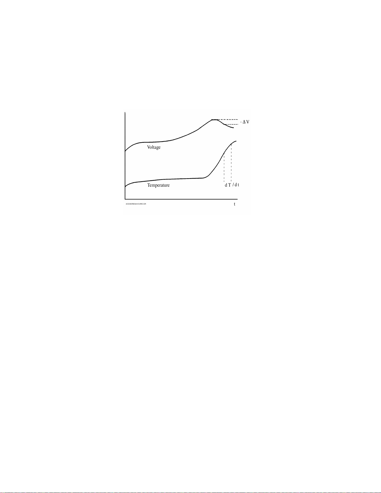
Rapid Charging
See Figure 2-8. The charging current varies from 600 to 1000mA. The processor
measures the battery voltage continuously during the charging process.
Figure 2-8. Rapid Charging
Several algorithms are used to determine when the battery is fully charged, for
example:
• Minus Delta V
• Flat V
• Maximum Voltage
• Safety Timer
The safety timer terminates the charging after four hours of charging.
Trickle Charging
When the main charging is completed, a trickle charge is started to maintain the
battery.
2-30
Page 35

Technical Description EN/LZB 119 2506 R1A
Connections On The Transceiver Board
Antenna Connector
The antenna connector consists of a mechanical assembly that connects the antenna
to the signal point on the PCB. The impedance of the antenna connector is 50 ohms.
Battery Contacts
• + Connects the (+) pole of the battery to V
• - Connects the (-) pole of the battery to GND.
BATT
Speaker Connector
The speaker connector is located at the top of the PCB. It is a four-pin connector that
interfaces the radio section of the PCB with the speaker of the phone.
LCD Contacts
Three gold LCD contacts on the PCB make contact with the LCD assembly
elastomer
Microphone Connector
The microphone is housed in the system connector assembly. It is a two-pin
connector that makes contact with the gold-plated pads on the PCB.
Vibrator Connector (AF778 Only)
The vibrator connector is located next to the speaker connector at the top of the PCB.
It is a two-pin connector, into which the vibrator wires attach.
Antenna Ground Strap (AF778 Only)
A gold contact on the antenna side of the PCB makes contact with the metalized
antenna guide straw.
2-31
Page 36

EN/LZB 119 2506 R1A Technical Description
1
Charger
12
System Connector
See Figure 2-9 and Table 2-6. The external connector (system connector) is located
on the bottom of the phone. It is a 12 pin SMT type connector with transient
protectors on all pins. Inputs are buffered to prevent accessories from feeding back
any voltages. With the system connector, the telephone communicates with external
equipment such as:
• Vehicle handsfree kit
• Portable handsfree kit
• Battery chargers
• Test equipment
Figure 2-9. System Connector
Table 2-6. System Connector Signals
Pin Signal Function In/Out
1 AFMS Audio From Mobile Station O
2 ATMS Audio To Mobile Station I
3 EXTAUD External audio sense for accessories I
4 AGND Signal Ground 0v (analog) -5 PORTHF Portable handsfree sense I
6 MUTE Signal control for external music mute O
7 --- Not Used -8 V
DD
Digital voltage O
9 DFMS Data From Mobile Station O
10 DGND Digital ground and DC return -11 DTMS Data To Mobile Station I
12 DCIO 1. Charger input
2. Output voltage to some accessories
I
O
2-32
Page 37

Technical Description EN/LZB 119 2506 R1A
Specifications
System Used AMPS
Frequency Range TX 824.04 - 848.97 MHz
RX 869.04 - 893.97 MHz
Number of Channels 832
Channel Spacing 30 kHz
Duplex Spacing 45 MHz
Modulation Method FM
Voltage 4.2 VDC - 6.0 VDC (4.8 VDC nominal)
TX Current (Illumination off)
Standby Current (Illumination off)
Vibrator Current (On)
(AF778 only)
Transmit RF Output Power (Max.)
Output Impedance 50 Ohm
Receive Sensitivity > 12 dB SINAD @ -116 dBm
400 mA ± 100 mA (PL2)
55 mA ± 10 mA (scanning)
25 mA ± 10 mA (locked on signal)
110 mA, ± 20mA
400 mW ± 80mW
26 dB ± 1 dB
2-33
 Loading...