

Page 1

Trouble Shooting Guide, Advanced
Trouble Shooting Guide, Advanced
by Toko (toko@gsm-free.org)
4/00021-3/00021/16 C Approved according to 1776-3/FEA 209 544
Page 2

Trouble Shooting Guide, Advanced
Contents
1 Explanations........................................................................................................................3
2 Enter Test Program............................................................................................................7
3 Calibration IQ...................................................................................................................12
4 TxVCO...............................................................................................................................14
5 VCXO.................................................................................................................................19
6 Calibration RSSI...............................................................................................................23
7 Power Level Calibration...................................................................................................25
8 Intermediate Power Calibration......................................................................................30
9 Transient Spectrum (Spectrum due to Switching).........................................................31
10 Modulation Spectrum Switched Mode (Spectrum due to Modulation)......................36
11 EE-prom ............................................................................................................................45
12 ADC Calibration (Voltage Calibration)..........................................................................46
13 Current Calibration..........................................................................................................49
14 Network Problems ............................................................................................................53
15 Phase and Frequency Error.............................................................................................62
16 Output Power....................................................................................................................63
17 Burst Timing (Power Time Template)............................................................................67
18 Sensitivity (Rx Quality) ....................................................................................................69
19 Rx Level.............................................................................................................................74
20 Audio..................................................................................................................................76
21 Keyboard...........................................................................................................................83
22 Display................................................................................................................................85
23 Buzzer ................................................................................................................................89
24 Illumination.......................................................................................................................90
25 Top Indicator.....................................................................................................................92
26 SIM Problems (“Insert card”).........................................................................................94
27 Selftest................................................................................................................................97
28 ADC Values.......................................................................................................................99
29 Revision History..............................................................................................................102
4/00021-3/00021/16 C 2(102)
Page 3

1 Explanations
1.1 Conditions
All measurements described in this Trouble Shooting Guide – Advanced, are performed in
EFRA with test program in the phone. Some of the faults can occur in tests without test
program, e.g. Go/No Go -tests. In these cases you have to program the phone with test program
before starting to trouble shoot using this guide.
For trouble shooting with signal program, see 4/00021-2/FEA 209 544/16.
For component placing see1078-2/FEA 209 544/16.
In case of liquid damage no further action should be taken, handle the unit according to the local
company directives.
When measuring with the probe, remember to set the correct attenuation (ext. preamp. gain) on
the spectrum analyzer. To get the most appropriate value, set the gain according to Tx output on
a correct working card.
Trouble Shooting Guide, Advanced
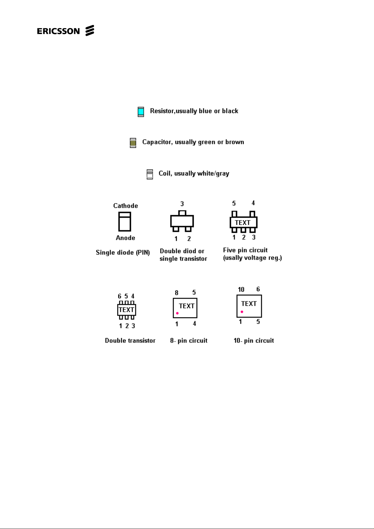
1.2 Abbreviations
B: Crystal.
C: Capacitor.
D: Digital circuit.
F: Over voltage protection.
H: Buzzer, LED and pads for display.
J: Connector.
L: Coil.
N: Analogue circuit.
P: Test point.
R: Resistor.
S: Keyboard pads.
U: BALUN Component that converts a balanced signal to an unbalanced or the other way
around.
V: Transistor or diode.
X: Contact surface on the circuit board.
Z: Filter.
4/00021-3/00021/16 C 3(102)
Page 4

Trouble Shooting Guide, Advanced
AGND: Ground for analogue signal.
AFMS: Audio from mobile station.
ATMS: Audio to mobile station.
DCIO: DC voltage through the system connector for charging.
GND: Ground.
LED3K: Logical signal that activates the background illumination.
ONSWAn: Voltage from the On/Off key that starts the phone.
RTC: Real Time Clock. The clock that keeps track of time and date.
SIMCLK: Signal from the processor used for communication to SIM, clock signal.
SIMDAT: Signal from the processor used for communication to SIM, data signal.
SIMRST: Signal from the processor used for communication to SIM, r eset signal.
SIMVCC: Feed voltage for SIM.
VBATT: Battery voltage (4.8V)
VCORE: DC voltage for the processor and memory (2.5 V)
VDIG: DC voltage for the processor and memory (3.2 V)
VLCD: DC voltage for the display that controls the contrast.
VRAD: DC voltage for the radio part except the synthesiser. (3.75 V)
VRTC: DC voltage for the real time clock. (2.5 V)
VVCO: DC voltage for the synthesiser (3.75 V)
I2C: Communications standard for two-way communication using only 2 wires,
clock and data.
4/00021-3/00021/16 C 4(102)
Page 5
1.3 Pin placing
Trouble Shooting Guide, Advanced
4/00021-3/00021/16 C 5(102)
Page 6

Trouble Shooting Guide, Advanced
4/00021-3/00021/16 C 6(102)
Page 7

2 Enter Test Program
2.1 Introduction
To be able to use EFRA, the phone has to be programmed with test program. The programming
is also performed in EFRA.
If the phone cannot be programmed, proceed to section 2.3.
If the phone does not start in the radio calibration or trouble shooting part of EFRA, despite an
approved flash programming, proceed to section 2.2.
2.2 The phone does not start in the test program
Trouble Shooting Guide, Advanced
Attach a dummy battery and press the On/Off button. Check the display and the current
consumption.
If the phone starts (showing the revision of the test program in the display) and consumes 30 –
50 mA, the phone is usually without fault.
Check your equipment.
The following things are necessary for the phone to start in the test program:
Correct battery voltage (4.8 V).
Correct feed voltage to the trouble shooting box (15 V).
The current limitation must be set high enough on both outputs of the power amplifier (2A).
The phone must be started before clicking on the ”Startup” in EFRA.
The following signal must be found at the system connector of the phone: TTMS, TFMS,
VPPFLASH, GND and VDD.
Correct serial port of the trouble shooting box chosen.
”Mode”-switch should be in position ”Service”.
A Hardlock connected and installed.
If the fault really is electrical, open the phone and make a visual check of the board.
Make sure that there is not any liquid damage, burned or damaged pads at the system connector
or bad soldering of e.g. D600 or D610.
Power up the board and start it by using a pulse at the DCIO (or the On/Off button).
Check the amplitude of MCLK at C680 using the spectrum analyser (>3 dBm). We have been
using the following settings: CF – 13MHz, SPAN – 1 MHz, RBW – 10 kHz, VBW – 10 kHz
andSWEEP–30ms.
If MCLK is too low, the fault usually is due to L340, B301 or a s hort circuit in C343.
If the fault still remains, try to program the phone again.
If the phone consumes more then 200 mA, proceed to section 2.4.3.
If the phone consumes no current at all, when the button is pressed, open the phone and check
for liquid damage. Also make sure that the keyboard and the keyboard pads are okay and that
they are clean.
4/00021-3/00021/16 C 7(102)
Page 8

If there is a signal program in the phone, you have to program it with the test program.
2.3 The phone cannot be programmed
Makesurethat:
the battery screws are okay and tightened;
the system connector is not dirty or liquid damaged.
Attach a dummy battery. If the phone consumes current immediately, the fault is usually due to
a short circuit of VBATT, but first you must make sure that the isolation of the frame is not in
contact with the plus pole of the board.
Trouble Shooting Guide, Advanced
Start the phone with the On/Off button and check the current consumption.
If the phone consumes no current at all when the button is pressed, there is probably liquid
damage. Open the phone and check for liquid damage. Also make sure that the keyboard and the
keyboard pads are okay and that they are clean.
If the phone consumes more then 200 mA, proceed to section 2.4.3.
If the phone does not start, try to program it on board level.
If the phone does not start in the flash programmer, proceed to section 2.4.1.
If the phone can be programmed, but does not start afterwards or is troublesome in the flash
programmer, proceed to section 2.4.2.
If the phone starts after programming, the fault is probably solved, but to eliminate the
possibility of intermittent faults make sure that the soldering at D600, D610 or D630 are correct.
4/00021-3/00021/16 C 8(102)
Page 9

2.4 Measuring at a powered circuit board
2.4.1 Does not start in the flash programmer
Make sure that the pads of the system connector are not burned or in any way damaged.
Attach the board to the fixture. Power up the board by keeping DCIO high.
Measure the voltages VDIG (3.2 V) and VCORE (2.5 V).
If any of the voltages are too low, measure the resistance to ground (VDIG > 1 kohm, VCORE
> 25 kohms).
If the resistance is correct, replace the corresponding circuit (VDIG - N701, VCORE - N700).
If the resistance is too low, use the schematics. Remove the components one by one (or lift the
pin/pins feeding the circuit), that is fed from the short circuited voltage, and measure the
resistance after each removal. You have found the faulty component when the resistance is
increasing after removal. Do not forget to mount all the components that have been removed.
You should also replace the circuits on which you have lifted the pins. The short circuit is
usually due to D610, D600 or any of C600, C602-C611, C614, C800, C802-C807, C902, C906
for VDIG and D900 or any of C900, C901, C903-C905 for VCORE.
Trouble Shooting Guide, Advanced
If any of the voltages are too high, replace the corresponding circuit.
Measure the power reset at C710 (>3 V). If it is lower, the fault is probably due to C710 or
N550.
Measure the voltage VRAD/VVCO (3.8 V).
If the voltage is incorrect, measure the resistance between ground and N580:5 (50 kohms).
If the resistance is correct, replace N580.
If the resistance is too low, use the schematics. Remove the components one by one (or lift the
pin/pins feeding the circuit), that is fed from the short-circuited voltage, and measure the
resistance after each removal. You have found the faulty component when the resistance is
raising after removal. Do not forget to mount all the components that have been removed. You
should also replace the circuits on which you have lifted the pins. The short circuit is usually
due to N550, or any of the 10nF-capacitors on VRAD/ VVCO.
Check the amplitude of the clock, using the oscilloscope, at B301:3 (>0.7 V t- t). You can also
use the spectrum analyser to check the amplitude (>1 dBm). We have been using the following
settings for the oscilloscope: CF – 13MHz, SPAN – 1 MHz, RBW – 10 kHz, VBW – 10 kHz
and SWEEP – 30 ms. A fault of the clock can be due to L340, B301 or a short circuit in C343,
D600, N300 or C300. Sometimes the fault is due to N202.
4/00021-3/00021/16 C 9(102)
Page 10

Trouble Shooting Guide, Advanced
Make sure that the soldering at D600, D610 or D630 are correct. If they are correct and all the
feed voltages and the clock are correct, the fault is usually due to D600. The fault can also be
due to D610 or D630.
Try to program the phone between each replacement.
2.4.2 Can be programmed, but does not start afterwards or is
troublesome in the flash programmer
Make sure that the pads of the system connector are not burned or in any way damaged.
Open the phone and check for liquid damage.
Attach the board to the fixture. Power up the board by keeping DCIO high.
Measure the voltages VDIG (3.2 V) and VCORE (2.5 V).
If any of the voltages are too low, measure the resistance to ground (VDIG > 1 kohm, VCORE
> 25 kohms).
If the resistance is correct, replace the corresponding circuit (VDIG - N701, VCORE - N700).
If the resistance is too low, use the schematics. Remove the components one by one (or lift the
pin/pins feeding the circuit), that is fed from the short circuited voltage, and measure the
resistance after each removal. You have found the faulty component when the resistance is
raising after removal. Do not forget to mount all the components that have been removed. You
should also replace the circuits on which you have lifted the pins. The short circuit is usually
due to D610, D600 or any of C600, C602-C611, C614, C800, C802-C807, C902, C906 for
VDIG and D900 or any of C900, C901, C903-C905 for VCORE.
If any of the voltages are too high, replace the corresponding circuit.
Measure the voltage VRAD/VVCO (3.8 V).
If the voltage is incorrect, measure the resistance between ground and N580:5 (50 kohms).
If the resistance is correct, replace N580.
If the resistance is too low, use the schematics. Remove the components one by one (or lift the
pin/pins feeding the circuit), that is fed from the short circuited voltage, and measure the
resistance after each removal. You have found the faulty component when the resistance is
raising after removal. Do not forget to mount all the components that have been removed. You
should also replace the circuits on which you have lifted the pins. The short circuit is usually
due to N550, or any of the 10nF-capacitors on VRAD/ VVCO.
Check the amplitude of the clock, using the oscilloscope, at B301:3 (>0.7 V t- t). You can also
use the spectrum analyser to check the amplitude (>1 dBm). We have been using the following
settings for the oscilloscope: CF – 13MHz, SPAN – 1 MHz, RBW – 10 kHz, VBW – 10 kHz
and SWEEP – 30 ms. A fault of the clock can be due to L340, B301 or a short circuit in C343,
D600, N300 or C300. Sometimes the fault is due to N202.
4/00021-3/00021/16 C 10(102)
Page 11

Make sure that the soldering at D600, D610 or D630 are correct. If they are correct and all the
feed voltages and the clock are correct, the fault is usually due to D600. The fault can also be
due to D610 or D630.
Try to program the phone between each replacement.
2.4.3 Consumes more then 200 mA
Open the phone and check for liquid damage.
Make sure that the pads of the system connector are not burned.
Attach the board to the fixture. Power up the board by keeping DCIO high.
Measure the voltages VDIG (3.2 V) and VCORE (2.5 V).
Trouble Shooting Guide, Advanced
If any of the voltages are too low, measure the resistance to ground (VDIG >1 kohm, VCORE
>25 kohms).
If the resistance is correct, replace the corresponding circuit (VDIG - N701, VCORE - N700).
If the resistance is too low, use the schematics. Remove the components one by one (or lift the
pin/pins feeding the circuit), that is fed from the short circuited voltage, and measure the
resistance after each removal. You have found the faulty component when the resistance is
raising after removal. Do not forget to mount all the components that have been removed. You
should also replace the circuits on which you have lifted the pins. The short circuit is usually
due to D610, D600 or any of C600, C602-C611, C614, C800, C802-C807, C902, C906 for
VDIG and D900 or any of C900, C901, C903-C905 for VCORE.
If any of the voltages are too high, replace the corresponding circuit.
Measure the voltage VRAD/VVCO (3.8 V).
If the voltage is incorrect, measure the resistance between ground and N580:5 (50 kohms).
If the resistance is correct, replace N580.
If the resistance is too low, use the schematics. Remove the components one by one (or lift the
pin/pins feeding the circuit), that is fed from the short circuited voltage, and measure the
resistance after each removal. You have found the faulty component when the resistance is
raising after removal. Do not forget to mount all the components that have been removed. You
should also replace the circuits on which you have lifted the pins. The short circuit is usually
due to N550, or any of the 10nF-capacitors on VRAD/ VVCO.
Check the amplitude of the clock, using the oscilloscope, at B301:3 (>0.7 V t- t). You can also
use the spectrum analyser to check the amplitude (>1 dBm). We have been using the following
settings for the oscilloscope: CF – 13MHz, SPAN – 1 MHz, RBW – 10 kHz, VBW – 10 kHz
and SWEEP – 30 ms. A fault of the clock can be due to L340, B301 or a short circuit in C343,
D600, N300 or C300. Sometimes the fault is due to N202.
Make sure that the soldering at D600, D610 or D630 are correct. If they are correct and all the
feed voltages and the clock are correct, the fault is usually due to D600. The fault can also be
due to D610 or D630.
Try to program the phone between each replacement.
4/00021-3/00021/16 C 11(102)
Page 12
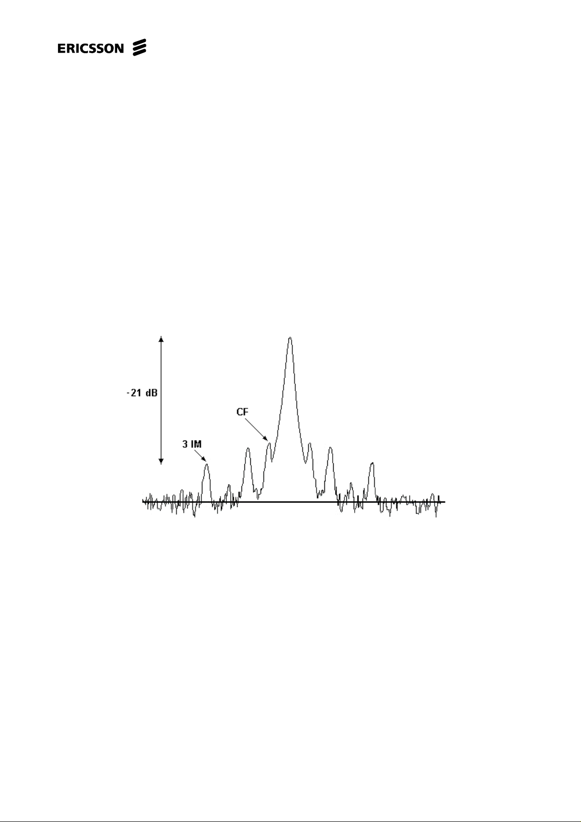
3 Calibration IQ
3.1 What is calibration IQ
The IQ-filter consists of two parts. The first part is a passive lowpass-filter between the
waveform generator in D600 and N202 consisting of R642-R645, C106 and C108. The second
part is a software- controlled filter in N202 that is calibrated with a certain test signal from the
waveform generator.
When calibrating, the transmitter is powered up in static mode with the test modulation. The
peak, that exists at CF-201 kHz related to the highest peak (CF+67 kHz), is measured, and the
LPBW/LPQ parameters in Homeros are tuned, until correct suppression (typ -21 dBm) is
obtained.
Trouble Shooting Guide, Advanced
Fig. 3.1
3.2 How to find the fault
Open the phone and check for liquid damage.
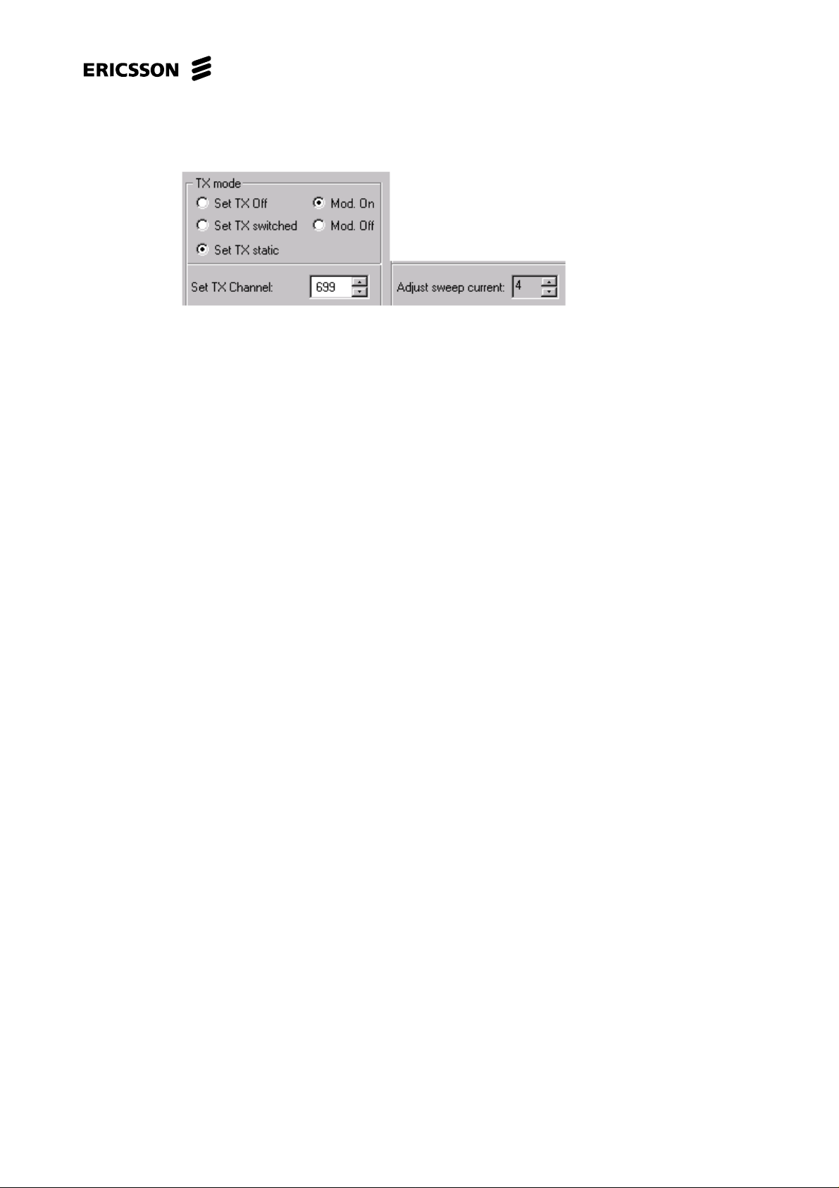
Attach the board in the fixture and start the test program.
NOTE! If the card i s of type 2, with the EKA power module, remember to attach the
negative bias voltage in the fixture.
Change the settings on the spectrum analyser to: SPAN: 1 MHz, RBW: 10 kHz, VBW:10 kHz,
SWEEP: 30 ms.
Start the transmitter in static mode with modulation on the middle channel (699) on the DCS
1800-band (Fig. 3.2). If the transmitter does not lock, decrease the sweep current.
4/00021-3/00021/16 C 12(102)
Page 13
Trouble Shooting Guide, Advanced
Fig. 3.2
Make sure that the spectrum looks like in Fig. 3.1.
If the spectrum does not look like the figure it is either one of the modulation signals (MODQN,
MODQP, MODIN, MODIP) that is missing from D600 or the lowpass-filter to the modulation
signals that is faulty (R642-R645, C106, C108).
Measure on the capacitors with an oscilloscope. The signals are sinus shaped with the frequency
67.7 kHz and the amplitude 3.0 V. Compare the signals with each other. The fault is probably
on the one modulation signal that differ from the others. If the modulation signals looks good
and are in the right phase (90 degrades turned compared to each other) then the fault could be
caused by N202.
4/00021-3/00021/16 C 13(102)
Page 14
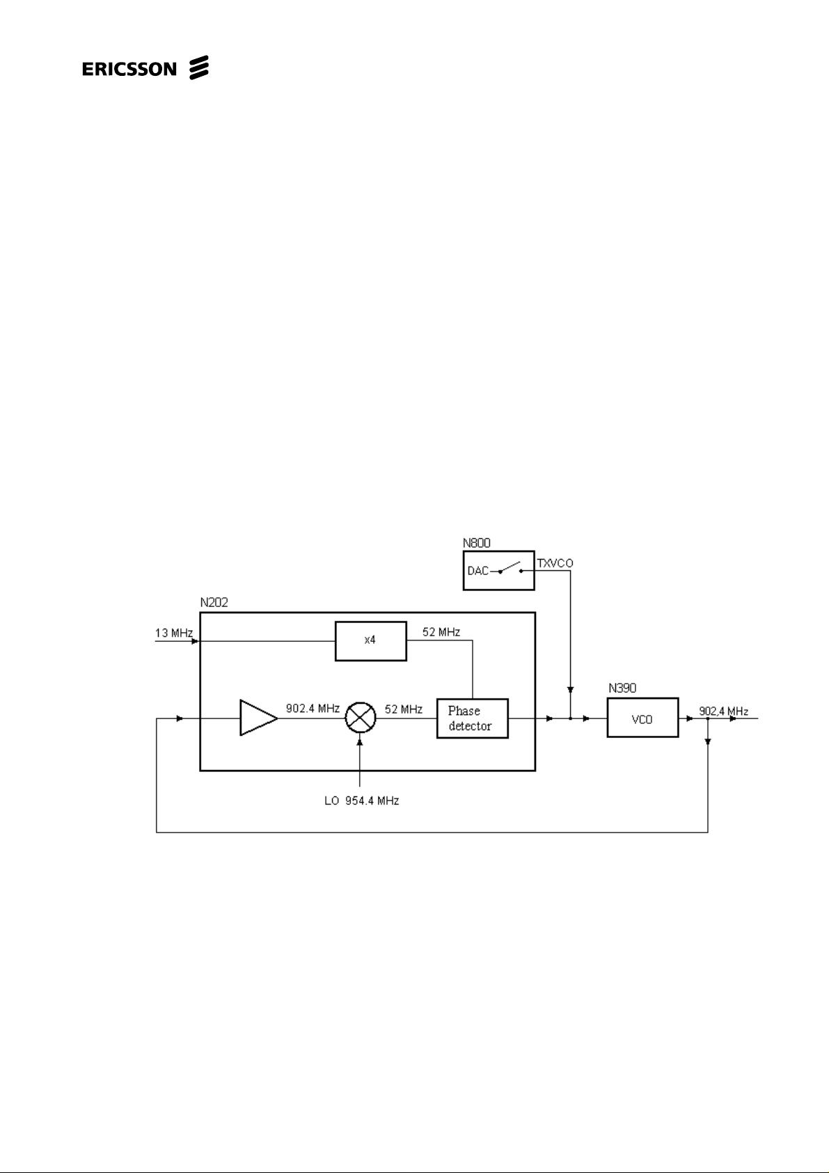
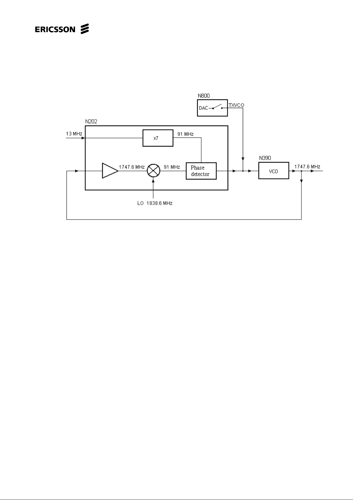
4TxVCO
4.1 What is TxVCO – Calibration
In the GSM900-system a phone can communicate with the base station at 124 frequencies in
each direction (890.2 - 914.8 MHz for the transmitter and 935.2 - 959.8 MHz for the receiver).
In the GSM1800-system it is possible to communicate at 374 frequencies in each direction
(1710.2 – 1784.8 MHz for the transmitter and 1805.2 – 1879.8 MHz for the receiver).
The communication between the base station and the phone are done switched. The system
makes it possible to change frequency between each burst. For every new burst the transmitter
synth of the phone has to lock again at the frequency the base station expects, before activating
the transmitter.
Fig 4.1 and Fig 4.2 shows two simplified diagrams over the lock-on of the Tx-synth. The
frequencies are for channel 62 (GSM900) and channel 699(GSM1800).
Trouble Shooting Guide, Advanced
GSM 900
Fig. 4.1
4/00021-3/00021/16 C 14(102)
Page 15
GSM 1800
Trouble Shooting Guide, Advanced
Fig. 4.2
The frequency of the transmitter has to lock during a predestinated time. To make the locking
time fast enough, the phone uses pre-learned TxVCO-values read from the EEPROM. The l ockon begins with the TxVCO-AC transforming a, for this particular channel, saved EEPROMvalue to a start value for the control voltage of the VCO (N390). The voltage is a little bit higher
than the expected value when the synth has locked on. By using the start value of the control
voltage the VCO generates a transmitter frequency that is only a little too high. The transmitter
frequency is fed back through a mixer to the Phase detector (both inside N202). The Phase
detector compares the mixed frequency (91 or 52 MHz) with an intern reference signal (7x13
=91 or 4x13 =52 MHz). The result of the phase comparison is a DC voltage that controls the
VCO. The TxVCO-DAC is disconnected and the Phase detector takes over the adjustment of the
control voltage to the VCO. When the transmitter synth has locked on (the Phase detector in
N202 has stabilized the control voltage and the frequency), the phone can begin to transmit.
The start value of the synth, the TxVCO value, has to be calibrated due to the differences of
tolerance in the components of the transmitter synth. The calibration i s performed in switched
mode, at two channels: for GSM900 high (channel 94 or 908,8 MHz) and low (channel 30 or
896 MHz) and for GSM1800 high (channel 826 or 1773.0 MHz) and low (channel 570 or
1721.8 MHz). The values for other channels you get by interpolation.
The tables below (Table 4.1 and 4.2) show the limits for the T xV CO – values.
4/00021-3/00021/16 C 15(102)
Page 16

GSM 900
TxVCO Min Max
Ch 30 56 A6 Hex
86 166 Dec
CH 94 6A BA Hex
106 186 Dec
Table 4.1
GSM 1800
TxVCO Min Max
Ch 570 37 87 Hex
55 135 Dec
CH 826 7E CE Hex
126 206 Dec
Table 4.2
Trouble Shooting Guide, Advanced
4.2 How to find the fault
Open the phone and check for liquid damage.
Power up the board and start the phone in the test program.
Measure the voltage at C853 and C854. Replace the corresponding capacitor if the voltage is
lower than approximately 1.1 V.
NOTE! If the card is of type 2 (roa 117 3258/2 or roa 117 3920/2), remember to attach the
negative bias voltage before changing to static mode.
GSM900:
Start the transmitter in static mode at channel 62 (902.4 MHz) and check the amplitude and the
frequency. If the frequency i s faulty, try to decrease the ”Adjust sweep current” until the
frequency of the transmitter has locked on. We have been using the following settings on the
spectrum analyser while measuring: CF- 902.4 MHz, SPAN- 200 MHz, RBW- 10 kHz, V BW10 kHz and Sweep- 30 ms.
If the transmitter locks, start the transmitter in switch mode at middle channel (62) with ”DAC 4
value” at FF. We have been using the following settings on the spectrum analyser while
measuring: CF- 902.4 MHz, SPAN- 0 MHz, RBW- 300 kHz, VBW- 100 kHz and Sweep- 0.8
ms.
Check if there is an output power (32 dBm) at the antenna plate using the spectrum analyser.
If the output power is correct, the phone is probably without fault. Try the phone in the test
again.
If there is no switched output power at all or if it i s too low, proceed to chapter 14 (”Network
problem”) section 14.3.1.
If the transmitter does not lock, start the transmitter in static mode again and change the settings
for the spectrum analyser to: 954.4 MHz, SPAN- 200 MHz, RBW- 10 kHz, VBW- 10 kHz and
Sweep- 30ms.
Check the frequency and the amplitude of the LO-signal at N331:1 (0dBm).
4/00021-3/00021/16 C 16(102)
Page 17

Trouble Shooting Guide, Advanced
If the amplitude and the frequency is correct, proceed to section 14.2.1.
If the frequency is correct, but the amplitude is too low, check the feed voltage at N331:7 (3.7
V).
If the voltage is correct, replace N331.
If the voltage is incorrect, check VVCO (3.8 V), SYNTON (3.8 V), BANDSEL and V337 with
the belonging components.
If the amplitude is correct, but the frequency is incorrect, the fault is usually due to N300. It can
also be due to N331 or D600.
If the signal is several MHz wide, replace C313.
(To make a more accurate frequency measuring, try to decrease SPAN to 1 MHz.)
GSM1800:
Start the transmitter in static mode at channel 699 (1747.4 MHz) and check the amplitude and
the frequency. If the frequency is faulty, try to decrease the ”Adj ust sweep current” until the
frequency of the transmitter has locked on. We have been using the following settings on the
spectrum analyser while measuring: CF- 1747.4 MHz, SPAN- 200 MHz, RBW- 10 kHz, V BW10 kHz and Sweep- 30 ms.
If the transmitter locks, start the transmitter in switch mode at middle channel (699) with ”DAC
4 value” at FF. We have been using the following settings on the spectrum analyser while
measuring: CF- 1747.4 MHz, SPAN- 0 MHz, RBW- 300 kHz, VBW- 100 kHz and Sweep- 0.8
ms.
Check if there is an output power (28-32 dBm) at the antenna plate using the spectrum analyser.
If the output power is correct, the phone is probably without fault. Try the phone in the test
again.
If there is no switched output power at all or if it i s too low, proceed to chapter 14 (”Network
problem”) section 14.3.1.
If the transmitter does not lock on, start the transmitter in static mode again and change the
settings for the spectrum analyser to: 1838.6 MHz, SPAN- 200 MHz, RBW- 10 kHz, VBW- 10
kHz and Sweep- 30ms.
Check the frequency and the amplitude of the LO-signal at N330:1 (0dBm).
If the amplitude and the frequency are correct, proceed to section 14.2.2.
If the frequency is correct, but the amplitude is too low, check the feed voltage at N330:7 (3.7
V).
If the voltage is correct, replace N330.
If the voltage is incorrect, check VVCO (3.8 V), SYNTON (3.8 V), BANDSEL and V338 with
the belonging components.
If the amplitude is correct, but the frequency is incorrect, the fault is usually due to N300. It can
also be due to N330 or D600.
If the signal is several MHz wide, replace C313.
(To make a more accurate frequency when measuring, try to decrease SPAN to 1 MHz.)
4/00021-3/00021/16 C 17(102)
Page 18

4.2.1 Tx–synth fault for GSM900
Power up the board and enter the test program.
Start the transmitter in static mode at channel 62.
Use the following settings for the spectrum analyser: CF- 902.4 MHz, SPAN- 200 MHz, RBW10 kHz, VBW- 10 kHz and Sweep- 30 ms.
Measure the amplitude and the frequency of the signals TXINA and TXINB at C370 and C371
( -13 dBm, the frequency should be 902.4 MHz when the synth has locked).Measure on both
sides of the capasitors to make sure that they are not broken.
If the TXIN-signal is too low, the fault is usually due to N390 (9 dBm at N390:6) or its feed
voltages. The fault can also be due to too large attenuation in N391, C370 or C371.
If the level of the TXIN-signal is correct, find out if the LO signal (954.4 MHz) is correct.
Measure at L331 (-7 dBm).
If the LO signal is correct the fault is probably due to N202, see chapter 18.5.
If it is low or missing, follow the signal back to the VCO (N331:1).
Trouble Shooting Guide, Advanced
If the signal is low or missing at the VCO, check that the feed voltage, VV CO on N331:7, is
correct (3.8 V). Also check the control voltage on N331:5 (2.0 V).
If the control voltage is incorrect, the fault is probably due to N300 or C300.
If the voltages are correct, N331 is probably broken.
4.2.2 Tx–synth fault for GSM1800
Power up the board and enter the test program.
Start the transmitter in static mode at channel 699.
Use the following settings for the spectrum analyser: CF- 1747.6 MHz, SPAN- 200 MHz,
RBW-10kHz,VBW-10kHzandSweep-30ms.
Measure the amplitude and the frequency of the signals TXINA and TXINB at C370 and C371
( -10 dBm, the frequency should be 1747.6 MHz when the synth has locked). Measure on both
sides of the capasitors to make sure that they are not broken.
If the TXIN-signal is too low, the fault is usually due to N390 (11dBm a t N390:6) or its feed
voltages. The fault can also be due to too large attenuation in N391, C370 or C371.
If the level of the TXIN-signal is correct, find out if the LO signal (1838.6 MHz) is correct.
Measure at N202:40,41.
If the LO signal is correct the fault is probably due to N202, see chapter 18.5.
If it is low or missing, follow the signal back to the VCO (N330:1).
If the signal is low or missing at the VCO, check that the feed voltage, VV CO on N330:7, is
correct (3.8 V). Also check the control voltage on N330:5 (2.0 V).
If the control voltage is incorrect, the fault is probably due to N300 or C300.
If the voltages are correct, N330 is probably broken.
All values are approximates, measure the exact values for your equipment using an approved
phone.
4/00021-3/00021/16 C 18(102)
Page 19
5VCXO
5.1 What is VCXO
The phone has got a reference crystal of 13 MHz, which signal is used for both the radio and the
logic.
The logic uses the clock signal MCLK as master clock and for the synchronisation of the digital
circuits of the logic.
The radio uses the 13 MHz signal as a reference signal for frequency regulation of both the
transmitter and the receiver.
The frequency fault of both the transmitter and the receiver must be inside the valid limits. The
phone has to have the possibility to control the frequency of the reference crystal to be able to
maintain the limits during different circumstances. This is possible since the reference crystal is
a Voltage Controlled Crystal Oscillator (VCXO). The schematic is shown in the figure below.
Trouble Shooting Guide, Advanced
Fig. 5.1
The crystal B301, the capacitors C321, C322, C323 and the varicap diode V302 are forming an
oscillating circuit. The active part of the oscillating circuit is in N202. By changing the DC
voltage of the varicap diode its capacitance changes, this changes the frequency of the
oscillating circuit. The control voltage VCXOCONT for the varicap diode comes from a DAC
in N800. The range of the DAC is between 0 and 3FF Hex, that is equivalent to a control
voltage between 0 and 3 V.
The frequency of the oscillating circuit is amplified in N202 and goes to the radio and the logic
through two outputs called 13MHz and MCLK.
5.2 VCXO measurements in the radio calibration in EFRA
There are three measurements and one calibration, concerning VCXO, in the radio calibration in
EFRA. The measurements are:
1. VCXO Control at DAC 00 Hex;
2. VCXO Control at DAC 3FF Hex;
3. VCXO Control Range.
4/00021-3/00021/16 C 19(102)
Page 20

Trouble Shooting Guide, Advanced
These three measurements control the adjustment range, in ppm, of the crystal. The
measurement is performed as follow:
The transmitter is started in static mode at any channel and the VCXO value 00 Hex.
The output frequency of the transmitter is measured.
The adjustment range in ppm for DAC 00 Hex is measured according to the formula below:
The adjustment range (in ppm) = (The measured frequency – the frequency of the channel) *
1000000 / the frequency of the channel
E.g. channel 699:
The frequency of the channel: 1747.6 MHz
The measured frequency: 1747.4 MHz
(1747.4 – 1747.6) * 1000000 / 1747.6 = - 114 ppm
The abbreviation ppm means ”parts per million”, i.e. 1 Hz divergence per MHz of the output
frequency of the transmitter. Meaning that a difference of one ppm at the middle channel of the
transmitter (1747.6 MHz) gives a frequency divergence of 1747.6 Hz.
The VCXO value changes to 3FF and the frequency of the transmitter is measured again. The
adjustment range is calculated in the same way, but the result should be positive.
The VCXO Control Range is calculated from the values from the two measurements above. You
check the adjustment range for the values between 00 and 3FF Hex.
The measuring of the adjustment range is important to verify that the reference frequency can be
controlled enough, up and down.
In Calibration VCXO, the 13 MHz crystal is being trimmed at channel 570. By sending the
DAC value 200 Hex and comparing the received frequency to the one for channel 570, an offset
is calculated. This offset is used in an algorithm to establish the value for the DAC for the
TCXO.
The calibrated VCXO value is somewhere in the middle of 00 and 3FF, Hex.
4/00021-3/00021/16 C 20(102)
Page 21
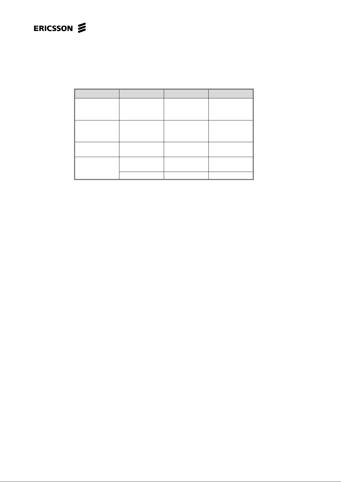
Table 5.1shows the limits for the VCXO measurements.
Parameter Min Max Unit
VCXO
Control at
DAC 00 Hex
VCXO
Control at
DAC 3FF Hex 13 67 ppm
VCXO
Control Range 40 80 ppm
Calibrated
VCXO 262 762 Dec
DAC 106 2FA Hex
-67 -13 ppm
Table 5.1
Trouble Shooting Guide, Advanced
5.3 How to find the fault
Open the phone and check for liquid damage.
Start the phone in the test program.
Start the transmitter in static mode at middle channel (699). Make sure that the transmitter locks.
Turn off t he modulation by selecting ”Mod off”.
Go to Misc /DAC Parameter.
Set TCXO to 00 Hex. Notice t hat the DAC value does not change until clicking at ”Close”.
Measure the DC voltage at C320 (0.3 V).
Set TCXO to 3FF Hex. Notice that the DAC value does not change until clicking at ”Close”.
Measure the DC voltage at C320 (2.9V).
If both voltages are correct, but any of the VCXO measurements are incorrect, the fault is
usually due to B301. Sometimes the fault is due to V302, C321, C322 or C323.
If both voltages are constantly too low, remove C320. Measure the voltages again.
If the voltages are correct now, the fault was a short circuit in the capacitor.
If the fault remains, it is usually due to N800,C853 or C854. (The voltage at C853 and C854
should be 1.1V)
If both voltages are equal, but not 0 V, the fault is almost always due to N800.
If both voltages are correct, but the V CXO calibration is incorrect, the fault i s usually due to
B301 or V302. Sometimes it is due to C321, C322 or C323.
VCXO faults can be due to N202, but that is not very common.
4/00021-3/00021/16 C 21(102)
Page 22
Trouble Shooting Guide, Advanced
You can verify that the fault is gone by measuring the output frequency of the transmitter with
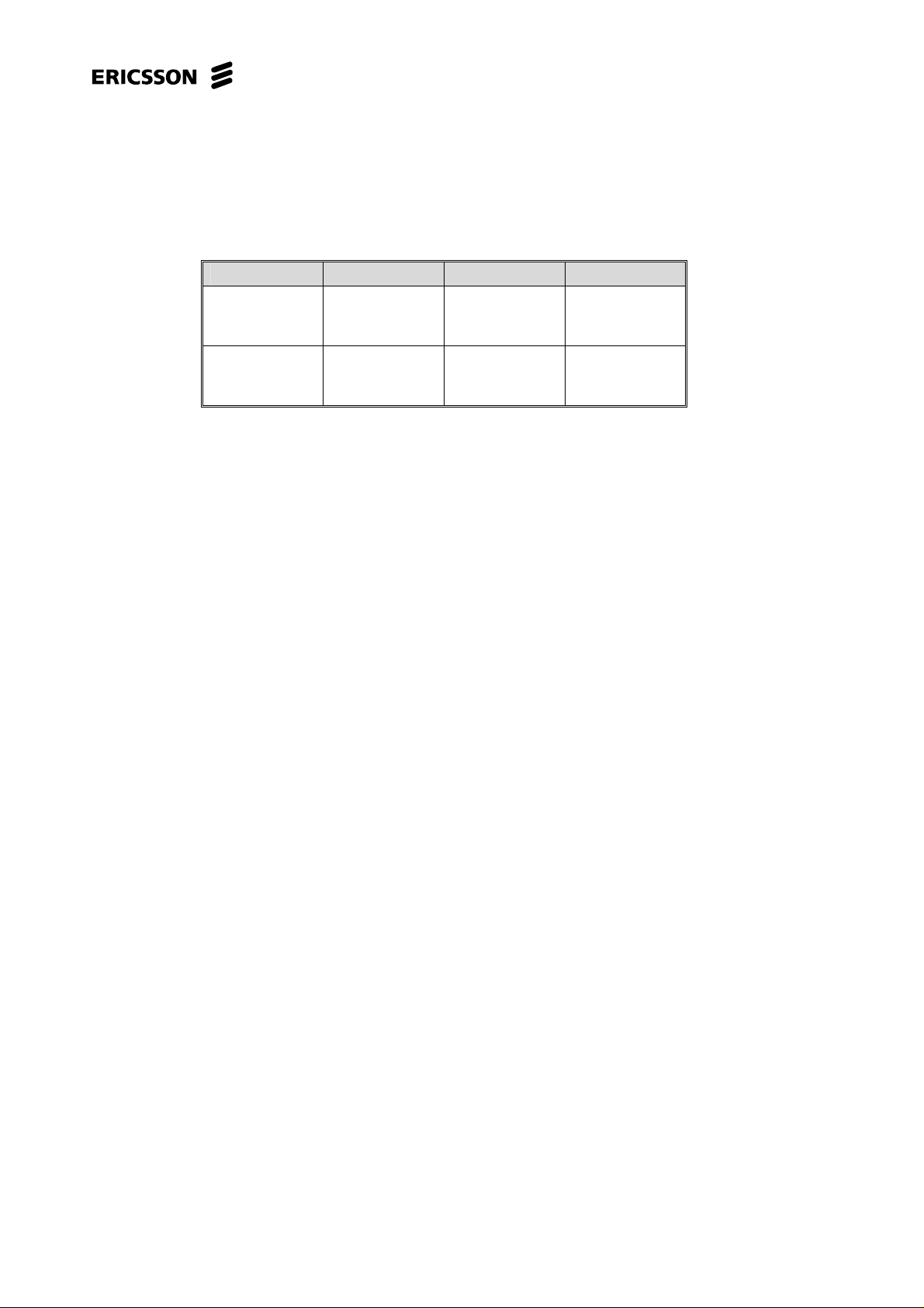
VCXO-DAC at 00 and 3FF Hex and compare the result with table 5.2.
Parameter Min Max Unit
VCXO
Control at
DAC 00 Hex 1747.4829 1747.5773 MHz
VCXO
Control at
DAC 3FF Hex 1747.6227 1747.7171 MHz
Table 5.2 (Applies for channel 699)
4/00021-3/00021/16 C 22(102)
Page 23

6 Calibration RSSI
6.1 What is RSSI
In the mobile phone, the received RF-signal strength is measured and indicated by a f unction
called RSSI, Received Signal Strength Indicator.
During a call in progress the phone measures the current signal strength sequentially from a
number of base stations ordered by the switch when setting up t he call. The measurement starts
at the base station serving cell and continues with the RF-signals of up to 6 surrounding base
stations. The measurement cycle is continually repeated.
The logic part of the phone then calculates a number of values of the received RF-signals and
reports the amplitude of the RF-signals from the different base station to the switch through a
logical channel.
The signal strength report is used in an evaluation process for Location and Handover, i.e. when
the switch evaluates the speech quality, signal strength and traffic parameters to be outside the
limit values of the current physical channel and chooses to start a new channel for the
connection. A physical channel is the combination of a timeslot (TS) and a radio channel
(ARFCN). The physical channel (TS/ARFCN) can be allocated to the current base station or any
of the surrounding base stations at handover.
Trouble Shooting Guide, Advanced
For the speech quality and the MS to Base distance, it is important that the reported
measurements of the RF-signal are correct and calibrated towards known values. If the reported
values are too high it results in late handovers and bad readability due to the limits that are set
out of reach for the MS. The opposite, t oo low values, provokes the switch to make unnecessary
handovers, increased traffic load and perhaps dropped calls by forced release.
The received signal carries information both in phase as well as amplitude. The phase contains
the digital information (speech and signalling data) and is detected in a phase digitizer for
further processing in the main program. The amplitude of the received signal is measured in
N800, giving a value called RSSI.
RSSI is used for two measurement functions, electrical and numerical (mean value and
momentary value). The electrical value of the RSSI is used to report the signal strength to the
switch through the base station as current Rx-level. The numerical RSSI-value is calculated and
only used internally in the phone by the DSP.
The RSSI measuring procedure is to compare the strength of the measured signals and compare
them to a calibrated scale of reference levels and point out the one closest to the current RFlevel. There are two scales, one for GSM900 and one for GSM1800, both are calibrated
separately. To create these scales, the MS is calibrated with known RF-signal levels from –
110dBm to –40dBm, with a 5dBm increment at a frequency in the Mid ARFCN range (ARFCN
62 is usually used as a mid channel for GSM900 and ARFCN 699 for GSM1800). This
procedure is called RSSI calibration.
These 15 RF-signal levels are digitized by the RSSI function and temporarily saved in the RAM
memory by a test program. The test program then performs an interpolation and calculates the
rest of the (up to 256) reference value positions and loads them into a part of the MS program
memory, EEPROM.
4/00021-3/00021/16 C 23(102)
Page 24

Every RF-signal level, that is processed by the RSSI-function, can now be presented in digital
form by reading the nearest corresponding reference level from the EE-PROM, with a resolution
of 16 bits, and sending it as current Rx-level information to the base station.
These reference l evels are unique for every phone since the signal path through every receiver is
dependent on unique parameter values. As, for instance, component tolerances, mounting,
soldering and so on. Every change, for instance a repair, an adjustment, a component being
soldered, a component ageing and so on, brings the possible need of a new calibration.
6.2 How to find the fault
The fault can be due to either an incorrect measurement of the RSSI value or too large losses in
the signal path. If the RSSI calibration is incorrect for only one frequency band, GSM900 or
GSM1800, the fault is usually in the signal path, see chapter 18 (Sensitivity and Rx-quality) for
a hint on where to troubleshoot. To check the measurement of the RSSI value, only one of the
frequency bands is needed. We have used the GSM900 band.
Trouble Shooting Guide, Advanced
Set Rx-amplitude from GSM-test set to 947.4 MHz and -50 dBm. Use a modulated signal
(GMSK on).
Open the phone and check for liquid damage.
Attach the board to the fixture and start the test program.
Go to Radio/RSSI Measurement and make a RSSI measurement at channel 62.
If the RSSI value is about 0xC8, it is probably okay. But to be sure, measure at -100 dBm
(should be about 0x44).
If the RSSI value is 0x00 or 0xFF (for different signal strengths), the fault is usually due to
N800 or D600.
If the value is faulty, the problem is probably in N202, N800 or N300.
4/00021-3/00021/16 C 24(102)
Page 25

7 Power Level Calibration
7.1 Introduction
In the GSM 900 system, it is possible for a phone to transmit with 15 different power levels,
from 33 dBm (power level 5) to 5 dBm (power level 19). In the GSM1800 system, it is possible
for a phone to transmit with 16 different power levels, from 30 dBm (power level 0) to 0 dBm
(power level 15). It is best to transmit at as low output power as possible, but with maintained
transfer quality, in order to e.g. save current in the battery and restrict the disturbances. The base
station evaluates the transfer quality and informs the phone when to change the output power.
For the base station to be able to regulate the output power of the phone in a satisfying way, the
power levels of the phone have to be as the base station expect. This means that the power levels
of the phone have to be calibrated to be accurate enough.
Trouble Shooting Guide, Advanced
Fig 7.1 shows a very simplified schematic of the power regulation.
Fig. 7.1
The calibrated DAC values are stored in the EEPROM. When the base station orders the phone
to transmit at a certain power level, the DAC value for the current power level is taken from the
EEPROM and sent to the Power level-DAC in N800. The output voltage POWLEV of the DAC,
lets the power regulation of the radio know how large the power should be. N550 uses
POWLEV to create the control voltage VREG with Offset level and Full Power level.It
regulates the amplification of the power amplifier. The regulation is fed back by measuring the
current consumption of the power amplifier using R412. The signal is called VSENSE.
Table 7.1 (GSM900) and 7.2 (GSM1800) shows the allowed DAC values and the output power
goal of the calibration.
4/00021-3/00021/16 C 25(102)
Page 26
Trouble Shooting Guide, Advanced
Power
Level
Output
Power
(dBm)
5 32.5 ±0.3
6 30.5 ±0.3
7 29 ±0.5
8 27 ±0.5
9 25 ±0.5
10 23 ±0.5
11 21 ±0.7
12 19 ±0.7
13 17 ±0.7
14 15 ±0.5
15 13 ±0.5
16 11 ±0.5
17 9 ±0.5
18 7 ±0.5
19 5 ±0.5
Table 7.1 (GSM 900)
Power
Level
Output
Power
(dBm)
0 30 ±0.3
1 28 ±0.5
2 26 ±0.5
3 24 ±0.5
4 22 ±0.5
5 20 ±0.7
6 18 ±0.7
7 16 ±0.7
8 14 ±0.7
9 12 ±0.7
10 10 ±0.7
11 8 ±0.7
12 6 ±0.7
13 4 ±0.7
14 2 ±0.7
15 0 ±0.7
Table 7.2 (GSM1800)
4/00021-3/00021/16 C 26(102)
Page 27
The power calibration is a part of the radio calibration in EFRA. The calibration is performed in
15 steps, from the highest (5) to the lowest (19), for GSM900 and in 16 steps for GSM1800 (0-
15), one step for each power level. The computer controls the calibration by setting t he Power
level DAC for the phone at the current power level and checking the output power using a
spectrum analyser or a GSM test set. Default values are used as starting DAC values. The
computer changes the DAC value to attain the correct output power for the current power level.
The value is temporarily saved in the RAM of the phone. When the computer has attained the
right output power for each power level, the values for the power levels not in use are first
interpolated, then all DAC values are saved in the EEPROM. If the correct power is not
achieved or one of the DAC values is outside of the limits, then the calibration has failed and
nothing is written i n the EEPROM.
7.2 How to find the fault
If the power calibration failed or if the output power is several dBm too low, open the phone and
check for liquid damage.
Make sure that the antenna connector (W101) is okay.
Power up the board and start it in the test program.
Trouble Shooting Guide, Advanced
Measure the voltage at C833. If it is lower than approximately 1.5 V, replace the capacitor.
For GSM900:
Start the transmitter in switch mode at middle channel (62) and ”DAC 4 value” at FF. Check if
there is enough output power (30- 35 dBm) at the antenna plate using the spectrum analyser. We
have been using the following settings while measuring: CF- 902.4MHz, SPAN- 0 Hz, RBW300 kHz, VBW- 100 kHz and Sweep- 0.8 ms.
If the output power is correct, the fault can be due to the frame. The fault can also be due to a
change in the characteristics in some of the components, participating in the power regulation,
because of ageing. For some power levels this can make the output power or the DAC values
ending up outside the limits. In that case, the fault is usually due to N400 or N550. The fault can
also be due to N800, N390 or D600.
If the output power is too low, measure the control voltage POWLEV at N550:10 using an
oscilloscope. It should l ook like in Fig 7.2.
Fig. 7.2
4/00021-3/00021/16 C 27(102)
Page 28

Trouble Shooting Guide, Advanced
If the control voltage is too low, the fault is usually due to N800. It can also be due to D600.
If the control voltage is correct, measure VREG at N550:16 or N400:4 (type 2 PA 3.5 V, same
frequency), N400:7(Type 1 PA).
If VREG is too low, the fault is probably due to N550 or N400.
If VREG is correct, measure the signal Tx at N390:6 (10 dBm).
If the signal Tx is correct at N390:6, check the output power from N400:16 (Type 2 PA28
dBm), N400:4 (Type 1 PA 31 dBm).
If the output power is too low, replace N400.
If the output power is correct at N400 but low or missing at the antenna connector, the fault is
probably due to N203.
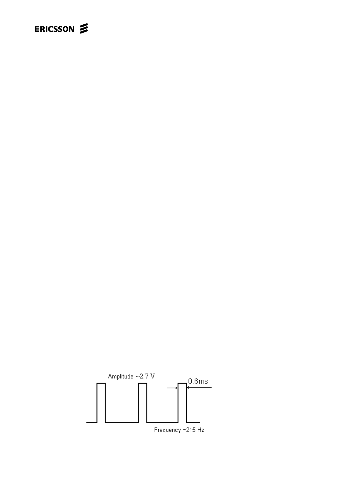
If the signal Tx is too low at N390:6, measure the feed voltage at N390:3 using an oscilloscope
(3.8 V, 215 Hz).
If the feed voltage is correct, the fault is usually due to N390 or N400.
If the feed voltage is incorrect, the fault is usually due to V350 or V351. Make sure that VRAD
is okay.
For GSM1800:
Start the transmitter in switch mode at middle channel (699) and ”DAC 4 value” at FF. Check if
there is enough output power (28- 32 dBm) at the antenna plate using the spectrum analyser. We
have been using the following settings while measuring: CF- 1747.6MHz, SPAN- 0 Hz, RBW300 kHz, VBW- 100 kHz and Sweep- 0.8 ms.
If the output power is correct, the fault can be due to the frame. The fault can also be due to a
change in the characteristics in some of the components, participating in the power regulation,
because of ageing. For some power levels this can make the output power or the DAC values
ending up outside the limits. In that case, the fault is usually due to N400 or N550. The fault can
also be due to N800, N390 or D600.
If the output power is too low, measure the control voltage POWLEV at N550:10 using an
oscilloscope. It should l ook like in Fig 7.2.
If the control voltage is too low, the fault is usually due to N800. It can also be due to D600.
If the control voltage is correct, measure VREG at N550:16 or N400:4 (type 2 PA 3.5 V, same
frequency), N400:7(Type 1 PA).
If VREG is too low, the fault is probably due to N550 or N400.
If VREG is correct, measure the signal Tx at N390:6 (13 dBm).
If the signal Tx is correct at N390:6, check the output power from N400:26(Type 2 PA31 dBm),
C408 (Type 1 PA 28 dBm).
If the output power is too low, replace N400.
If the output power is correct at N400 but low or missing at the antenna connector, the fault is
probably due to N203.
If the signal Tx is too low at N390:6, measure the feed voltage at N390:3 using an oscilloscope
(3.8 V, 215 Hz).
4/00021-3/00021/16 C 28(102)
Page 29

Trouble Shooting Guide, Advanced
If the feed voltage is correct, the fault is usually due to N390 or N400.
If the feed voltage is incorrect, the fault is usually due to V350 or V351. Make sure that VRAD
is okay.
All the mentioned signal strength levels are approximate, especially when measuring at the
signal before the power amplifier, since the output power of the power amplifier radiates back
to the probe. You have to consider this when comparing your values with a reference.
4/00021-3/00021/16 C 29(102)
Page 30
8 Intermediate Power Calibration
8.1 What is intermediate power
Intermediate Power is a calibration necessary to do to fulfil the demands of the GSMspecification for the up- and down-ramping of the power and to minimize the transient spectra.
The up- and down-ramping of the control voltage of the power amplifier does not change
momentarily from zero-to-max/max-to-zero. That would cause a large number of over tones due
to the switch. The up- and down-ramping of the control voltage are i nstead performed with two
help steps. The control voltage then passes through an exponential amplifier and a Bessel low
pass filter in N550 where the transient disturbance is reduced. This gives a control voltage
without the straight, vertical edges and the sharp corners that produces the over tones. The two
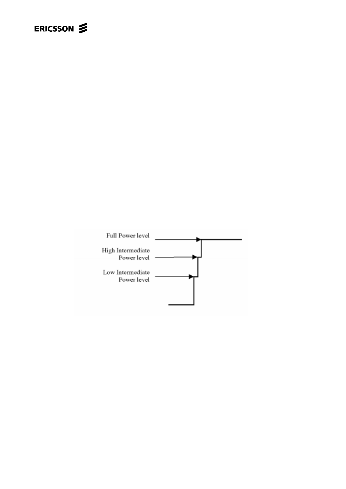
help steps in the up- and down-ramping of the power are called Intermediate Power level.
Trouble Shooting Guide, Advanced
The figure below shows the up-ramping of the control voltage before it passes through the
exponential amplifier and the low pass filter, i.e. what the up-ramping steps looks like.
Fig. 8.1
The three power steps Low Intermediate Power level, High Intermediate Power level and Full
Power level are set by the power level DAC in N800 and are amplified and filtrated in N550.
Low and High Intermediate Power level uses default values to generate the voltage.
Fullpowerlevel(5–19forGSM900and0–15forGSM1800) is calibrated so that the Power
levels are correct according to the GSM – specification.
Intermediate Power level is calculated at the power calibration and is not shown in the test
protocol.
4/00021-3/00021/16 C 30(102)
Page 31

Trouble Shooting Guide, Advanced
9 Transient Spectrum (Spectrum due to Switching)
9.1 What is transient spectrum
In the GSM-system is all communication between the base station and the phone done switched,
in shape of bursts. The burst is a squared output power pulse with step up- and down-ramping.
Every time the voltage of the squared pulse changes rapidly there will be formed a number of
over tones. The over tones have got different frequencies and amplitudes. The amount of over
tones and what amplitude they have got depends on how steep the up- and down-ramping is, the
higher up- and down-ramping, the higher amplitude and frequency of the over tone. The over
tones form a spectrum that is called transient spectrum or ”Spectrum due to switching”.
To be able to get lower amplitudes for the over tones in the transient spectrum, the up- and
down-ramping does not change momentarily from zero-to-max/max-to-zero. Instead this is done
with two help steps, these two help steps are called Low and High Intermediate Power level.
The figure below shows what the control signal POWLEV from N800 (DAC 2) looks like. The
times in the figure are approximate measured at an approved phone at full Power level.
Fig. 9.1
The control voltage POWLEV then passes through an exponential amplifier and a Bessel low
pass filter in N550 where the transient disturbance is reduced. This gives a control voltage
without the straight, vertical edges and the sharp corners that produces the over tones. The
amplified and filtrated control voltage is called VREG and looks like the figure below.
4/00021-3/00021/16 C 31(102)
Page 32

Trouble Shooting Guide, Advanced
70 300 25 543 35 t (µs)
Fig. 9.2
The actual up- and down-ramping are much shorter then other parts of the control voltage.
Therefore it is only the up- and down-ramping in the figure that is timely proportional to each
other. The proportion for the amplitude is correct at Power level 5 (for GSM900) and Power
level 0 (for GSM1800).
The Zero Power level is a voltage level from the DAC that assures no output power at all. The
Offset level is the highest possible voltage before the power amplifier starts to transmit. The
Offset voltage compensates for the differences of voltage fault between different power
amplifiers and is produced in N550.
The tables below show the limits for maximum power levels at transient disturbances.
GSM 900
Parameter Min Normal Max Units
Fc +400 kHz - - -19 dBm
Fc -400 kHz - - -19 dBm
Table 9.1
GSM 1800
Parameter Min Normal Max Unit
Fc +400 kHz - - -22 dBm
Fc -400 kHz - - -22 dBm
Table 9.2
”Measure Transient Spectra” is a part of the radio calibration in EFRA. It is performed after the
power calibration and measures the power levels at the middle channel frequency (± 400 kHz)
of the t ransmitter. The power level must not be higher then –19 dBm for GSM900 and –22 dBm
for GSM1800.
4/00021-3/00021/16 C 32(102)
Page 33

Trouble Shooting Guide, Advanced
9.2 How to measure the transient spectrum
GSM900:
Power up the board and start it in the test program.
Start the transmitter in switched mode at channel 64 and power level 5.
(Before performing a transient spectrum measurement you have to make sure that the spectrum
analyser has got the correct amplitude compensation. To do this you use a phone with a known
output power and start the transmitter in static mode at power level 5. Then you compensate the
spectrum analyser until the correct output power is achieved. Convenient settings for this are:
CF – 902.8 MHz, SPAN – 0 MHz, RBW – 300 kHz, VBW – 100 kHz and SWEEP – 0.8ms.)
One method to measure the transient spectrum is to use the following settings at the spectrum
analyser: CF – 903.2 MHz, SPAN – 0 MHZ, RBW – 30 kHz, VBW – 100 kHz and SWEEP – 6
ms. You measure the highest level of the signal. The easiest way t o do it is to use ”single
sweep” to freeze the picture and ”peak search” to find the highest level. The spectrum should
look like the figure below.
Fig. 9.3
For the example in the picture we have measured the transient spectrum at channel 64 + 400
kHz. Do the same measurement at channel 64 - 400 kHz, by changing CF at the spectrum
analyser to 902,4 MHz. The power level must be inside the limits, i.e. lower then -19 dBm, for
both frequencies.
It is very difficult to make an exact transient spectrum measurement on a trouble-shooting site
since there are a lot of disturbances in the air. It can be a difference of a few dBm compared to
the measurement in EFRA.
4/00021-3/00021/16 C 33(102)
Page 34

GSM1800:
Same as for GSM900, but do not forget to change to GSM1800 and Power level 0 in the test
program, also change CF at the spectrum analyser. The Power level must be inside the limits,
i.e. lower than –22 dBm, for both frequencies.
9.3 How to find the fault
The fault is usually due to too low amplification in the power amplifier. When the amplification
in the power amplifier is lower then normal, but still high enough for the phone to pass the
power level calibration, the power amplifier is working at its maximum limit. This can result in
over tones in the shape of distortion.
The fault can also be due to a fault in the up- and down-ramping or one of the synths producing
over tones.
Trouble Shooting Guide, Advanced
You must start the phone in the test program and activate t he transmitter in static mode at full
Power level.
Check the control voltage VREG at N550:16 or N400:4 (type 2 PA 3.5 V, same frequency),
N400:7(Type 1 PA) using the oscilloscope. It should look like in the Fig. 9.4. Note t hat the
sweep time are different in the upper picture compared to lower pictures (the upper picture 0.2
ms/square and the lower pictures 10µs/square). We have been using a 10 times-probe, which
means that the amplitude are 10 times higher in the reality compared to what the picture is
showing (500 mV/square in stead of 50 mV).
4/00021-3/00021/16 C 34(102)
Page 35

Trouble Shooting Guide, Advanced
Fig. 9.4
If the up- and down-rampinglooks like the pictures above, the fault almost always is due to
distortion caused by the power amplifier. Replace N400 and do a new radio calibration. The few
times the fault are not due to N400 it is usually N390.
If the up- and down-rampingdoes not look like the pictures, the fault can be due to the
exponential amplifier, the low pass filter or the offset voltage. All three of the parts are
functions in N550.
If the offset voltage is too low, the fault is probably due to N550.
If the offset voltage is too high, the fault is probably due to C564. When C564 is faulty, it can be
difficult to calibrate the lowest power levels.
If the up- and down-ramping is steeper and/or there is a large curve in the middle of the
ramping, it is the low pass filter or the exponential amplifier that is faulty. The fault is due to
C561, C562 or N550.
If the up- and down-rampingis considerably shorter than in the pictures, the fault is due to
either C560 or N550. When C560 is faulty, it can be difficult to calibrate the lowest power
levels.
4/00021-3/00021/16 C 35(102)
Page 36

Trouble Shooting Guide, Advanced
10 Modulation Spectrum Switched Mode
(Spectrum due to Modulation)
10.1 Introduction
10.1.1 Description
In the GSM system the mobile phone (MS) transmitter ( Tx) output RF- signal is time-shared,
according to the principle of TDMA. This implies the transmitter to be STARTED exactly at a
controlled point of time to reach a specific RF-powerlevel within a very short and clearly
defined period of time < 28 µS. This RF-power levelshift, called upramp, must be as smooth
and linear as possible during t he transition low to high, in order to limit the spectral propagation.
The controlfunction for this levelshift is accordingly preprogrammed in three steps, each of
which is smoothed i n a digital function of a besselfilter.
When the transmitter is up at the decided RF-powerlevel, it is ready to send the message in a
digital burstformat. The message must be fully completed during a clearly defined period on the
timeaxis. Two different time interval exist. It is during this interval, the real significant message
is going to be sent. Some of the messages are system information only and some are digital
speech frames. But mostly both types in the same data packet. The method chosen for the
transmission via the transmitter carrier is decided to be GMSK digital modulation. Also during
this time interval, the spectral propagation must be limited within a specified bandwidth for the
system. Because of that limitation, there will be a compromise between readability / penetration
and the available frequency band. More about this in section 10.1.3.
After hopefully a completed message time-lapse, the transmitter shall be ST OPPED exactly at a
controlled point of time, to return to RF-off level again, within a very short and clearly defined
period of time <28µS. The transmitter RF-powerlevel downshift is called downramp and also
this must be as smooth and linear as possible during the transition from high to low, in order to
limit the spectral propagation. Same control functionality, as in the previous upramp, over three
steps and a besselfilter, is also utilized for the downramp.
The transmitter RF-powerlevel as a function of time can be seen in Fig 10.1.
4/00021-3/00021/16 C 36(102)
Page 37

(**)
+4
+1
-1
-6
-30
(***)
Trouble Shooting Guide, Advanced
dB
(*)
8µs 10µs 10µs 8µs
10 µs
(147 bits)
7056/13 (542.8) µs
10 µs
Fig. 10.1
Time mask for normal duration burst 147 bits 542.8 µS. There is also a shorter accessburst 87
bits 321.2 µS. (not present). Both have the same time period-length for the RF-levelshift.
According to the principle of TDMA and the burst nature of the signal, the output RF spectrum
results from two effects:
the RF-power levelshift at upramp and downramp. Designated: Spectrum due to Switching
transients.
the digital modulation process. Designated: Spectrum due to the Modulation and wide band
noise.
10.1.2 Consequences in spectrum and testing
In digital TDMA-systems as GSM 900 -1800 -1900 the transmitted RF-signal is repeated over
time, in a syncronuous timepattern. The active time intervals in the system, for the transmitter
and the receiver respectively, are called Timeslot (TS). In the system, the timeslots are allocated
on RF-carriers, in two frequency duplex at an Absolute Radio Frequency Channel Number
(ARFCN). This combination of time and frequency TS / ARFCN, is called a physical channel.
The system also has the ability to change the ARFCN each time the physical channel is opened,
in a programmable so called frequency hopping pattern controlled by the switch.
t
The MS consequently has the ability to syncronuous follow the physical channel,bothinthe
time-domain and in the frequency-domain. Accordingly the MS timing functions are facing
specific demands, on precisely switching the transmitter and receiver up and downand for the
stability and rapid changing of RF-channel in the frequencygenerator. Due to this rapid RFlevelshift, in both the time- and fre quency-domain, unwanted spectrum components are
generated and occupying some space in the total spectrumdistribution, in excess to the
modulation from the wanted signal.
4/00021-3/00021/16 C 37(102)
Page 38

Trouble Shooting Guide, Advanced
Thetwoeffectsof,theRF-powerlevelshiftupramp / downramp and the digital modulation
respectively, are specified separately in GSM 11.10 and 11.20. The measurement method used
to analyse separately those two effects is based on the "ringing effect" during the transients and
is a measurement in the time domain, at each point in frequency.
In order to get a reliable testresult, the two effects must be separated in two different
measurements, which is possible thanks to the fact, they are separated in the time domain. This
will also put demands on the i nstruments, to have the feature of synchronising to the physical
channel TS / ARFCN, both in normalmode and hoppingmode. And in addition to that also
timegating, to make it possible to activate the measurement, between a START point and a
STOP point, i n the RF-signals time domain. So called Gated Measurements.
The effect of the RF-power levelshift, designated Spectrum due to switching transients, will then
be possible to separate from the total spectrum by setting the timegate closed and deactivate the
instrument for the time interval where switching is present. Gate closed, will exclude
measurement results from the instrument video screen.
By adaptation of START and STOP points in the time domain for Gated Measurements in
spectrum, it will be possible to analyse also this effect of switching. But, that is a measurement
not included in the scope of this description.
10.1.3 The actual RF-spectrum
When the MS has a call in progress, the transceiver is switching between receive / transmit, to
follow the physical channel according to the principle of T DMA. In the frequency domain
around the carrier ARFCN, the transmitter produces a RF-spectrum with an amplitude and
bandwidth depending on the Tx RF-power and the two effects of switching and modulation, as
we have learned from the previous description. The spectrum is spread over a wide frequency
band, but is technically limited by the equipment design and must conform within the GSM
spectrum mask.
To verify that the MS really conform to the spec GSM 11.10 it is tested over the frequency
band, at integer multiples of the channelseparation 200 kHz, on both sides of the carrier ARFCN
specified in a Method of test 13.4 and a Procedure. This test is rather complicated and time
consuming and is mandatory for design and production to fulfill the requirements for type
approval. But for testing at normal maintenance and repair, it is permitted to reduce the testand
simplify for economical reasons, at a reasonable l evel.
With a Spectrum Analyser set to zero span, resolution bandwidth 30 kHz, peak hold and video
bandwidth 100 kHz, it is possible to catch a narrow sample of the spectrum, as a time waveform
due to a transmitted burst. By repeating that sample over the time- and frequency - domains for
a long raw of consecutive bursts it will be possible to measure the average of the spectrum
components selected, in a timegated measurement. The example of such a time waveform as
seen in a 30 kHz RBW offset from the carrier, is given in Fig 10.2.
4/00021-3/00021/16 C 38(102)
Page 39

Trouble Shooting Guide, Advanced
Fig. 10.2
Note that in this time waveform spectrum components from both the switching and the
modulation are visible. Looking at the timeaxis we know that the transmitter is started before
the useful burst at the upramp. The instrument is time gated and the START point is set to the
beginning of the burst (0%).
At that part of the waveform the spectrum is still affected by the upramp and a peak of
switching transients is visible. The beginning of the time waveform is therefor not good for
measuring the modulation spectrum.
In the middle of the burst there is a training sequence usually called midamble, with an equal
bitpattern in every normal burst. This part is not interesting for modulation measurements either.
The part of the waveform that follows after the midamble, called the "Averaging period" in the
picture, is the part decided to be measured as the Spectrum due to the Modulation and wide
band noise by definition in the GSM spec. This period is finished at 90%, before the end of the
burst. This is to avoid interference from switching transients at the downramp.Attheendofthe
time waveform again spectrum components from the switching is present, because the timegated
measurement has got a STOP point at the end of the downramp period.
By setting the START- and STOP points to the appropriate timing around the specified period,
the modulation spectrum generated by at least 40 of the bits 87 to 132 is measured. The
spectrum analyser averages over the gated period and over 50 bursts when the MS is
commanded to its maximum power or 200 bursts at the minimum power level.
This measurement is referred to the GSM specification 05.05 s 4.2 Output RF spectrum.
4/00021-3/00021/16 C 39(102)
Page 40

Trouble Shooting Guide, Advanced
10.1.4 Spectrum due to the modulation and wide band noise
The telephone is connected to a test equipment: Fixture, Computer with a testprogram,
Communication T ester or a Spectrum Analyser and a Powersource. T he Tx is started at high
power level PL 5 in switched mode on an ARFCN in the Mid ARFCN range. At the same time
the Rx is switched OFF.
A specific designed base band signal for testing is generated by the testprogram and injected to
the Tx- modulator. The signal, only used for testing has a digital pattern combined from a
Pseudo Random Bit Sequence (PRBS) and Training Sequence (TSC nr 0). These are combined
in a burst with the two datafields filled with PRBS and TSC 0 as the midamble. The signal
pattern is designed to give a modulation spectrum, good for testing, that optimally uses the
channel bandwidth.
A gated measurement is performed with the Spectrum Analyser set to capture the whole useful
part of the burst, i.e. from 0% to 100% in Fig 10.2. No matter of the interference from switching
transients. Assumed to be negligible.
Each carrier is measured at the time. Beginning with the ARFCN here called Fc. An average of
the modulation power content in the spectrum on Fc is taken from 3 repeated bursts. The result
will be used as a reference level.
Two more measurements will be done at the adjacent RF-channels + 400kHz and - 400kHz
apart from the Fc. But still the Fc as the active modulated carrier. Equally an average of the
modulation power content in the spectrum on the adjacent RF-channel is taken from 3 repeated
bursts on each of the two RF-channels at the time. The two results from Fc+400kHz and Fc–
400kHz are compared to the result from Fc as a reference RF–power level in dBm.
When compared to the reference, each of the two adjacent RF-channels gets a lower value,
calculated as a difference in dBc down from the Fc. The smallest difference is the valid
measurement result. (Easiest to achieve, but closest to the limit).
This is the measurement result of Spectrum due to the Modulation and wide band noise and will
be examined according to the requirements specification in the doc 1524 TEST DATA written
and approved by the Ericsson Testengineering and based on the GSM specification.
The requirement is that the absolute RF levels in dBm and the levels in dBc relative to Fc, from
all three results must not exceed the limit of a modulation spectrum mask decided in the GSM
spec. Any crossing of this limit is considered as a failure.
4/00021-3/00021/16 C 40(102)
Page 41

10.2 How to find the fault
The ”Modulation Spectrum Switched Mode” is sometimes called ”Spectrum due to modulation”
or ”Switched Modspectra” and is a measurement in the radio calibration in EFRA. The
measurement is done at middle channel with the highest calibrated power level in switched
mode, Power level 5 for GSM900 and Power level 0 for GSM1800.
An average value over a number of bursts at carrier wave frequency (902.4 MHz for GSM900
and 1747.6 MHz for GSM1800) is calculated at first.
Then a new average value over some other bursts is calculated, but at a frequency +400 kHz
from the carrier wave frequency.
One more average value is calculated, now at a frequency –400 kHz from the carrier wave
frequency.
The level (+400 kHz or –400 kHz) with the most faulty value is reported as the measured value
related to the carrier wave amplitude.
Trouble Shooting Guide, Advanced
The measurement ”Modulation Spectrum Switched Mode” is very difficult to perform at a
trouble shooting bench. Since you only measure at a part of the burst, between the up- and
down-ramping, it demands among other things a special trig. You calculate the average value by
measuring at a number of bursts at the chosen part. You can measure at correct number of
bursts, trig in the correct way (measure at correct part of the burst), calculate the average value
and finally relate the value to the output power using a computer (and the appropriate software).
But since you do not have access to computer controlled instrument when trouble shooting, you
have to use indirect measuring methods, for example checking the static spectra.
A ”Modulation Spectrum Switched Mode”- fault usually occurs together with a ”Transient
Spectra”-fault. Such a fault is usually due to a fault in the up- and down-ramping. If this is the
case, start trouble shooting according to chapter 9 (”Transient spectrum”).
The fault is usually due to too low amplification in the power amplifier. When the amplification
is lower then normal, but still high enough for the phone to pass the Power Level Calibration,
the power amplifier is working at its maximum limit. This can result in over tones in the shape
of distortion. The fault can also be due to noise at one of the feed voltages of the radio or an
appearance of unwanted frequencies (e.g. noise) in the output signal.
Open the phone and check for liquid damage.
Start the phone in the test program.
Start the transmitter of the phone in static mode, without modulation, at channel 62 for GSM900
or channel 699 for GSM1800.
NOTE! If the card is type 2, remember to use the negative bias voltage when changing to
static Tx mode.
Compare the spectrum with the one of a working phone. Make sure that the level of the noise is
not higher than for a working phone. Sometimes the level of the noise is low, but wide banded.
To be able to find the noise during such circumstances you have to check the spectrum at both 1
MHz and 10 MHz SPAN.
4/00021-3/00021/16 C 41(102)
Page 42

Trouble Shooting Guide, Advanced
The settings for the spectrum analyser are, for GSM900: CF- 902.4 MHz, RBW- 10 kHz, VBW10 kHz, Sweep- 30 ms and SPAN 1 MHz, respectively 10 MHz. For GSM1800: CF- 1747.6
MHz, RBW- 10 kHz, VBW- 10 kHz, Sweep- 30 ms and SPAN 1 MHz, respectively 10 MHz.
The spectra should look like the figures below.
1 MHz SPAN, no modulation
Fig. 10.3
10 MHz SPAN, no modulation
Fig. 10.4
4/00021-3/00021/16 C 42(102)
Page 43

10 MHz SPAN, no modulation
Wide banded noise
Trouble Shooting Guide, Advanced
Fig. 10.5
Turn the modulation on.
Compare the inter modulation products with the one of a working phone. They must not be too
high.
A normal spectrum with modulation should look like the figure below.
1 MHz SPAN, modulation set on
Correct spectrum
Fig. 10.6
If there is noise in the spectrum, the fault can be due to noise in one of the feed voltages,
VRAD, VVCO or maybe VDIG. Noise can be due to e.g. ageing filter capacitors (usually the
electrolytes) or deteriorated performance in the voltage regulators of the radio. If you have got a
really good oscilloscope, it is possible to measure the noise. Noise in the spectrum can also
come from the synths, either in the PLL-circuit N300, N202 or in one of the VCO’s.
4/00021-3/00021/16 C 43(102)
Page 44

Trouble Shooting Guide, Advanced
If the inter modulation products have not got the right level, proceed to chapter 3 (”Calibration
IQ”-fault).
If the static spectrum looks correct, the fault most certainly is due to the power amplifier, N400.
Replace the power amplifier and perform a new radio calibration.
If the radio calibration succeeded, the fault was due to the power amplifier.
If the radio calibration failed, the fault can be due to noise in one of the feed voltages VRAD,
VVCO or VDIG. Noise can be due to e.g. ageing filter capacitors (usually the electrolytes) or
deteriorated performance in the voltage regulators of the radio.
4/00021-3/00021/16 C 44(102)
Page 45

11 EE-prom
11.1 Write to EE-prom
Large amount of data is stored in the RAM memory of the phone during the radio calibration in
EFRA. This information is stored permanently in a 16 kB large EE-prom after interpolation.
The data transfer is done serially at an I
I2CDAT for data and I2CCLK for clocking. (The I
The figure below shows a schematic over the data transfer.
Trouble Shooting Guide, Advanced
2
C-bus (Inter IC). The I2C-bus consists of two lines,
2
C -bus also goes to the display).
11.2 How to find the fault
There is a possibility, in the trouble shooting part of EFRA, to test the communication and a
limited part of t he function in the self test. The functionality test that is done is the processor
writing and reading at a few addresses. If the self test shows w”Check EEProm Failed”, the
phone is faulty, but the self test does not display all faults, so there is a possibility for the self
test not to detect the fault.
Open the phone and check for liquid damage.
Check the soldering at D600:3, 4.
Check R619, R620.
Make sure that there is not a short circuit against ground at I2CCLK or I2CDAT (usually at the
display).
Power up the board and check VDIG (3.2 V).
Mostly it is D630 that is broken (cannot be replaced), but sometimes the fault can also be due to
D600.
Fig. 11.1
4/00021-3/00021/16 C 45(102)
Page 46

Trouble Shooting Guide, Advanced
12 ADC Calibration (Voltage Calibration)
12.1 What is ADC calibration
For the processor to be able to control t he phone in a correct way it has to know the current
battery voltage. The battery voltage is measured using N550 and N800. N550 compares VBATT
and VRAD according to the formula below. The result of the comparison is presented as an
analogue voltage VTRACK.
0.85
(VBATT – VRAD) = VTRACK
*
Since the processor needs the information presented in digital form, VTRACK is transformed in
an ADC in N800. To make the measurement of the battery voltage precise it is necessary to
perform a calibration. The calibration is performed at two voltages (4.5 V and 6.5 V). The
corresponding ADC-values are stored in the EEPROM. The ADC-values for other battery
voltages are produced by interpolation of the two calibrated voltages.
12.2 How to perform an ADC calibration
Start the phone in the testprogram.
Go to Logic\ ADC Calibrate.
When you have started ADC Calibrate following window is shown, telling you to set the battery
voltage on the power supply to 6.5V. When you have done that, click on OK.
Fig. 12.1
A new window shows up, telling you to change the battery voltage to 4.5 V on the power
supply. When you have done that, click on OK.
4/00021-3/00021/16 C 46(102)
Page 47

Trouble Shooting Guide, Advanced
Fig. 12.2
The result is shown in two windows, first ”High ADC calibration” (6.5V) and then ”Low ADC
calibration” (4.5V).
Fig. 12.3
Fig. 12.4
Table 12.1. shows the limits for the ADC-values at the calibration. When calibrating there must
be an accuracy of +
15 mV.
Battery voltage min max
6.5 V D2 FF hex
210 255 dec
4.5 V 32 5F hex
50 95 dec
Table 12.1
4/00021-3/00021/16 C 47(102)
Page 48

12.3 How to find the fault
Start the phone in the test program.
Set the battery voltage at 6.5 V.
Measure the exact voltage at VBATT (N550:18) and VRAD (N550:7).
Use the formula in section 12.1 to calculate VTRACK.
Example: VBATT= 6.5 V, VRAD= 3.8 V gives VTRACK 2.3 V
Measure VTRACK on N550:2.
If VTRACK is incorrect, it is due to the feed voltage VRAD or N550.
If VTRACK is correct, go to Logic\Read ADC. Read the value for VTRACK.
Trouble Shooting Guide, Advanced
If both the voltage VTRACK and t he ADC-value are correct there is probably nothing wrong
with the phone. Calibrate again.
If only the ADC-value is incorrect, it is usually due to the feed voltage VDIG or N800 and
sometimes D600.
4/00021-3/00021/16 C 48(102)
Page 49

13 Current Calibration
13.1 What is current calibration
A simplified diagram for the regulation of the charging current is shown below.
Trouble Shooting Guide, Advanced
Fig. 13.1
The information about the charging current is achieved by measuring the potential drop over the
resistor R553. This potential drop is then transformed in N550 to an analogue voltage, IMEAS.
Since the processor needs the information in digital form, IMEAS has to pass trough an ADC in
N800 on the way to the processor. This information lets the processor know how large the
charging voltage is at the moment and adjusts it, using the digital control signal ICONT. The
signal ICONT is transformed to the signal CH_SW in N550, with which the transistor V450 is
opened and closed.
The processor supervises the charging, using IMEAS to be able to have the average charging
current at a constant level, during the charging time.
For the adjusting to be exact, you need to calibrate the charging current. The calibration is
performed in two steps:
1. Zero current calibration – Measuring the level on IMEAS when there is no charger
connected, i.e. DCIO open.
2. High current calibration – The same measuring as above, but with DCIO high, and set on a
certain voltage and current limitation.
4/00021-3/00021/16 C 49(102)
Page 50

13.2 How to perform a current calibration
Start the phone in the test program.
Go to Logic \Current calibration.
When you start the Current calibration, the window below is shown telling you to set the battery
voltage for dummy battery to 5.8 V at the power supply and keep DCIO open. When you have
done that, click on OK.
Trouble Shooting Guide, Advanced
Fig. 13.2
The next window shows the result of the calibration.
Fig. 13.3
A new window is shown telling you to keep the battery voltage at 5.8 V and set the DCIOvoltage on the power supply at 6.8 V with the current limit at 800 mA. Use the same power
supply if it is possible to set two different voltages, otherwise use two power supplies.
One way to connect DCIO to the phone is to cut a cable from a battery charger and connect it to
the power supplier.
4/00021-3/00021/16 C 50(102)
Page 51

Trouble Shooting Guide, Advanced
Fig. 13.4
The result is shown in two windows, fast calibration and slow calibration. The fast calibration
is performed after 10-40 ms and verifies that C552 is mounted. The slow calibration is
performed after 350 ms and is the real calibration.
Fig. 13.5
Fig. 13.6
The limits for the calibrations are displayed in the table below
Type of
calibration min max dec / hex
Zero calibration 23 65 dec
17 41 hex
High current - Fast 10 98 dec
0A 62 hex
High current - Slow 101 166 dec
65 A6 hex
Table 13.1
4/00021-3/00021/16 C 51(102)
Page 52

13.3 How to find the fault
The fault can be in either the current measuring or the logical part/the AD-transforming. You
can find out which part is broken by measuring IMEAS and ICONT.
Start the board in the test program.
Set the battery voltage at 4.8 V.
Set DCIO at 6.8 V, but do not connect the DCIO-voltage to the phone.
Measure IMEAS on N550:3 (0 V).
Go to Logic \ Logic/SIM.
Set ICTRL high by pressing ICTRL.
Measure IMEAS again (0.4 V).
Turn off ICTRL.
If the voltage is incorrect, the fault can be due to R553, VRAD or N550.
Connect DCIO to the system connector.
Set ICTRL high.
Measure IMEAS (It varies from 0.4 V to 1.5V).
Trouble Shooting Guide, Advanced
Set ICTRL low.
If the voltage IMEAS is too high, the fault is usually due to R553 or N550, but sometimes also
N800.
If the voltage IMEAS is t oo low, measure the resistance of V450:1 - V450:4
If the resistance is 0 ohm, there is a short circuit in V450.
If the resistance is correct (high ), start the board in the test program and check VRAD.
If VRAD is too low, the fault is probably due to N550, N580 or a short circuit in one of the
components fed by VRAD.
If VRAD is correct, set ICTRL high again and measure the voltage on V450:3 (0 V ).
If the voltage on V450:3 is too high, measure ICONT on N550:24 (3.2 V).
If ICONT is missing, the fault is probably due to D600.
If ICONT is correct but the voltage on V450:3 is incorrect, the fault is due to N550.
If IMEAS and ICONT are correct, the fault is in the AD-transforming, but first measure the
resistance between AGND- J602:4 and GND- J602:10 (0 ohm).
If the resistance is too high, there is a foil damage and the board is not repairable.
If the resistance is correct, the fault usually depends on the feed voltage VDIG or N800, but
sometimes on D600.
4/00021-3/00021/16 C 52(102)
Page 53

14 Network Problems
14.1 Find out if the fault is related to Rx or Tx
Connect the phone to a GSM test instrument. GSM test set must be set as active base station and
use a test SIM for best result.
Attach a dummy battery and an antenna cable. Start the test program.
Go to: MISC \ Go to call processing.
Try to get serv at - 68.5 dBm input signal.
If the phone cannot get serv, proceed to section 14.2.
If the phone can get serv, proceed to section 14.3.
14.2 The phone cannot get serv
Trouble Shooting Guide, Advanced
If the phone cannot get serv, then the fault is probably somewhere in the LO-part or the losses in
the signal path are too large.
Open the phone and check for liquid damage.
Attach the board to the fixture and start the test program.
If you want to continue to trouble-shoot after signal test, perform “Reset MS” as follow:
1. Cut the battery voltage to the phone.
2. Set the battery voltage again.
3. Start the phone using a pulse on DCIO or the On/Off button.
4. Click on “Reset MS”. It will occur a message window that tells you to start the phone. Click
on OK.
5. The test program is running again.
For GSM900: Set Radio in Rx Static mode on channel 62.
Set Rx amplitude from the GSM test set to 947.4 MHz and -50 dBm.
Make sure that the Rx amplitude really is what it should be at the antenna plate using a spectrum
analyser. Increase or decrease the amplitude on the GSM- test set if necessary. We have been
using the following settings on the spectrum analyser when measuring the transmitter: CF-
947.4 MHz, SPAN- 1 MHz, RBW- 10 kHz, VBW- 10 kHz and Sweep- 30 ms.
For GSM1800: Set Radio in Rx Static mode on channel 699.
Set Rx amplitude from the GSM test set to 1842.6 MHz and -50 dBm.
Make sure that the Rx amplitude really is what it should be at the antenna plate using a spectrum
analyser. Increase or decrease the amplitude on the GSM- test set if necessary. We have been
using the following settings on the spectrum analyser when measuring the transmitter: CF-
1842.6 MHz, SPAN- 1 MHz, RBW- 10 kHz, VBW- 10 kHz and Sweep- 30 ms.
4/00021-3/00021/16 C 53(102)
Page 54

14.2.1 Fault in the LO
For GSM900: Change CF on the spectrum analyser to 947.4 MHz and increase the SPAN t o
200 MHz.
Measure frequency and amplitude on the local oscillator at N331:1 (947.4 MHz, 0 dBm).
If the LO signal is correct there are either too large losses in the signal path, a phase error or a
logical fault. Proceed to section 14.2.2.
If the frequency is correct, but the amplitude is too low, check the feed voltage on N331:7 (3.7
V).
If the voltage is correct, replace N331.
If the voltage is incorrect, check VVCO (3.8 V), SYNTON (3.2 V) and V337 with the
components that belongs to it.
If the amplitude is correct, but the frequency is incorrect, it is often due to N300. It can also be
due to N331 or D600.
If the signal is several MHz wide, replace C313.
Trouble Shooting Guide, Advanced
If the amplitude and the frequency is correct, decrease SPAN to 1 MHz and measure the LO
signal again. If there is noise on the signal, replace N300.
For GSM1800: Change CF on the spectrum analyser to 1842.6 MHz and increase the SPAN to
200 MHz.
Measure frequency and amplitude on the local oscillator at N330:1 (1842.6 MHz, 0 dBm).
If the frequency is correct, but the amplitude is too low, check the feed voltage on N330:7 (3.7
V).
If the voltage is correct, replace N330.
If the voltage is incorrect, check VVCO (3.8 V), SYNTON (3.2 V) and V338 with the
components that belongs to it.
If the amplitude is correct, but the frequency is incorrect, it is often due to N300. It can also be
due to N330 or D600.
If the signal is several MHz wide, replace C313.
If the amplitude and the frequency is correct, decrease SPAN to 1 MHz and measure the LO
signal again. If there is noise on the signal, replace N300.
If the LO signal is correct there are either too large losses in the signal path, a phase error or a
logical fault.
14.2.2 Too large losses in the signal path
For GSM900: Measure the signal at N203:5 (-53 dBm).
If the signal i s low, the fault is probably due to N203, C225, C227 or L203.
If the signal is missing, check that the pins on N203 has correct voltages (see table below)
N203 pin 2 pin 4 pin 8 pin 10
Rx 900/1800 0 V 3.8 V 3.8 V 0 V
Table 14.1
4/00021-3/00021/16 C 54(102)
Page 55

Trouble Shooting Guide, Advanced
If the values are correct, the fault is probably due to N203, C225, C227 or L203.
If any of the values are incorrect, there is probably a broken transistor, see schematics.
If the signal is correct at N203:5, continue measuring along the signal path.
At Z200:4 you should have -55 dBm and at Z200:6 -57 dBm.
At N202:10,11 you should have -56 - -58 dBm.
For GSM1800: The easiest point to first measure the signal is at Z201:1 (-54 dBm).
If the signal i s low, the fault is probably due to N203, C225, C227, L203 or Z201.
If the signal is missing, check that the pins on N203 has correct voltages (see table below)
N203 pin 2 pin 4 pin 8 pin 10
RxRx 900/1800 0 V 3.8 V 3.8 V 0 V
Table 14.2
If the values are correct, the fault is probably due to N203, C225, C227, L203 or Z201.
If any of the values are incorrect, there is probably a broken transistor, see schematics.
If the signal is correct at Z201:1, continue measuring along the signal path.
At N201:4,6 you should have -60 dBm.
At N202:7,8 you should have approximately the same.
14.2.3 Phase error or logical fault
For measuring phase error, go to Radio \ Sensitivity.
The RF-signal from the GSM test instrument must be non-modulated and the frequency must be
in accordance with the chosen channel.
For GSM900: At an input signal of -102 dBm, the phase error should be: PEAK 0-70, RMS 015 deg. The highest allowed frequency error is + 2000 Hz.
For GSM1800: At an input signal of -100 dBm should the phase error be: PEAK 0-70, RMS 015 deg. The highest allowed frequency error is + 2000 Hz.
When both the Peak phase error and the RMS phase error (sometimes even the frequency error)
are too large, it is usually due to a too large attenuation in the signal path.
When both the Peak phase error and the RMS phase error (sometimes even the frequency error)
are too large, but all the radio signals have correct amplitude and frequency, it can be due to
anyone of N800, D600 or N202.
When the Peak phase error is 1, the RMS phase error is 0 and the frequency error is 20000 Hz it
can be a frequency fault on B301 or a fault on N800.
4/00021-3/00021/16 C 55(102)
Page 56

Trouble Shooting Guide, Advanced
14.3 Connect a call against the instrument at power level 5
(GSM900) or power level 0 (GSM1800) and input signal -
68.5 dBm
If it works, proceed to section 24.4.
If it does not work, it is most likely a Tx related f ault.
If it only is at low channels on GSM900 you cannot connect a call, but you can at high channels
(GSM900) and at GSM1800, it is usually N390 that is faulty.
Open the phone and check for liquid damage.
Make sure that the antenna connector W101 is not mechanically damaged, unsoldered or dirty
(varnish, glue, oxide...).
Power up the board and start the test program.
Measure the voltage on C853 and C854(1.1 V). If the voltage is too low, replace the
corresponding capasitor.
For GSM900: Start the transmitter in static mode on channel 62 and check the transmitter’s
output power and frequency.
NOTE! If the card is type 2, remember to use the negative bias voltage when changing to
static Tx mode.
We have used the following settings on the spectrum analyser: CF- 902.4 MHz, SPAN- 200
MHz,RBW-10kHz,VBW-10kHzandSweep-30ms.
If the transmitter does not lock, first make sure that LO is working ( see chapter 14.2.1). If LO is
okay, but the transmitter still does not lock or have no output power measure the voltage on
N550:16 (VREG 1.2 V).
If VREG is too low, measure the signal POWLEV (1.45 V) on N550:10.
If the voltage POWLEV is too low, check the soldering at N800:61. If the soldering is correct,
the fault is usually due to N800. The fault can also be due to D600 or a short circuit in C853 or
C854.
If POWLEV is correct the fault is due to a break in R412 ( 0.1 ohm) (can be verified by
measuring the resistance between pin 17 and 18 on N550), N550, or a short circuit of the control
voltage VREG caused by N400.
If VREG is too high, measure the signal TXIN on C370 and C371( -10 dBm).Measure on both
sides of the capasitors to make sure that they are not broken.
If TXIN has got the right amplitude, check if there is a signal on R402 (Type 1 PA 3 dBm on
one side and 7 dBm on the other), N400:9 (Type 2 PA 0 dBm). If the signal is missing it can
depend on R400, R401, R402 or for type 2 cards D400. If the signal has got the right amplitude,
the fault depends on N400.
If the amplitude on TXIN is too low, measure the signal on N390:6 ( 9 dBm).
4/00021-3/00021/16 C 56(102)
Page 57

Trouble Shooting Guide, Advanced
If the signal on N390 has got the right amplitude, the fault probably depends on N391.
If the signal on N390 is missing, measure the feed voltage on N390:3 ( 3.7 V).
If he feed voltage is correct, the fault probably depends on N390 or BANDSEL is faulty.
If the feed voltage is incorrect, the fault usually depends on Z301, C350, C351, V350,V351 or
some of the following voltages are missing: VRAD or TXON. If TXON is missing, check
D600.
If VREG is correct, measure the signal TXIN on C370 and C371 ( -10 dBm).Measure on both
sides of the capasitors to make sure that they are not broken.
If TXIN has got the right amplitude, measure the signal at N400:4 (Type 1 PA 16 dBm),
N400:16 (Type 2 PA 12 dBm).
If the signal on N400:4 (Type 1 PA) ,N400:16 (Type 2 PA) is too low, the fault is probably due
to N400.
If the signal is too low at the antenna plate, the fault is probably the antenna switch
N203,V202,V203 or one of the associated components.
If the amplitude on TXIN is too low, the fault can depend on N391, C370 or C371.
If the transmitter locks, start the transmitter in switch mode on middle channel (62) with “DAC
4 value” on FF. Check if there is output power (30 - 35 dBm) at the antenna plate using the
spectrum analyser. We have used the following settings on the spectrum analyser: CF- 902.4
MHz, SPAN- 0 Hz, RBW- 300 kHz, VBW- 100 kHz and Sweep- 0.8 ms.
If there is no output power at all or i f it is too low, proceed to section 24.3.1.
If the output power is correct, proceed to section 24.3.2.
For GSM1800: Start the transmitter in static mode on channel 699 and check the transmitter’s
output power and frequency.
NOTE! If the card is type 2, remember to use the negative bias voltage when changing to
static Tx mode.
We have used the following settings on the spectrum analyser: CF- 1747.6 MHz, SPAN- 200
MHz,RBW-10kHz,VBW-10kHzandSweep-30ms.
Check the frequency of the transmitter (1747.6 MHz). If the frequency is misplaced, try to
decrease the “Adjust sweep current” until the frequency of the transmitter locks.
If the transmitter does not lock, first make sure that LO is working ( see chapter 14.2.1). If LO is
okay, but the transmitter still does not lock or have no output power, measure the voltage on
N550:16 (VREG 1.2 V).
If VREG is too low, measure the signal POWLEV (1.45 V) on N550:10.
If the voltage POWLEV is too low, check the soldering at N800:61. If the soldering is correct,
the fault is usually due to N800. The fault can also be due to D600 or a short circuit in C853 or
C854.
If POWLEV is correct the fault is due to a break in R412 ( 0.1 ohm) (can be verified by
measuring the resistance between pin 17 and 18 on N550), N550, or a short circuit of the control
voltage VREG caused by N400.
4/00021-3/00021/16 C 57(102)
Page 58

Trouble Shooting Guide, Advanced
If VREG is too high, measure the signal TXIN on C370 and C371( -9 dBm).Measure on both
sides of the capasitors to make sure that they are not broken.
If TXIN has got the right amplitude, check if there is a signal on R402 (Type 1 PA 4 dBm on
one side and 10 dBm on the other), N400:7 (Type 2 PA 8 dBm). If the signal is missing it can
depend on R400, R401, R402 or for type 2 cards D400. If the signal has got the right amplitude,
the fault depends on N400.
If the amplitude on TXIN is too low, measure the signal on N390:6 ( 12 dBm).
If the signal on N390 has got the right amplitude, the fault probably depends on N391.
If the signal on N390 is missing, measure the feed voltage on N390:3 ( 3.7 V).
If he feed voltage is correct, the fault probably depends on N390 or BANDSEL is faulty.
If the feed voltage is incorrect, the fault usually depends on Z301, C350, C351, V350,V351 or
some of the following voltages are missing: VRAD or TXON . If TXON is missing, check
D600.
If VREG is correct, measure the signal TXIN on C370 and C371 ( -9 dBm). Measure on both
sides of the capasitors to make sure that they are not broken.
If TXIN has got the right amplitude, measure the signal at N400:5 (Type 1 PA 20 dBm),
N400:26 (Type 2 PA) (14 dBm).
If the signal on N400:5 (Type 1 PA) ,N400:26 (Type 2 PA) is too low, the fault probably
depends on N400.
If the signal is too low at the antenna plate, the fault is probably the antenna switch
N203,V202,V203 or one of the associated components.
If the amplitude on TXIN is too low, the fault can depend on N391, C370 or C371.
If the transmitter locks, start the transmitter in switch mode on middle channel (699) with “DAC
4 value” on FF. Check if there is output power (28 - 32 dBm) at the antenna plate using the
spectrum analyser. We have used the following settings on the spectrum analyser: CF- 902.4
MHz, SPAN- 0 Hz, RBW- 300 kHz, VBW- 100 kHz and Sweep- 0.8 ms.
If there is no output power at all or i f it is too low, proceed to section 24.3.1.
If the output power is correct, proceed to section 24.3.2.
14.3.1 Low or no switched output power
For GSM900: Measure the control voltage POWLEV on N550:10 (Fig. 14.1) using an
oscilloscope.
Fig. 14.1
4/00021-3/00021/16 C 58(102)
Page 59

Trouble Shooting Guide, Advanced
If the control voltage is too low, check the soldering at N800:61. If the soldering is correct, the
fault usually depends on N800. It can also depend on D600 or a short circuit in C853 or C854.
If the control voltage is correct, measure VREG at N550:16 or N400:4 (type 2 PA 3.5 V, same
frequency), N400:7(Type 1 PA).
If VREG is too low, the fault is probably due to N550 or N400.
If VREG is correct, measure the signal Tx at N390:6 (9 dBm).
If the signal Tx is correct at N390:6, check the output power from N400:16 (Type 2 PA 28
dBm), N400:4 (Type 1 PA 31dBm).
If the output power is too low, replace N400.
If the output power is correct at N400 but low or missing at the antenna connector, the fault is
probably due to N203.
If the signal Tx is too low at N390:6, measure the feed voltage at N390:3 using an oscilloscope
(3.8 V, 215 Hz).
If the feed voltage is correct, the fault is usually due to N390 or N400.
If the feed voltage is incorrect, the fault is usually due to V350 or V351. Make sure that VRAD
is okay.
For GSM1800: Measure the control voltage POWLEV on N550:10 (Fig. 14.1) using an
oscilloscope.
If the control voltage is too low, check the soldering at N800:61. If the soldering is correct, the
fault usually depends on N800. It can also depend on D600 or a short circuit in C853 or C854.
If the control voltage is correct, measure VREG at N550:16 or N400:4 (type 2 PA 3.5 V, same
frequency), N400:7(Type 1 PA).
If VREG is too low, the fault is probably due to N550 or N400.
If VREG is correct, measure the signal Tx at N390:6 (11dBm).
If the signal Tx is correct at N390:6, check the output power from N400:26 (Type 2 PA 30
dBm), C408 (Type 1 PA 28 dBm).
If the output power is too low, replace N400.
If the output power is correct at N400 but low or missing at the antenna connector, the fault is
probably due to N203.
If the signal Tx is too low at N390:6, measure the feed voltage at N390:3 using an oscilloscope
(3.8 V, 215 Hz).
If the feed voltage is correct, the fault is usually due to N390 or N400.
If the feed voltage is incorrect, the fault is usually due to V350 or V351. Make sure that VRAD
is okay.
4/00021-3/00021/16 C 59(102)
Page 60

Trouble Shooting Guide, Advanced
All the mentioned signal strength levels are approximately, especially when measuring at the
signal before the power amplifier, since its output power radiates back to the probe. This has to
be considered when comparing measured values with reference values.
14.3.2 The switched output power is correct, but connecting a call is
not possible
Turn off switch Tx.
Set the spectrum analyser to: SPAN- 1 MHz, RBW- 10 kHz, VBW- 10 kHz, SWEEP- 30 ms.
Start the transmitter in static mode with modulation on the middle channel (62 for GSM900 and
699 for GSM 1800).
Make sure that the spectra look like the one in Fig. 14.2.
Fig. 14.2
If it looks like the one in the figure, but the phone cannot connect a call, is it a logical related
fault and usually depends on D600 or N800.
If the spectra does not look like the figure, it is either one of the modulation signals (MODQN,
MODQP, MODIN, MODIP) that is missing from D600 or a faulty low pass filter to the
modulation signals (R642, R643, R644, R645, C106 and C108). Measure with an oscilloscope
on the capacitors. The signals are sinus shaped with the frequency 67.7 kHz and amplitude 3.0
V. Compare the signals with each other. The fault is on the modulation signal that differs from
the others. If the modulation signals looks good and are in the right phase (90 degrades turned
compared to each other) then the fault could be caused by N202.
4/00021-3/00021/16 C 60(102)
Page 61

Trouble Shooting Guide, Advanced
14.4 Read the Rx level value from the instrument while the
call is still connected
If the Rx level value is at 40- 46 steps, make sure that the output power is 31-35 dBm (GSM900,
power level 5) or 28-32 dBm (GSM1800, power level 0).
If the value is correct there is probably nothing wrong with the phone.
Decrease the input signal to -102 dBm (for GSM900) and make sure that the Rx level is at 6- 12
steps and the Rx quality is at 0- 2 steps. For GSM1800 the input signal should be -100.5 dBm,
Rx level 7-13 and Rx quality 0-2 steps. If these values are correct, the phone is probably
without fault. T r y to run the phone trough the test again.
If the phone passes the test, but cannot connect a call against the “real” network, make sure that
the phone is not locked out of the system due to theft. If it is not, replace D600.
If the output power is moving, open the phone and make sure that the antenna connector is not
damaged, dirty or badly soldered.
If the output power is too low, go back to section 14.3.1.
If Rx quality is too high, go to chapter 18 (“Sensitivity (Rx quality)”-fault).
If Rx level is too high, go to chapter 19 (“Rx level”-fault).
4/00021-3/00021/16 C 61(102)
Page 62

15 Phase and Frequency Error
15.1 What is ”Phase and Frequency Error”
Phase and frequency error is a measurement in the Go/No Go – test where you check how big
the phase and frequency variations of the transmitter are during a connected call.
The phase and frequency fault is measured during 20 bursts. For GSM900, use power level 5
and low channel (anyone between 1 and 5). For GSM1800, use power level 0 and low channel
(anyone between 512 and 521).
The phase fault is presented as RMS and peak. RMS is the average value during the 20 bursts
and peak is the largest phase divergence measured at anyone of the 20 bursts.
Trouble Shooting Guide, Advanced
The table below shows the limits for phase and frequency fault.
GSM 900/1800
Parameter Value Unit
Max RMS
phase error
Max peak
phase error
Max frequency
error
Table 15.1
15 deg
70 deg
2000 Hz
15.2 How to find the fault
Phase and frequency error is a difficult measurement to perform, since the requirements on e.g.
instrument, cables and connections are very hard. Therefore the fault i s usually due to shabby
connections or bad cables at the test site.
If the phone really is faulty, open it and check for water damage.
Make sure that the antenna connector is not damaged or dirty (dust, varnish or oxide).
Replace the frame and try again.
The fault can also depend on a change in the characteristic of the transmitter, due to ageing or an
incorrect calibration. Before you start to trouble shoot, perform a new radio calibration in EFRA
and test the phone again to eliminate this kind of f ault. Notice that t he calibration demands test
program in the phone while the Go/No Go –test demands signal program.
The few times the fault is electrical, is it usually due to B301, N400 or N390.
4/00021-3/00021/16 C 62(102)
Page 63

16 Output Power
16.1 What is ”Output Power”
Output power is a part of the measurement in the Go / No Go – test that checks what output
power the transmitter gives at the highest, lowest and middle calibrated power level, at high,
low and middle c hannels. The tables 16.1 and 16.2 shows channel- and power level – definition.
GSM900 GSM1800
Low channel
Middle
channel
High channel
Any channel
1..5
Any channel
60..65
Any channel
120..124
Table 16.1
Trouble Shooting Guide, Advanced
Any channel
512..517
Any channel
697..702
Any channel
880..885
GSM900 GSM1800
Lowest Power
level
Middle Power
level
Highest Power
level
Table 16.3 and 16.4 are showing the output power at controlled power level, according to table
16.2.
Power
level
19 15
Anyone from
10 to 14
50
Table 16.2
GSM900
Output
power
Anyone from
6to10
Tolerance
(dBm)
(dBm)
533±2
10 23 ±3
11 21 ±3
12 19 ±3
13 17 ±3
14 15 ±3
19 5 ±5
Table 16.3
4/00021-3/00021/16 C 63(102)
Page 64

GSM1800
Trouble Shooting Guide, Advanced
Power
level
Output
power
Tolerance
(dBm)
(dBm)
030±2
618±3
716±3
814±3
912±4
10 10 ±4
15 0 ±5
Table 16.4
If the output power value is higher than in table 16.3, go to section 16.2.
If the output power value is lower than in table 16.3, go to section 16.3.
16.2 The output power is too high
When the output power is too high (usually a few dBm over the limit), it is usually due to a
change in characteristic, because of ageing, in some of the components in the power regulation.
The same thing happens when you replace e.g. N400, N550 or N800. The only thing necessary
to do is a new power calibration (a part of the Radio calibration in EFRA).
16.3 The output power is too low
If the output power is only a little to low (not more then 2 dBm), the fault can be due to a
change in characteristic, because of ageing, in some of the components in the power regulation.
The fault can also be due to a faulty back cover or antenna connector. Try to perform a new
power calibration (a part of the radio calibration in EFRA).
If the power calibration failed or the output power is several dBm too low, open the phone and
check for liquid damage. Make sure that the antenna connector (W101) is without fault.
Power up the board and start it in the test program.
Measure the voltage at C853 and C854 (1.1 V). If the voltage is lower, replace the
corresponding capacitor.
For GSM900: Start the transmitter in switch mode at middle channel (62) with ”DAC 4 value”
at FF. Check if there is enough output power (30- 35 dBm) at the antenna plate, use the
spectrum analyser. We have been using the following settings on the spectrum analyser while
measuring: CF- 902.4MHz, SPAN- 0 Hz, RBW- 300 kHz, VBW- 100 kHz and Sweep- 0.8
ms.
If the output power is correct, the fault was either the back cover or the antenna connector.
4/00021-3/00021/16 C 64(102)
Page 65

Trouble Shooting Guide, Advanced
If the output power is too low, measure the control voltage POWLEV at N550:10 using an
oscilloscope.
Fig. 16.1
If the control voltage is too low, check the soldering at N800:61. If the soldering is correct, the
fault usually depends on N800. It can also depend on D600 or a short circuit in C853 or C854.
If the control voltage is correct, measure VREG at N550:16 or N400:4 (type 2 PA 3.5 V, same
frequency), N400:7(Type 1 PA).
If VREG is too low, the fault is probably due to N550 or N400.
If VREG is correct, measure the signal Tx at N390:6 ( 9 dBm).
If the signal Tx is correct at N390:6, check the output power from N400:16 (Type 2 PA 28
dBm), N400:4 (Type 1 PA 31 dBm).
If the output power is too low, replace N400.
If the output power is correct at N400 but low or missing at the antenna connector, the fault is
probably due to N203.
If the signal Tx is too low at N390:6, measure the feed voltage at N390:3 using an oscilloscope
(3.8 V, 215 Hz).
If the feed voltage is correct, the fault is usually due to N390 or N400.
If the feed voltage is incorrect, the fault is usually due to V350 or V351. Make sure that VRAD
is okay.
For GSM1800: Start the transmitter in switch mode at middle channel (699) with ”DAC 4
value” at FF. Check if there is enough output power (28- 32 dBm) at the antenna plate, use the
spectrum analyser. We have been using the following settings on the spectrum analyser while
measuring: CF- 1747.6MHz, SPAN- 0 Hz, RBW- 300 kHz, VBW- 100 kHz and Sweep- 0.8
ms.
If the output power is correct, the fault was either the back cover or the antenna connector.
If the output power is too low, measure the control voltage POWLEV at N550:10 (Fig. 16.1)
using an oscilloscope.
If the control voltage is too low, check the soldering at N800:61. If the soldering is correct, the
fault usually depends on N800. It can also depend on D600 or a short circuit in C853 or C854.
If the control voltage is correct, measure VREG at N550:16 or N400:4 (type 2 PA 3.5 V, same
frequency), N400:7(Type 1 PA).
4/00021-3/00021/16 C 65(102)
Page 66

Trouble Shooting Guide, Advanced
If VREG is too low, the fault is probably due to N550 or N400.
If VREG is correct, measure the signal Tx at N390:6 ( 11dBm).
If the signal Tx is correct at N390:6, check the output power from N400:26 (Type 2 PA 30
dBm), C408 (Type 1 PA 28 dBm).
If the output power is too low, replace N400.
If the output power is correct at N400 but low or missing at the antenna connector, the fault is
probably due to N203.
If the signal Tx is too low at N390:6, measure the feed voltage at N390:3 using an oscilloscope
(3.8 V, 215 Hz).
If the feed voltage is correct, the fault is usually due to N390 or N400.
If the feed voltage is incorrect, the fault is usually due to V350 or V351. Make sure that VRAD
is okay.
All the mentioned signal strength levels are approximately, especially when measuring at the
signal before the power amplifier, since its output power radiates back to the probe. This has to
be considered when comparing measured values with reference values.
4/00021-3/00021/16 C 66(102)
Page 67

Trouble Shooting Guide, Advanced
17 Burst T iming (Power Time Template)
17.1 What is burst timing
The GSM system uses TDMA (Time Division Multiple Access). The radio spectrum is divided
into both frequency band and time slots. The frequency band for GSM900 is divided i n 124
frequencies (per direction) and the frequency band for GSM1800 is divided in 374 frequencies
(per direction). Both of the frequency bands has got eight time slots (channels) per frequency.
All information (speech and system information) are encoded and transmitted as a burst in a
time slot. Since several channels are sharing the same frequency it is vital for every burst to start
and end at the correct time. The GSM specification describes the amplitude/time relation for the
burst. The figure below shows the amplitude limits for Power level 5 - 15 (GSM900) and 0 - 15
(GSM1800) during one burst.
Fig. 17.1
Burst timing is a part of the measurement in the Go/ No Go- test. You can get a good look of the
burst by checking the amplitude of the burst at some time spots of the raise and fall slope of the
burst. This let you know if the burst is within the limit. The tables below show the limits of the
timing for all power levels in GSM900 and GSM1800.
4/00021-3/00021/16 C 67(102)
Page 68

Trouble Shooting Guide, Advanced
GSM900
Max value
Parameter Power level Relative Absolute
Powerat -28µs 5-19 -59dBc -36dBm
Powerat -18µs 5-19 -30dBc -17dBm
Power at -10 µs 5 - 15 -6 dBc
Power at -10 µs 16 -4 dBc
Power at -10 µs 17 -2 dBc
Power at -10 µs 18-19 -1 dBc
Power at 0 µs 5-19 -1 dBc
Power at 542.8 µs 5-19 -1 dBc
Power at 552.8 µs 5-15 -6 dBc
Power at 552.8 µs 16 -4 dBc
Power at 552.8 µs 17 -2 dBc
Power at 552.8 µs 18-19 -1 dBc
Power at 560.8 µs 5-19 -30 dBc -17 dBm
Power at 570.8 µs 5-19 -59 dBc -54 dBm
Table 17.1
GSM 1800
Parameter Power level Relative Absolute
Powerat -28µs 0-15 -48dBc -48dBm
Powerat -18µs 0-15 -30dBc -20dBm
Power at -10 µs 0 - 10 -6 dBc
Power at -10 µs 11 -4 dBc
Power at -10 µs 12 -2 dBc
Power at -10 µs 13-15 -1 dBc
Power at 0 µs 0-15 -1 dBc
Power at 542.8 µs 0-15 -1 dBc
Power at 552.8 µs 0-10 -6 dBc
Power at 552.8 µs 11 -4 dBc
Power at 552.8 µs 12 -2 dBc
Power at 552.8 µs 13-15 -1 dBc
Power at 560.8 µs 0-15 -30 dBc -20 dBm
Power at 570.8 µs 0-15 -48 dBc -48 dBm
Table 17.2
17.2 How to find the fault
Max value Max value
Usually the fault is due to an incorrect power calibration. The intermediate power level (see
separate chapter for further information) is also measured at the power calibration, it has a direct
effect on the raise and fall slope of the burst. If the fault is electrical it is usually due to N550 or
N400, but it can also be due to C561 or C562.
4/00021-3/00021/16 C 68(102)
Page 69

18 Sensitivity (Rx Quality)
18.1 What is Rx quality- fault
The base-station sends out a pattern of bits which the phone loops back to the base-station. The
base-station then compares the original pattern with the one the phone sent back and calculates a
percentage on the difference. This percentage is used to measure the Rx quality. T his calculation
is performed during a call, for GSM900 at -102 dBm RxTx-signal and power level 5 at low,
middle and high channel (1, 62 and 124). For GSM1800 at -100 dBm Rx-signal and power level
0 at low, middle and high channel (512, 699 and 885). Rx quality should be 0-2 steps. If it is
higher on any of the channels then it is almost always a receiving problem.
18.2 How to find the fault
Trouble Shooting Guide, Advanced
Generate a signal with a GSM-test instrument and measure the signal path on the board with a
spectrum analyser. Then compare the signal strength with earlier measured values (i.e. compare
against a reference-board). The signal path is partly different for GSM900 and GSM1800. For
GSM900 proceed to section 18.3 and for GSM1800 to section 18.4.
18.3 GSM 900
Open the phone and check for liquid damage.
Attach the board to the fixture and start the test program.
Set Radio in Rx Static mode on channel 62 ( Fig. 18.1). Static Rx activates when you have
clicked on the Apply-button.
Fig. 18.1
4/00021-3/00021/16 C 69(102)
Page 70

Trouble Shooting Guide, Advanced
Set Rx-amplitude from GSM-test set to 947.4 MHz and -50 dBm. Use a modulated signal
(GMSK on), since the Rx signal otherwise has the same frequency as the LO signal, which
makes it difficult to measure.
We have used the following settings on the spectrum analyser while measuring Rx: CF- 947.4
MHz, SPAN- 1MHz, RBW- 10 kHz, VBW- 10 kHz and Sweep- 30ms (Fig. 18.2).
Make sure that the attenuation on the spectrum analyzer is correct before measuring.
Fig. 18.2
Measure the signal at N203:5 (-53 dBm). (All values in this chapter has an accuracy of +/- 3
dBm)
If the signal i s low, the fault is probably due to N203, C225, C227 or L203.
If the signal is missing, check that the pins on N203 has correct voltages (see table below)
N203 pin 2 pin 4 pin 8 pin 10
Rx 900/1800 0 V 3.8 V 3.8 V 0 V
Table 18.1
If the values are correct, the fault is probably due to N203, C225, C227 or L203.
If any of the values are incorrect, there is probably a broken transistor, see schematics.
If the signal is correct at N203:5, continue measuring along the signal path.
At Z200:4 you should have -55 dBm and at Z200:6 -57 dBm.
At N202:10,11 you should have -56 - -58 dBm.
4/00021-3/00021/16 C 70(102)
Page 71

If the Rx signal is okay at N202, find out if the LO signal (947,4 MHz) is correct.
Measure at L331 (-7 dBm).
If the LO signal is correct the fault is probably due to N202, see chapter 18.5.
If it is low or missing, follow the signal back to the VCO (N331:1) (0 dBm).
If the signal is low or missing at the VCO, check that the feed voltage, VV CO on N331:7, is
correct (3.7 V). Also check the control voltage on N331:5 (1.9 V).
If the control voltage is incorrect, the fault is probably due to N300 or C300.
If the voltages are correct, N331 is probably broken.
18.4 GSM 1800
Trouble Shooting Guide, Advanced
Open the phone and check for liquid damage.
Attach the board to the fixture and start the test program.
Set Radio in Rx Static mode on channel 699 (Fig. 18.3). Static Rx is active after you have
clicked on the Apply-button.
Fig. 18.3
Set Rx-amplitude from GSM-test set to 1842.4 MHz and -50 dBm. Use a modulated signal
(GMSK on), since the Rx signal otherwise has the same frequency as the LO signal, which
makes it difficult to measure.
We have used the following settings on the spectrum analyser while measuring Rx: CF- 1842.4
MHz, SPAN- 1MHz, RBW- 10 kHz, VBW- 10 kHz and Sweep- 30ms (Fig. 18.4).
Make sure that the attenuation on the spectrumanalyzer is correct before measuring
4/00021-3/00021/16 C 71(102)
Page 72

Trouble Shooting Guide, Advanced
Fig. 18.4
The easiest point to first measure the signal is at Z201:1 (-53 dBm). (All values in this chapter
has an accuracy of +/- 3 dBm)
If the signal i s low, the fault is probably due to N203, C225, C227, L203 or Z201.
If the signal is missing, check that the pins on N203 has correct voltages (see table below)
N203 pin 2 pin 4 pin 8 pin 10
Rx 900/1800 0 V 3.8 V 3.8 V 0 V
Table 18.2
If the values are correct, the fault is probably due to N203, C225, C227, L203 or Z201.
If any of the values are incorrect, there is probably a broken transistor, see schematics.
If the signal is correct at Z201:1, continue measuring along the signal path.
At N201:4,6 you should have -60 dBm.
At N202:7,8 you should have approximately the same.
If the Rx signal is okay at N202, find out if the LO signal (1842.6 MHz) is correct.
Measure at N202:40,41.
If the LO signal is correct the fault is probably due to N202, see chapter 18.5
If it is low or missing, follow the signal back to the VCO (N330:1).
If the signal is low or missing at the VCO, check that the feed voltage, VV CO on N330:7, is
correct (3.8 V). Also check the control voltage on N330:5 (2.0 V).
If the control voltage is incorrect, the fault is probably due to N300 or C300.
If the voltages are correct, N330 is probably broken.
4/00021-3/00021/16 C 72(102)
Page 73

18.5 No fault in the signal paths
If the attenuates in the signal path are correct, the fault can depend on noise on some of the feed
voltages or noise on the control voltage to N330 and 331 (Noise on the control voltage is
mainly due to N300 or C313). The fault can also be caused by N800, D600 or N202.
All values are approximate, measure the exact values for your equipment on an operating
phone.
Trouble Shooting Guide, Advanced
4/00021-3/00021/16 C 73(102)
Page 74

19 Rx Level
19.1 What is Rx level fault
The phone receives a signal from the base station. The received signal strength is measured with
an ADC. A high input signal gives a high value out from the ADC. The phone is calibrated for
input signals between -110 dBm and -40 dBm, for every step (0-255) out from the ADC there is
an address in the EEPROM where the calibrated value is stored. The phone compares the
measured value and sends back the information about the signal strength to the base station. The
base station calculates the Rx-level value by comparing the systems lowest signal strength
according to the GSM-specification (-110 dBm) with the value of signal strength that the phone
sends back.
110 - (the absolute value of the value of signal strength from the phone) = Rx level
Trouble Shooting Guide, Advanced
E.g.: The phone measures the signal strength to -102 dBm.
Rx level = 110-102 = 8
When there is an Rx-level fault the calculated value in the EEPROM does not correspond with
the input signal, i.e. the phone experience the signal to be stronger or weaker then its real value.
19.2 How to verify an Rx-level fault
For GSM900, connect a call toward the GSM test instrument at an optional channel (1-124)
with the input signal at -102 dBm and powerlevel 5.
For GSM1800, connect a call toward the GSM test instrument at an optional channel (512-885)
with the input signal at -102 dBm and powerlevel 0.
Read the Rx-level value on the GSM test instrument.
Increase the signal strength to -68.5 dBm.
Read the Rx-level value on the GSM test instrument.
The Rx level value should be as in table below, for each channel.
Rx level min max
-102dBm 6 12
-68.5dBm 40 46
Table 19.1
4/00021-3/00021/16 C 74(102)
Page 75

19.3 The Rx level is too high
When the Rx level is too high (some steps above the limit) it is often due to some component in
the signal path that has changed characteristics because of ageing. The only thing you have to do
is a new RSSI-calibration.
19.4 The Rx level is too low
When the Rx level is too low (some steps under the limit) and the Rx quality is 0, it is often due
to some component in the signal path that has changed characteristics because of ageing. It is
advisable to do a new RSSI-calibration.
If it is Rx quality problem or if the RSSI-calibration did not help or if it is a big Rx level fault,
go to chapter 18 (“Sensitivity (Rx quality)”), section 18.2.
Trouble Shooting Guide, Advanced
4/00021-3/00021/16 C 75(102)
Page 76

20 Audio
20.1 Measurements in EFRA
The figure below shows a simplified schematic over the paths of the audio signals when
measuring.
Trouble Shooting Guide, Advanced
Fig. 20.1
In the trouble shooting part of EFRA there is several ways to test the audio function. There are
five different ways to connect an audio signal.
1. ATMS – Earphone: The input signal is taken from the ATMS pin (pin 2) of the system
connector. The signal passes a Tx filter (band pass 300- 3400 Hz) and
connects through the side tone switch to the Rx part. In the Rx part the
signal passes a Rx filter (band pass 300- 3400 Hz) and is amplified,
then it is connected to the earphone connector (J810) through BEARP
and BEARM.
4/00021-3/00021/16 C 76(102)
Page 77

Trouble Shooting Guide, Advanced
2. Mic – AFMS: The input signal is taken from the microphone pads (X830). The
signal is amplified, passes a Tx filter (band pass 300- 3400 Hz) and
connects through the side tone switch to the Rx part. In the Rx part the
signal passes a Rx filter (band pass 300- 3400 Hz), then it is amplified
and connected to the AMFS pin (pin 1) of the system connector.
3. Mic – CPU – Earphone: The input signal is taken from the microphone pads (X830).
The signal is amplified, passes a Tx filter (band pass 300- 3400 Hz)
and is t hen AD converted in N800. The data is sent as PCM code
through PCMULD to D900 where the signal is speech coded. The
speech coded information is sent to the processor through DSPULD
for further coding. The signal is fed back in reverse order. It is
decoded in the processor, sent back to D900 trough DSPDLD for
speech decoding. Then it is sent to N800, through PCMDLD, for DA
conversion in the PCM decoder. The signal is filtered and amplified,
then connected to the earphone connector (J810) trough BEARP and
BEARM.
4. ATMS – CPU – AFMS: The input signal is taken from the ATMS pin (pin 2) of t he
system connector. The signal passes a Tx filter (band pass 300- 3400
Hz) and is AD converted in N800. The data is sent as PCM code
through PCMULD to D900 where the signal is speech coded. The
speech coded information is sent to the processor through DSPULD
for further coding. The signal is fed back in reverse order. It is
decoded in the processor, sent back to D900 trough DSPDLD for
speech decoding. Then it is sent to N800, through PCMDLD, for DA
conversion in the PCM decoder. The signal is filtered and amplified,
then connected to the AMFS pin (pin 1) of the system connector.
5. ATMS – PCM – AFMS: The input signal is taken from the ATMS pin (pin 2) of the
system connector. The signal passes a Tx filter (band pass 300- 3400
Hz) and is AD converted in N800. The data is sent as PCM code
through PCMULD to D900 where the signal is speech coded. The
signal is fed back in reverse order, speech decoded in D900, send back
through PCMDLD to be DA converted in a PCM decoder and filtered
in N800. The signal is amplified and then connected to the AMFS pin
(pin 1) of the system connector.
4/00021-3/00021/16 C 77(102)
Page 78

20.2 How to find the fault
The trouble shooting part assumes that the microphone, with the elastomer, and the earphone are
faultless and correctly mounted.
Start the phone (assembled) in the test program.
Go to Audio / Audio.
Test the f ive different audio paths.
An appropriate signal for the audio signal generator is 1 kHz and 100 mVrms or 280mVp-p
sinus.
If you are using a trouble shooting box, make sure that the switch ”AUDIO IN” is in position
ATMS, the switch ”AUDIO SELECT” in position AFMS and the switch ”MEAS OUT” in
position AUDIO.
At the test “ATMS – Earphone” you should hear the chosen input signal (1 kHz) in the
earphone.
At the test “Mic – AFMS”, a whistle in the microphone should be seen as a sinus shaped curve
on the oscilloscope.
At “ATMS – PCM – AFMS” the chosen input signal should be seen at the oscilloscope (input
signal 1 kHz, 100 mVrms or 280mVp-p sinus gives an output signal of 120mVrms or 340mVpp).
At “ATMS – CPU – AFMS” the chosen input signal should be seen at the oscilloscope (input
signal 1 kHz, 100 mVrms or 280mVp-p sinus gives an output signal of 120mVrms or 340mVpp).
At “Mic – CPU – Earphone” you should hear your self, in the earphone, if you whistle or talk
into the microphone.
Trouble Shooting Guide, Advanced
If only the microphone part is out of order, proceed to section 20.3.
If only the earphone part is out of order, proceed to section 20.4.
If only the ATMS input part is out of order, proceed to section 20.5.
If only the AFMS output part is out of order, proceed to section 20.6.
If only the CPU-loops are out of order, proceed to section 20.7.
If both the CPU-loops and the PCM-loop are out of order, but the side tone (ATMS – Earphone
and Mic - AFMS) is working, proceed to section 20.8.
If none of the audio paths is working, proceed to section 20.9.
If all audio paths are working, but both the microphone and the earphone are out of order during
a connected call, proceed to section 20.10.
20.3 The microphone part is out of order
When there is a microphone fault it is only the audio paths “Mic – AFMS” and “Mic – CPU –
Earphone” that are faulty. The other three audio paths should be working. The trouble shooting
below assumes that t he microphone has been replaced, but the fault remains.
Open the phone and check for liquid damage.
Power up the board and start it in the test program.
Go to Audio / Audio.
Start Mic – AFMS.
Measure the DC voltage at P800 (2.5 V).
4/00021-3/00021/16 C 78(102)
Page 79

If the voltage at P800 is too l ow, the fault is probably due to N800, a bad soldering, a break in
R812 or R814, a short circuit in C814, or maybe a foil damage.
If the voltage is correct, the fault is in the signal path of the microphone. The levels of the signal
(5 mV) are so low it i s hard to follow the signals (MICP and MICN) from the microphone to the
inputs of N800.
If the resistors R817 and R819 are not missing, the fault is usually due to C818 or C819. The
fault can also be due to N800 or bad soldering.
20.4 The earphone part is out of order
When there is an earphone fault it is only the audio paths “AFMS - Earphone” and “Mic – CPU
– Earphone” that are faulty. The other three audio paths should be working. T he trouble
shooting below assumes that the earphone of the phone has been replaced, but the fault remains.
Open the phone and check for liquid damage.
Make sure that the earphone connector (J810) is correctly soldered, undamaged and not dirty.
Measure the resistance between N800:24 – J810:1 and N800:26 – J810:2 (both 0 ohm).
Trouble Shooting Guide, Advanced
If the resistance is too large, it can be due to an incorrectly soldered or damaged earphone
connector or a foil damage.
If the resistance is correct, the fault is probably due to N800 or bad soldering.
20.5 The ATMS input part is out of order
When the ATMS input part is out of order it is only the audio paths “ATMS – PCM – AFMS”,
“ATMS – CPU – AFMS” and “ATMS – Earphone” that are faulty. The other t wo should be
working. The trouble shooting below assumes that the system connector of the phone has been
replaced, but the fault remains.
Open the phone and check for liquid damage.
Make sure that the system connector pads are not oxidised or burned.
Power up the board and start it in the test program.
Go to Audio / Audio.
Start ATMS – PCM – AFMS.
An appropriate signal for ATMS is 1kHz, 100mVrms or 280mVp-p sinus.
Check if the signal exists at N800:20 ( 75 mVrms or 200 mVp-p sinus).
If the signal exists at N800:20, the fault almost always is due to N800. It can also be due to
D600.
If the signal is missing at N800:20, check if it exists at the system connector (J602:2).
If the signal is correct at J602:2, the fault can be due to any of the components in the signal path,
or a foil damage.
If the signal is too low or is missing at the system connector, the fault is probably due to bad
connections, broken cables, or wrong settings or connection for the signal generator. The fault
can also be due to bad contact surfaces at J602.
4/00021-3/00021/16 C 79(102)
Page 80

20.6 The AFMS output part is out of order
When the AFMS output part is out of order it is only the audio paths “Mic – AFMS”, “ATMS –
PCM – AFMS” and “ATMS – CPU – AFMS” that are faulty. The other two should be working.
The trouble shooting below assumes that the system connector of the phone has been replaced,
but the fault remains.
Open the phone and check for liquid damage.
Make sure that the system connector pads are not oxidised or burned.
Power up the board and start it in the test program.
Go to Audio / Audio.
Start ATMS – PCM – AFMS.
An appropriate signal for ATMS is 1kHz, 100mVrms or 280mVp-p sinus.
Check if the signal exists at N800:22 (125 mVrms or 340mVp-p sinus).
If the signal is missing at N800:22, the fault almost always is due to N800. The fault can also be
due to D600 or a short circuit in F601.
If the signal exists at N800:22, check if it exists at the system connector (J602:1) (125 mVrms
or 340mVp-p sinus).
Trouble Shooting Guide, Advanced
If the signal is too low or is missing at the system connector the fault can be due to any of the
components in the signal path, or a foil damage.
If the signal is correct at the system connector, the fault probably is due to bad connections,
broken cables, or wrong settings or connection for the oscilloscope.
20.7 The CPU loops are out of order
When the CPU loops are out of order it is only the audio paths “ATMS – CPU – AFMS” and
“Mic – CPU – Earphone” that are faulty. The other three should work.
Open the phone and check for liquid damage.
The fault is usually due to D600, but sometimes D900. The fault can be due to a faulty
component, but usually is it due to bad soldering.
20.8 Both the CPU loops and the PCM loops are out of order
When the CPU loops and the PCM loops are out of order it is only the side tone paths (“ATMS
– Earphone” and “Mic – AFMS”) that are working.
Open the phone and check for liquid damage.
Power up the board and start it in the test program.
Check the feed voltages VDIG (3.2V) and VCORE (2.5V).
If the feed voltages are correct, make sure R904 is not missing. If the resistor has got correct
resistance, the fault is usually due to N800, but sometimes it is due to D600, D900 or bad
soldering.
If the feed voltages are too low, measure the resistances of VDIG and VCORE to ground ( >25
kohms).
If the resistances are correct, replace the regulator N701 for VDIG or N700 for VCORE.
4/00021-3/00021/16 C 80(102)
Page 81

If the resistance is too low, use the schematics. Remove the components one by one (or lift the
pin/pins feeding the circuit), that is fed from the short circuited voltage, and measure the
resistance after each removal. You have found the faulty component when the resistance is
raising after removal. Do not forget to mount all the components that have been removed. You
should also replace the circuits on which you have lifted the pins. The short circuit is usually
due to D610, D600 or any of C600, C602-C611, C614, C800, C802-C807, C902, C906 for
VDIG and D900 or any of C900, C901, C903-C905 for VCORE.
If the feed voltages are too high, replace N701 respectively V703.
20.9 All audio paths are out of order
Open the phone and check for liquid damage.
Power up the board and start it in the test program.
Check the feed voltages VDIG (3.2V) and VCORE (2.5V).
Trouble Shooting Guide, Advanced
If any of the voltages are too low, measure the resistance to ground (VDIG > 1 kohm, VCORE
> 25 kohms).
If the resistance is correct, replace the corresponding circuit (VDIG - N701, VCORE - N700).
If the resistance is too low, use the schematics. Remove the components one by one (or lift the
pin/pins feeding the circuit), that is fed from the short circuited voltage, and measure the
resistance after each removal. You have found the faulty component when the resistance is
raising after removal. Do not forget to mount all the components that have been removed. You
should also replace the circuits on which you have lifted the pins. The short circuit is usually
due to D610, D600 or any of C600, C602-C611, C614, C800, C802-C807, C902, C906 for
VDIG and D900 or any of C900, C901, C903-C905 for VCORE.
If any of the voltages are too high, replace the corresponding circuit.
If the feed voltages are correct, make sure R904 is not missing. If the resistor is mounted and
got correct resistance, the fault is usually due to N800, but sometimes it is due to D600, D900 or
bad soldering.
20.10 All audio paths are working in EFRA, but both the
microphone and the earphone is out of order during a
connected call
If any of the signals EXTAUD or PORTHF is too low (short circuit against ground), the phone
thinks that there is a handsfree unit connected and switches the audio paths to the system
connector instead of the microphone and earphone of the phone. This is only valid during a
connected call with signal program (or the signal part of the test program) in the phone. At this
type of fault all audio paths will work with test program in EFRA.
4/00021-3/00021/16 C 81(102)
Page 82

Trouble Shooting Guide, Advanced
Open the phone and check for liquid damage.
Make sure that the switches EXTAUDIO and PORTHF at the trouble shooting box are in
position ON.
ON means that the signals EXTAUDIO and PORTHF are high (3.2 V, the actual voltage will be
2.7 V, since there is a load on the signal due to the impedance of the trouble shooting box).
OFF means that the signals EXTAUDIO and PORTHF are low (0 V). Note! The signals are
active low, i.e. a connected Handsfree unit is simulated when the switches are in the position
OFF.
Power up the board and enter the test program.
Measure the voltage at J602:3, 5 ( 2.7 V).
If the voltage is low at any of them, the fault is usually due to a short circuit caused by dirt
around F600 and F602. Clean them using alcohol and a brush. The fault can also be due to a
short circuit in F602 or F603, a break in R635 or R636 or an incorrect VDIG.
If both voltages are correct, the fault can be due to D600, N800, D900 or bad soldering. F602 or
F603 are sometimes broken even if the voltages seems to be okay.
4/00021-3/00021/16 C 82(102)
Page 83

21 Keyboard
21.1 How does the keyboard work
The figure below shows the schematic for the keyboard at A1018s.
Trouble Shooting Guide, Advanced
The function of the keyboard is built of nine signals connected as a matrix with five rows and
fourcolumns.TherowsarecalledKEYROW0–4andthecolumnsKEYCOL0–3.Each
crossing between a row and a column can be used as an identification of a key.
The rows are fed by a voltage directly from D600 giving the rows a voltage of 3.2V. Pressing
oneofthekeysonthekeyboardturnsoneoftheKEYROW0–4low.Bydoingsothe
processor knows that a key is pressed and it should start the scanning of the keyboard to identify
which key is being pressed. If the scanning cannot find an active column it means that the
button being pressed is the No key (ONSRQ grounds ONOFF through V701).
21.2 How to find the fault
Start the phone in the test program.
Go to MMI/Keyboard.
Press all keys to find which is faulty.
Open the phone and check for liquid damage, especially around the faulty keys.
Clean the pads of the keyboard thoroughly using alcohol.
Power up the board and enter the test program. Try the function of the keyboard.
If the fault is okay, it was due to the plastic keyboard or dirt at the pads of the keyboard.
Fig. 21.1
4/00021-3/00021/16 C 83(102)
Page 84

Trouble Shooting Guide, Advanced
If the fault remains, check in the schematics how the faulty keys are connected, i.e. if there is a
connection in a row or a column between the faulty keys.
If all keys are faulty (in EFRA is one button shown as pressed all the time and the rest as faulty),
the fault usually is due to a short circuit, caused by dirt, of the faulty key (according to EFRA).
If all keys of a column are faulty, the fault is due to D600, the soldering at D600 or a foil
damage.
If all keys of a row are faulty, the fault is due to D600, the soldering at D600 or a foil damage.
If one or more keys, but not all, of a row or a column is faulty, the fault usually is due to a foil
damage (if the pads have been thoroughly cleaned). You can verify this by measuring the foil
between the faulty key and the pin at the processor corresponding to the row or the column of
the faulty key. If only the No key is faulty, the fault can be due to V701.
4/00021-3/00021/16 C 84(102)
Page 85

22 Display
22.1 Control signals to the display
The display is controlled by the processor with serial data through an I2C-buss (Inter IC). The
2
C-buss consists of two lines, I2CDAT for data and I2CCLK for clocking.
I
To get as good readability as possible of the display in different angles and to get clear contrast,
the display has to be regulated exactly. The contrast is controlled by a voltage, VLCD. It is
achieved with two PWM signals (Pulse Width Modulation) from the processor and some
discrete components.
Trouble Shooting Guide, Advanced
Fig. 22.1
By varying the pulse width of the PWM signal, the level of VLCD can be regulated.
To be able to regulate VLCD exactly, it is voltage divided (to fit the ADC range 0-3.2 V) to
VLCDMEAS and fed back to an ADC transformer in N800.
4/00021-3/00021/16 C 85(102)
Page 86

VLCD is compensated using values from EEPROM, since the LCD display is temperature
sensitive.
22.2 Type of fault
Attach a dummy or a fully charged battery, connect the system connector and start the phone in
the test program.
Go to MMI \ Display / Top.
Click on ”Chess pattern” to se the test pattern in the display.
Click on ”Inv. Chess pattern” to invert the pattern.
If the display shows all segments in both cases mentioned above and the contrast is correct, the
display probably is without fault.
If the phone does not start, proceed to chapter 2 (”Enter test program”).
If the display misses one or more segments, proceed to section 22.3.
If the display does not show anything at all, proceed to section 22.4.
If the display has got bad contrast or is completely black (all segments are lit), proceed to
section 32.5.
Trouble Shooting Guide, Advanced
22.3 One or more segments are missing
Open the phone and check for liquid damage.
Replace the display.
Try the phone again according to section 22.2.
22.4 The display does not show anything at all
Open the phone and check for liquid damage.
Exchange the display and the LCD contact to one you know is okay.
Test the phone again according to section 22.2.
If the display still does not show anything, proceed to section 32.5.
22.5 The display has got bad contrast or is completely black
Enter the test program with the phone assembled.
Go to Logic \ Read ADC.
Read the values for VLCD measure.
Compare to the values in table 22.1.
VLCD meas Min Max
Hex 8C A5
Dec 140 165
Table 22.1
NOTE! The values in the table are with the display mounted.
4/00021-3/00021/16 C 86(102)
Page 87

Trouble Shooting Guide, Advanced
Open the phone and check for liquid damage.
The VLCD-measure value is directly proportional to the VLCD value, that means if the value is
not between the limits, the fault is due to a faulty VLCD voltage. If that is the case, check the
voltages at the diodes V608 and V611. The voltages must correspond to the values in table 22.2.
Pin placement V608 V611
Pin 1 5.0 V 3.8 V
Pin 2 4.6 V 5.0 V
Pin 3 4.6 V 3.5 V
Table 22.2
All values in table 22.2 have the tolerance ± 0,2 V.
An incorrect voltage can be due to a fault in the signals PWM 0 or PWM 1 (D600, incorrect
program in the phone or wrong phone model in EFRA), a short circuit in the capacitors between
the PWM generators and the diodes (C634 or C636), faulty diodes (V608 or V611) or a short
circuit in the capacitor that filtrates VLCD (C633).
The PWM 0 signal is shown in the figure below. Notice that the PWM signals for a phone with
signal program and a phone with test program does not look the same.
Fig. 22.2
A fault in the PWM signals is usually due to incorrect soldering at D600, a short circuit in the
capacitors between the PWM generators and the diodes and sometimes just a faulty D600.
If the VLCD voltage is within the limits in table 2, but VLCD-meas is not, the fault can be due
to a short circuit in C824,C826 or in the voltage divider R807 and R808.
If VLCD-meas (and VLCD) is within the limits, the fault can be due to one of the DC voltages
or digital signals at the pads of the display (H623).
Table 22.3 shows the voltages at the pads of the display.
4/00021-3/00021/16 C 87(102)
Page 88

Trouble Shooting Guide, Advanced
Signals and levels at
H623
Pin 5 I2C-CLOCK 3.2 V
Pin4 GND 0V
Pin 3 I2C- DATA 3.2 V
Pin 2 VDIG 3.2 V
Pin 1 VLCD 4.5 V
Table 22.3
If I2C-DATA and/or I2C-CLOCK is missing, the fault can be due to R619 or R620. The fault
can also be due to incorrect soldering at D600:3,4 or a fault in D600. Sometimes the fault can be
due to the feed voltage VDIG.
If VLCD is incorrect, go back to the beginning of this section.
Measure the resistance between GND at H623 and battery GND. If the resistance is larger then
1 ohm, there might be a foil damage.
4/00021-3/00021/16 C 88(102)
Page 89

23 Buzzer
23.1 How to find the fault
Start the phone in the test program.
Go to Audio\Audio/Buzzer
Activate the buzzer with “Buzzer ON”.
Trouble Shooting Guide, Advanced
Fig. 23.1
Measure the voltage on activated buzzer according to Fig. 23.2.
Pin 1¨ 3.2 V
Pin 4 ¨2.6 V
Squared wave
Fig. 23.2
If the voltage on pin 1 is too low, check VBATT on both sides of R606. If VBATT is to low at
R606, the card might be foil damaged, or one of R606, R611 and V605 is faulty.
If the voltage on pin 4 is wrong, measure the voltage on R651 (1.5V on the side toward the
processor and 0.4V on the other side).
If the voltage is incorrect on the side toward the processor, the fault can be due to bad soldering
or D600.
If the voltage is correct on D600, the fault can be due to R651, V606 or V605, but usually it is
H600 (the buzzer).
4/00021-3/00021/16 C 89(102)
Page 90

Trouble Shooting Guide, Advanced
24 Illumination
24.1 The background light to the keyboard or to the display
does not work
Start the phone in the test program.
Go to MMI\(Display/Top indicator test)
Activate background light with “Disp./Keyb. led on “ .
Fig. 24.1
Check which of the LED´s that are working.
If one or more LED´s at the display are not working, proceed to section 24.2.
If one or more LED´s at the keyboard are not working, proceed to section 24.3.
If no LED´s are working, proceed to section 24.4.
24.2 LED´s at the display H651-H654 are not working
If one LED does not work, it is almost always that one that is faulty. It is also possible that there
is a foil damage, caused by liquid damage.
4/00021-3/00021/16 C 90(102)
Page 91

Trouble Shooting Guide, Advanced
If a replacement of a LED did not help or if two or more LED´s do not work, measure the
voltage over one of them (4.8 V (VBATT) on one side and 2.8 V on the other side).
If the voltages are correct then the LED’s are faulty.
If VBATT is missing there is a foil damage, possibly caused by liquid damage.
If VBATT occurs on both sides of the LED’s, then it is most likely a short circuit in one of the
LED´s or a foil damage between the LED’s cathodes and V613:3. It can also be caused by a
damage in V613 or R609.
24.3 LED´s at the keyboard H655-H660 are not working
If one LED does not work, it is almost always that one that is faulty. It is also possible that there
is a foil damage, caused by liquid damage.
If a replacement of a LED did not help or if two or more LED´s do not work, measure the
voltage over one of them (4.8 V (VBATT) on one side and 2.8 V on the other side).
If the voltages are correct then the LED’s are faulty.
If VBATT is missing there is a foil damage, possibly caused by liquid damage.
If VBATT occurs on both sides of the LED’s, then it is most likely a short circuit in one of the
LED´s or a foil damage between the diodes cathodes and V614. It can also be caused by a
damage in V614 or R610.
24.4 No LED is working
If no LED works, measure the voltage on R608 (1.7 V).
If the voltage is incorrect it can depend on either D600 (no signal LED3K, 3.1), R608, damage
in R607 or a possible foil damage.
If the voltage is correct the fault can be due to missing VBATT at all the LED´s (foil damage) or
at least two of the following components are damaged: R609, R610, V613 and V614.
4/00021-3/00021/16 C 91(102)
Page 92

25 Top Indicator
25.1 Green or red top indicator does not work
Start the phone in the test program.
Go to MMI\(Display/Top indicator test)
Activate the half of the diode that does not work with “Green top indicator” or “Red top
indicator”. If both diodes are faulty, you have to check one at the time. This is because EFRA
does not allow you to activate more then one at the time.
Trouble Shooting Guide, Advanced
Fig. 25.1
Check the voltages on the diode, H650, according to the table 25.1
Fig. 25.2 - H650 pin configuration
4/00021-3/00021/16 C 92(102)
Page 93

Trouble Shooting Guide, Advanced
PIN Unactivated Red LED activated Green LED activated
1 3.2 V 0.1 V 3.2 V
2 3.2 V 1.7 V 2.0 V
3 3.2 V 3.2 V 0.1 V
4 3.2 V 1.7 V 2.0 V
Table 25.1
If the voltage are to low on pin 2 and 4, check VDIG (3.2V) on R646.
If the voltage VDIG is incorrect it can be due to N701, foil damage toward R646 or a short
circuit on VDIG.
If the voltages on pin 1 or 3 are incorrect, check the voltage on D600:93 or D600:94.
If the voltage is incorrect on D600, then the fault can be due to the soldering or the circuit.
If the voltage is correct on D600, then the fault can be due to foil damage toward H650.
4/00021-3/00021/16 C 93(102)
Page 94

26 SIM Problems (“Insert card”)
26.1 What is SIM fault
Attach a fully charged battery and an adequate SIM card to t he phone.
If the phone shows “Wrong card” or “Insert correct card” when started, then the phone is SIM
locked and cannot be repaired at this repair level.
If the phone shows “Phone lock”, then it is locked by the customer with a personal code. The
phone will be unlocked in the reset program in the normal repair flow.
If the phone shows “PIN:” or “Enter PIN”, the SIM card is locked with a personal code.
Only if the phone shows “Insert card” or “card error”, there is a SIM fault.
26.2 How to find the fault
Trouble Shooting Guide, Advanced
Perform a visual check of the board.
Make sure that the SIM connector is clean and correctly soldered and that the pins are not
mechanically damaged.
Check for liquid damage around the SIM connector and the system connector.
Start the board using the test program.
Go to Logic\Logic/SIM.
Fig. 26.1
4/00021-3/00021/16 C 94(102)
Page 95

Fig. 26.2 shows the SIM connector.
Trouble Shooting Guide, Advanced
Fig. 26.2
Set SIM VCC high using the button “SIM VCC”.
Measure the voltage on J603:1 (5 V ).
If the voltage is missing, proceed to section 26.2.
NOTE! SIMVCC must be activated when measuring SIMCONRST, SIMCONDAT and
SIMCONCLK.
Set SIMCONRST high using the button “SIM Reset”.
Measure the voltage on J603:2 (5 V ).
If the voltage is missing, proceed to section 26.3.
Set SIMCONDAT high using the button “SIM Data”.
Measure the voltage on J603:7 (5 V ).
If the voltage is missing, proceed to section 26.4.
Set SIMCONCLK high using the button “SIM Clock”.
Measure the voltage on J603:3 (5 V ).
If the voltage is missing, proceed to section 26.5.
If all voltages are correct, proceed to section 26.6.
26.3 SIMVCC is missing
Make sure that D901 gives correct output voltage on pin 14 (5 V).
If the output voltage is incorrect, check the feed voltage (VVIC) on pin 1 (3.2 V).
4/00021-3/00021/16 C 95(102)
Page 96

If VVIC is incorrect, the fault can be due to R920, C910 or D901.
If VVIC is correct, check that the control signal SIMPOW exists on D901:4 (3,2 V).
If it is missing, it can be due to bad soldering at D600:72, D600 or a foil damage.
If it is correct, D901 is probably faulty. It can also be C909.
If the output voltage (pin 14) is correct on D901, make sure that there is not a foil damage
toward J603:1.
26.4 SIMCONRST is missing
Measure SIMCONRST on D901:8 (5 V). To be able to put SIMCONRST high, SIMVCC must
be high (and correct).
If SIMCONRST is missing, measure SIMRST from D600 on D901:7 (3,2 V).
If SIMRST is missing, it can depend on a bad soldering at D600:73, D600 or a foil damage.
If it is correct, D901 is probably faulty.
If SIMCONRST is correct, measure the resistance of R600 and make sure that there is not a foil
damage along the path.
Trouble Shooting Guide, Advanced
26.5 SIMCONDAT is missing
Measure SIMCONDAT on D901:11 (5 V). To be able to put SIMCONDAT high, SIMVCC
must be high (and correct).
If SIMCONDAT is missing, measure SIMDAT from D600 on D901:5 (3,2 V).
If SIMDAT is missing, it can be due to a bad soldering at D600:74, D600 or a foil damage.
If it is correct, D901 is probably faulty.
If SIMCONDAT is correct, measure the resistance of R628 and make sure that there is not a
foil damage along the path.
26.6 SIMCONCLK is missing
Measure SIMCONCLK on D901:9 (5 V). To be able to put SIMCONCLK high, SIMVCC must
be high (and correct).
If SIMCONCLK is missing, measure SIMCLK from D600 on D901:6 (3,2 V).
If SIMCLK is missing, it can be due to a bad soldering at D600:75, D600 or a foil damage.
If it is correct, D901 is probably faulty.
If SIMCONCLK is correct, measure the resistance of R627 and make sure that there is not a
foil damage along the path.
26.7 All signals are correct
Measure the resistance on J603:5 against ground (0 ohm).
If the resistance is correct, the fault can be due to D600 or bad soldering at any of the
components mentioned in this chapter.
4/00021-3/00021/16 C 96(102)
Page 97

27 Selftest
27.1 What is selftest
Selftest is a part of the test program, which tests the communication or a limited part of the
function, and also the revision on certain circuits. The tests that selftest performs are:
Checking the revision of the CPU (D600), DSP (D900) and analogue/digital ASIC (N800).
Check if it is possible to write in and read from the EEPROM (D630).
Check the communication between the CPU and the DSP.
Analogue ASIC measures the battery voltage (VTRACK) with a ADC.
The CPU tests the RTC by setting the clock and then check it twice to make sure it works. The
phone must have been powered up at least 10 s before performing SELF TEST.
A correctly performed test should look like Fig. 27.1
Trouble Shooting Guide, Advanced
Fig. 27.1
27.2 Chip revision (CPU, SDSP and AASIC)
This selftest does not detect faults. The test is only for checking t he revisions of D600, D900
and N800.
27.3 Check EEProm
Open the phone and check for liquid damage.
Check the soldering at D600:3, 4.
Check R619, R620.
Make sure that there is no short circuit against ground at I2CCLK or I2CDAT (mainly at the
display).
Power up the board and check VDIG (3.2 V).
4/00021-3/00021/16 C 97(102)
Page 98

D630 is a CLASS D-component and cannot be replaced because it demands advanced
equipment and comprehensive calibration of the board that cannot be performed at this level.
Sometimes it can help to replace D600.
27.4 Check SpeechDSP (Speech coding)
Open the phone and check for liquid damage.
Power up the board and check VDIG (3.2 V) and VCORE (2.5 V).
If the voltages are correct , replace D900 or D600 .
27.5 Check AASIC (Analogue ASIC)
Open the phone and check for liquid damage.
Power up the board and check VDIG (3.2 V).
Measure VTRACK on N550:2 (1.0 V at 4.8 V VBATT).
Trouble Shooting Guide, Advanced
If the voltage is lower, replace N550 and perform a new selftest. Sometimes there is a short
circuit against ground on the VTRACK-input on N800. Measure the resistance at C854, C855,
C853 and C833 and compare with a reference board.
If the voltage is correct, replace N800. If that did not help, replace D600.
27.6 Check RTC (Real time clock)
Open the phone and check for liquid damage.
Power up the board and check VDIG (3.2 V) and VRTC (2.5 V).
Check on B600 to see if it oscillate (32.76 kHz). The signals amplitude is to low for most
frequency counters to measure. Some oscilloscope has such a high impact on the signal that it
can be lost.
Mainly it is B600 that is faulty, but sometimes it is C690, C691 or D600.
4/00021-3/00021/16 C 98(102)
Page 99

28 ADC Values
28.1 What is ADC
The processor cannot use analogue information, therefore it has to be converted from analogue
to digital configuration. The conversion is done in an 8-bits A/D converter. All of the analogue
signals mentioned in the figure use the same ADC. It is possible since there is an 8-channel
multiplexer on the input of the A/D-converter.
Trouble Shooting Guide, Advanced
Fig. 28.1
The A/D-converted information is sent to the processor as serial data through RADDAT and
RADCLK. The processor controls the process of converting using three control signals.
28.2 How to check the ADC function
Some faults that are hard to detect in the functions of the phone are due to incorrect presentation
of information such as battery voltage or the temperature of the phone. This can make the phone
turn it self off even though the battery is fully charged or there is too large frequency fault due
to incorrect temperature compensation. Such faults can be due to a fault in the A/D conversion.
You can use EFRA to read the digital values on four of the ADC channels: VTRACK, TEMP
and VLCDMEAS.
Start the phone in the test program and go to Logic\Read ADC.
The values are shown in a window as the one below.
4/00021-3/00021/16 C 99(102)
Page 100

Fig. 28.2
Trouble Shooting Guide, Advanced
You can choose to read the values once or continuously.
If two or more values are incorrect, proceed to section 28.3.
If only one value is incorrect, proceed to the corresponding section below.
28.3 Two or more values are incorrect
If all ADC values are incorrect, the fault is usually due to the ADC itself in N800 or possibly the
control signals from D600. Though, it is always suitable to check the feed voltages VANA and
VDIG first.
28.4 VTRACK
The ADC limits for VTRACK is shown in the table below.
Battery voltage min max
6.5 V D2 FF hex
210 255 dec
4.5 V 32 5F hex
50 95 dec
Table 28.1
If VTRACK is not correct according to the table, start the phone in the test program.
Set the battery voltage to 6.5 V.
Measure the exact voltage of VBATT (N550:17) and VRAD (N450:13).
Calculate VTRACK according to following formula:
0.7 * (VBATT – VRAD) = VTRACK
For example: VBATT= 6.5 V, VRAD= 3.8 V gives VTRACK 1.9 V
4/00021-3/00021/16 C 100(102)
 Loading...