

Page 1

Appendix
A.1 Connector Summary ........................................................................................... A-1
A.2 Connector Summary ........................................................................................... A-2
A.3 EEPROM Address Map.......................................................................................A-4
A.4 Circuit Board Component Layouts....................................................................A-8
A.5 Exploded Diagrams...........................................................................................A-12
Page 2
EPSON Stylus Color400 Service Manual
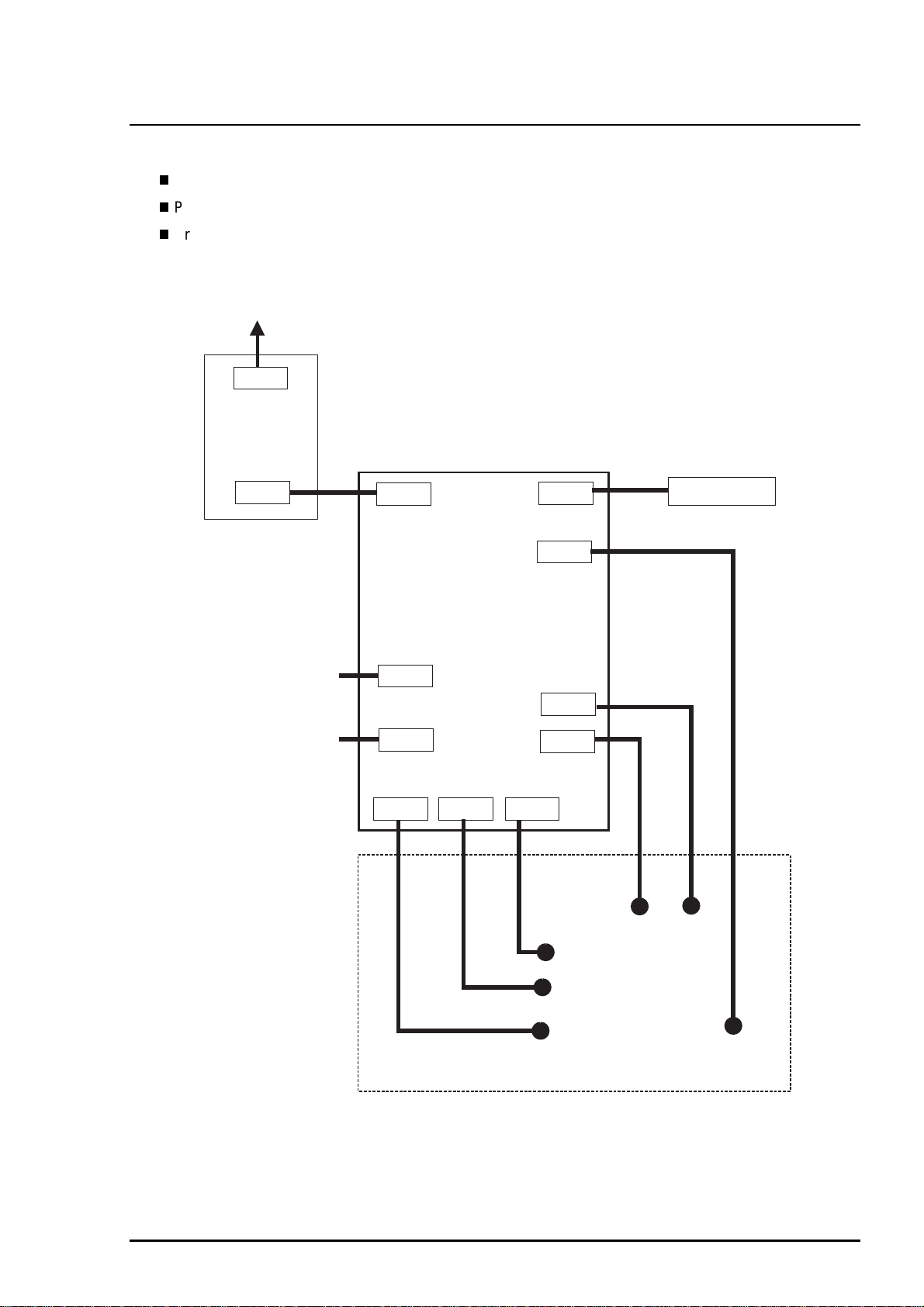
A.1 Connector Summary
Stylus Color 400 has the following primary component units;
Main Board(C206 Main)
Power Supply Board (C206 PSB/PSE)
Printer Mechanism
Figure A-1 below illustrates how these component units are connected.
AC
CN1
C206PSB
(Power Supply
Board)
CN2
Parallel I/F
Serial I/F
CN10
CN1
CN2
CN11
C206 MAIN
(Main Board)
CN5
CN4
CN3
CN8
CN6
CN7
PE Sensor
PF
Motor
Control Panel
CR
Motor
Rev.A
HP Sensor
ASF Sensor
Print Head
Printer Mechanism
Figure A-1. Cable Connection
A-1
Page 3
Appendix
2
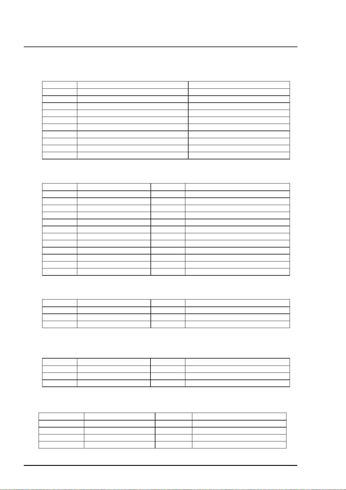
A.2 Connector Summary
Following tables show connector pin assignment of the C206 MAIN board.
Table A-1. Connector summary of the C206 MAIN board
Connector Function Table to refer
CN1 Parallel I/F connector Chapter1/Table 1-10
CN2 Serial I/F connector Chapter1
CN3 •ËControl panel Table A-2
CN4 •ËPE sensor Table A-3
CN5 •ËHP sensor Table A-4
CN6 •ËCR motor Table A-5
CN7 •ËPF motor Table A-6
CN8 •ËPrint head Table A-7
CN10 •ËPower supply board (C206 PSB) Table A-8
CN11 •ËASF sensor Table A-9
Table A-2. Connector CN3
Pin Signal Name I/O Function
1 LED0 Out LED drive signal (0)
2 GND ---- Ground
3 LED1 Out LED drive signal (1)
4 GND ---- Ground
5 LED2 Out LED drive signal (2)
6 +5V ---- Logic power supply
7 +5V ---- Logic power supply
8 LED4 Out LED drive signal (4)
9 SW1 In Panel switch input (1)
10 PSC In Power on/off switch
11 SW0 In Panel switch on/off (0)
12 SW2 In Panel switch on/off (2)
Table A-3. Connector CN4
Pin Signal Name I/O Function
1 PE In Sensor detect signal
2 GND --- Ground
3 PEV --- Sensor power supply(+5V)
Table A-4. Connector CN5
Pin Signal Name I/O Function
1 HP In Sensor detect signal
2 GND --- Ground
3 HPV --- Sensor power supply(+5V)
Table A-5. Connector CN6
Pin Signal Name I/O Function
1 CRA Out Phase drive signal(A)
2 CR-A Out Phase drive signal (-A)
3 CRB Out Phase drive signal (B)
4 CR-B Out Phase drive signal(-B)
A-
Rev. A
Page 4
EPSON Stylus Color400 Service Manual
3
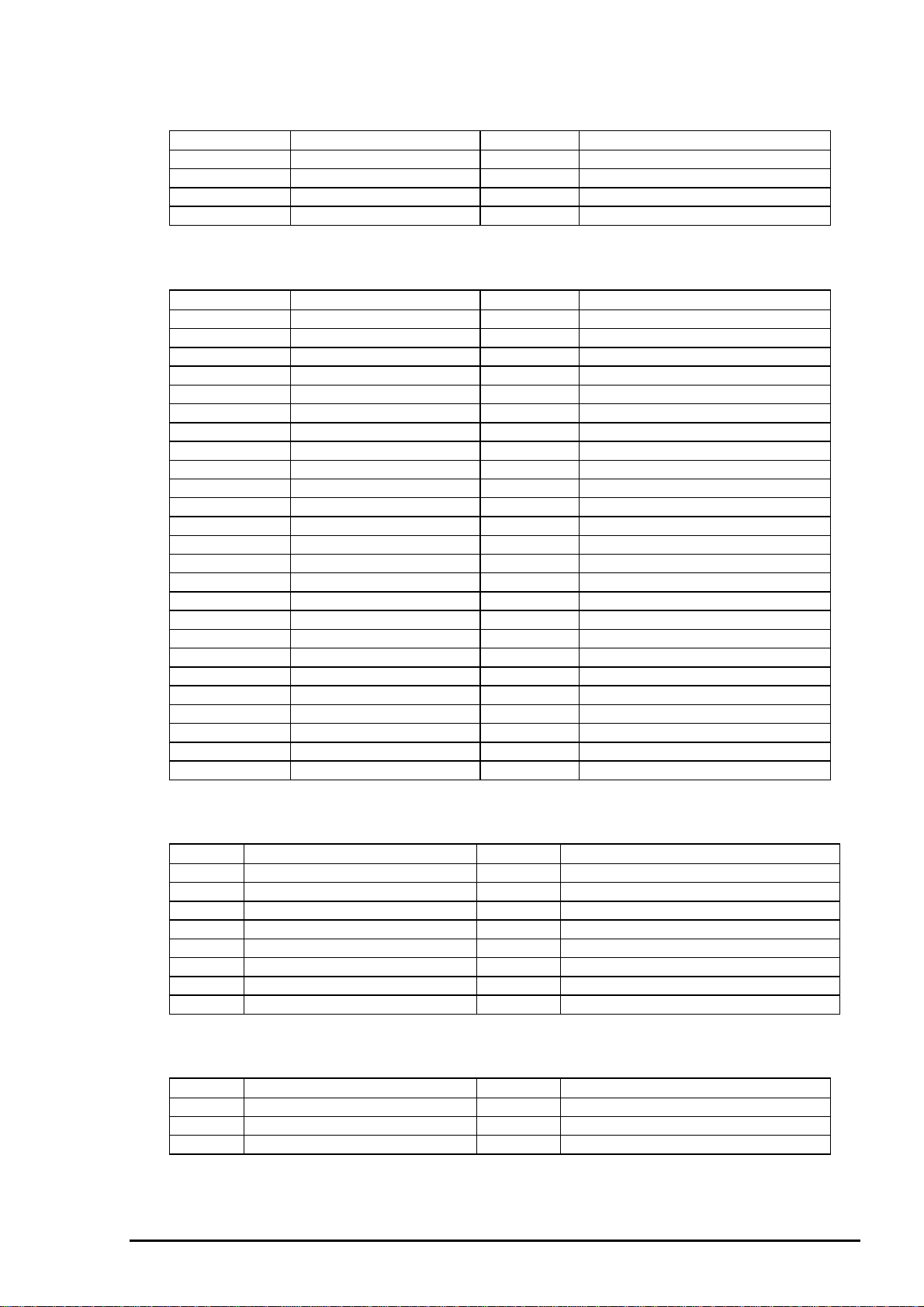
Table A-6. Connector CN7
Pin Signal Name I/O Function
1 PFA Out Phase drive signal (A)
2 PF-A Out Phase drive signal (-A)
3 PFB Out Phase drive signal (B)
4 PF-B Out Phase drive signal(-B)
Table A-7. Connector CN8
Pin Signal Name I/O Function
1 BCO In Black ink cartridge detect signal
2 CCO In Color ink cartridge detect signal
3 THM In Thermistor detect signal
4 GND --- Ground
5 LAT Out Head data latch pulse output
6 GND --- Ground
7 SI3 Out Head data output (3)
8 GND --- Ground
9 SI2 Out Head data output (2)
10 GND --- Ground
11 CLK Out Head data output (1)
12 GND --- Ground
13 CLK Out Clock pulse for head data transfer
14 GND --- Ground
15 NCHG Out Head all on pulse output
16 GND --- Ground
17 VDD --- Logic power supply (+5V)
18 GND2 --- Ground
19 GND2 --- Ground
20 GND2 --- Ground
21 COM --- Head drive power supply
22 COM --- Head drive power supply
23 COM --- Head drive power supply
24 VHV --- Head drive voltage control signal
25 VHV --- Head drive voltage control signal
Rev.A
Table A-8. Connector CN10
Pin Signal Name I/O Function
1 +42V --- Mechanism drive power supply
2 +42V --- Mechanism drive power supply
3 GND --- Ground
4 GND --- Ground
5 PSC Out Power supply switch output signal
6 GND ---- Ground
7 GND --- Ground
8 +5V --- Logic power supply
Table A-9. Connector CN11
Pin Signal Name I/O Function
1 ASF In Sensor detect signal
2 GND --- Ground
3 ASFV --- Sensor power supply (+5V)
A-
Page 5
Appendix
4
A.3 EEPROM Address Map
Address Explanation Setting QPIT
Settings
00H Password 0 54H 01H 0FH 02H Market 0:Word 1:Japan
2:Custom(MJ-)
3:Custom(Stylus Color)
4:Custom (other name)
03H 1st dot adjustment
04H Bi-D adjustment data
05H Uni-D adjustment
-40≤ n ≤40 (by 1/1440 inch)
-36≤ n ≤36 (by 1/1440 inch)
-36≤ n ≤36 (by 1/1440 inch)
∗∗
∗∗
∗∗
00H
00H
00H
00H
06H Reserved 00H 07H Reserved 00H 08H Carriage speed adjustment
-4≤ n ≤4 (by G.A timer unit)
00H
data
09H Reserved 00H 0AH Head actuator rank ID for
12H
VhN
0BH Head actuator rank ID for
01H
Twhs
0CH Reserved 00H 0DH Reserved 00H 0EH Reserved 00H 0FH Reserved 00H -
10H Password 1 5AH 11H 0FH 12H Custom EEPROM sub
00H 00H
number
13H 00H 00H
14H 00H 00H
15H 00H 00H
16H Reserved 00H 17H Reserved 00H 18H CPSI password 00H 00H
19H 00H 00H
1AH 00H 00H
1BH 00H 00H
1CH CPSI flags bit7:CPSI license
00H 00H
0:Disable
1:Enable
bit6:CPSI Font license
0:Disable
1:Enable
1DH Reserved 00H 1EH Reserved 00H 1FH EEPROM Revision 42H -
20H Password 2 5AH 21H 0FH 22H Interface selection 0:Auto 1:Parallel
∗∗
Note)
∗1 Adjusted at factory.
change model name of IEEE1284 device ID.
∗
2 Initialized after performed panel initialization of EEPROM.
2:Serial
00H
Factory
Settings
∗
(
1)
∗
(
1)
∗
(
1)
∗
(
1)
∗
1)
(
∗
(
1)
∗
(
1)
∗
00H
2
A-
Rev. A
Page 6

EPSON Stylus Color400 Service Manual
5
Address Explanation Setting QPIT
settings
settings
23H Interface wait time 0 to 255 (by second) 0AH 0AH
24H Parallel I/F speed 0:High speed 1:Normal 00H 00H
25H Reserved 00H 26H Reserved 00H 27H Print direction control 0:Bi-D 1:Uni-D 2:Auto 02H 02H
28H CG table 0:PC437 1:PC850 00H
29H Reserved 00H -
2AH Auto LF/Network I/F mode bit1:Network I/F mode (0=off, 1=on)
00H 00H
bit0:Auto line feed (0=off, 1=on)
2BH Panel mask function bit5:Extedned settings
00H 00H
bit2:Cleaning
bit1:Replace I/C
bit0:Load/Eject
2CH Reserved 00H 2DH Reserved 00H 2EH Reserved 00H -
2FH Reserved 00H 30H Password 3 5AH 31H 0FH 32H Reserved 00H 33H Reserved 00H 34H Top margin 42 to 44X360 (by 1/360 inch) 78H 78H
35H 00H 00H
36H Reserved 00H 37H Reserved 00H 38H Reserved 00H -
39H Reserved 00H 3AH Reserved 00H 3BH Reserved 00H 3CH Reserved 00H 3DH Reserved 00H 3EH CR-phase of Home 00H 00H
3FH ERROR Number 00H 00H
40H Password 4 5AH -
41H 0FH -
42H Ink flags bit7:resrved
bit6:black
bit5:color
“one time”
“one time”
00H 10H
bit4:Initial fill required
bit3:reserved
bit2:in cleaning seq.
bit1:black CL required
bit0:color CL required
43H Ink flags 2 bit2:YMC cartridge changed and
00H 00H
cleaned
0:first cartridge
1:changed
bit1:Black cartridge changed and
cleaned
0:first cartridge
1:changed
bit0:Black cartridge changed and
cleaned
0:with YMC cartridge
1:alone
Factory
∗
(
1)
Rev.A
A-
Page 7

Appendix
6
Address Explanation Settings QPIT
settings
44H Ink Counter Cb(total)
00H 00H
1count=100(ng)
45H 00H 00H
46H 00H 00H
47H 00H 00H
48H Ink counter CY(total)
00H 00H
1count=100(ng)
49H 00H 00H
4AH 00H 00H
4BH 00H 00H
4CH Ink counter Cy(total)
00H 00H
1count=100(ng)
4DH 00H 00H
4EH 00H 00H
4FH 00H 00H
50H Password 5 5AH 51H 0FH 52H Ink counter Cc(total)
00H 00H
1count=100(ng)
53H 00H 00H
54H 00H 00H
55H 00H 00H
56H Ink counter Csm(total)
00H 00H
1count=100(ng)
57H 00H 00H
58H 00H 00H
59H 00H 00H
5AH Ink counter Csc(total)
00H 00H
1count=100(ng)
5BH 00H 00H
5CH 00H 00H
5DH 00H 00H
5EH Reserved 00H 5FH Reserved 00H -
60H Password 6 5AH 61H 0FH 62H Ink counter Rb 00H 00H
63H 00H 00H
64H Ink counter Ry 00H 00H
65H 00H 00H
66H Ink counter A 00H
67H 00H
68H power off time 00H
69H 00H
6AH CL time 00H
6BH 00H
6CH accumulated printing time 0:0 minute 1:15 minutes 00H 00H
6DH 2:30 minutes 3:60 minutes
00H 00H
4:90 minutes 5:120 minutes
6EH Reserved 00H 6FH Reserved 00H -
70H Password 7 5AH 71H 0FH -
Factory
settigs
∗
00H
2
∗
00H
2
∗
00H
2
∗
00H
2
∗
00H
2
∗
00H
2
A-
Rev. A
Page 8

EPSON Stylus Color400 Service Manual
7
Address Explanation Setting QPIT
settings
72H customized model name string of counter 00H 00H
73H strings of model field for Device 00H 00H
74H ID 00H 00H
75H 00H 00H
76H 00H 00H
77H 00H 00H
78H 00H 00H
79H 00H 00H
7AH 00H 00H
7BH 00H 00H
7CH 00H 00H
7DH 00H 00H
7EH 00H 00H
7FH 00H 00H
settings
Factory
Rev.A
A-
Page 9

Appendix
8
A.4 Circuit Board Component Layouts
Figure A-2. C206 Main Board Component Layout
A-
Rev. A
Page 10

EPSON Stylus Color400 Service Manual
9
Figure A-3. C206 PSB Board Component Layout
Rev.A
A-
Page 11

Appendix
0
Figure A-4. C206 PSE Board Component Layout
A-1
Rev. A
Page 12

EPSON Stylus Color400 Service Manual
Figure A-5. C206 PNL Component Layout
Rev.A
A-11
Page 13

Appendix
2
A.5 Exploded Diagrams
Figure A-6.Stylus Color 400 Exploded Diagram (1)
A-1
Rev. A
Page 14

EPSON Stylus Color400 Service Manual
3
Figure A-7. Stylus Color 400 Exploded Diagram (2)
Rev.A
A-1
Page 15

Appendix
4
Figure A-8. Stylus Color 400 Exploded Diagram (3)
A-1
Rev. A
 Loading...