

Page 1

PF282-07
SED1278F/D
SED1278F/D
Dot Matrix LCD Controller Driver
1/8, 1/11 or 1/16 Duty Dot Matrix Drive
Built-in Character Generator ROM and RAM ( )
Maximum Simultaneous Display of 80 Characters
(With extension LCD driver)
DESCRIPTION
The SED1278F/D is a dot matrix LCD controller/driver which is dedicated to character display. It is capable of
displaying up to 80 characters under 4-bit/8-bit MPU control.
The built-in character generator ROM has an extended capacity of 240 different characters, each being generated
in a 5 10 dots font compatible with a 1/11 duty. In addition, the SED1278F/D contains 64 bytes of character
generator RAM in which the user can store 8 different characters, each consisting of 5 8 dots. These memory
features offer high flexibility in character display.
The guaranteed minimum LCD driving voltage is 3V, and this makes the SED1278F/D suitable for driving low
voltage LCDs.
FEATURES
Display RAM............................... 80 bytes (80 characters)
Character generator ROM.......... 240 characters (Able to 256 characters)
Character generator RAM .......... 8 characters
Built-in CR oscillator, Built-in power-on reset circuit
Maximim display dimension ....... 40 characters 2 lines, 80 characters 1 line
(When accompanied with SED1181FLA/DLA, SED1681FOA/DOA)
1/8, 1/11 or 1/16 duty matirx drive (fixed by command)
2 flame AC wave-form drive
High-speed bus interface with 4-bit/8-bit MPU
Powerful display control instructions
Character.................................... 5 7 dots+Cursor line (5 8 dots also possible)
5 10 dots+Cursor line
6 Kinds of character font
Single power supply ................... 5V±10% (Logic)
Low LCD driving voltage ............ VDD-V
Package ..................................... SED1278F: QFP5-80pin (plastic)
SED1278D: Die form (Al pad)
5
>
=
3.0V
ROM 240 characters
RAM 8 characters
BLOCK DIAGRAM
DB0
DB7
E
R
RS
V
V
V1
V2
V3
V4
V5
OSC1 OSC2
Address
Counter ACC
7
Cursor/
Brink Control
Display Data RAM
5 10 240 Byts
55
MPX
5
Parallel/Serial
Data Converter
Refresh Address Counter
7
MPX
DD RAM
80 Bytes
8
Character
Generator
RAM
(CG RAM)
Oscillation
Circuit
Timing Generator
Shift Register 16 Bits
Common Driving
Output Circuit
Segment Driving
Output Circuit
Latch Circuit
40 Bits
Shift Register
40 Bits
XSCL
LP
FR
COM1
~~
COM16
SEG1
SEG40
D0
1
Instruction Decoder
Instruction Register
~
I/O BufferI/O Control
/
W
DD
SS
8
Data Register
8
MPX
Character
Generator
8
RAM
(CG RAM)
64 Bytes
SEIKO EPSON CORPORATION
Page 2

SED1278F/D
PIN CONFIGURATION
QFP5-80pin
SEG39
SEG40
COM16
COM15
COM14
COM13
COM12
COM11
COM10
COM9
COM8
COM7
COM6
COM5
COM4
COM3
COM2
COM1
DB7
DB6
DB5
DB4
DB3
DB2
PIN DESCRIPTION
Symbol
RS
R/W
E
DB0 to DB7
LP
XSCL
FR
DO
COM 1 to COM16
SEG1 to SEG40
V1 to V5
V
DD
V
SS
OSC1
OSC2
SEG38
SEG37
SEG36
SEG35
SEG34
SEG33
SEG32
SEG31
SEG30
SEG29
SEG28
SEG27
SEG26
SEG25
SEG24
SEG23
No. of signals
1
1
1
8
1
1
1
1
16
40
5
1
1
2
DB1
404550556065
DB0
E
R/W
70
SED1278F
INDEX
75
80
510152025
1
SEG22
SEG21
SEG20
SEG19
SEG18
SEG17
SEG16
SEG15
SEG14
SEG13
SEG12
SEG11
SEG10
SEG9
SEG8
SEG7
SEG6
SEG5
SEG4
SEG3
SEG2
SEG1
RS
D0
35
FR
DD
V
XSCL
LP
V5
30
V4
V3
V2
V1
OSC2
SS
V
OSC1
Function
Register select signal
Read/write select signal
Read/write execute signal
Data bus
Data latching pulse
Data transfer clock
LCD AC driving signal
Serial data
Common outputs
COM9 to COM16: non-select for 1/8 duty
COM12 to COM16: non-select for 1/11 duty
Segment outputs
LCD driving power (V
>
VSS)
=
5
+5V
0V (GND)
Used to connect resistor (typ. 91K-ohms) for oscillation;
OSC1 is for external clock input.
Unit: mm
1
1
RS
R/W E Operation
0
0
1
1
ABSOLUTE MAXIMUM RATINGS
Rating
Supply voltage (1)
Supply voltage (2)
Input voltage
Output voltage
Power dissipation
Operating temperature
Storage temperature
Soldering temperature and time
Note: The following condition must always hold true: V
2
Symbol
V
V1 to V
V
P
T
T
T
0
11
0
DD
1
>
>
V
V
1
=
=
1
V
DD
5
I
O
D
opr
stg
sol
Instruction write cycle
Busy flag read cycle
Address counter read cycle
DD RAM or CG RAM data write cycle
DD RAM or CG RAM data read cycle
260˚C 10s (at lead)
>
>
V
V
2
3
=
=
Value
-0.3 to 7.0
-0.3 to V
-0.3 to V
-0.3 to V
-20 to 75
-65 to 150
>
V
4
5
=
300
DD
DD
DD
+0.3
+0.3
+0.3
(VSS=0V, Ta=25˚C)
Unit
V
V
V
V
mW
˚C
˚C
—
Page 3
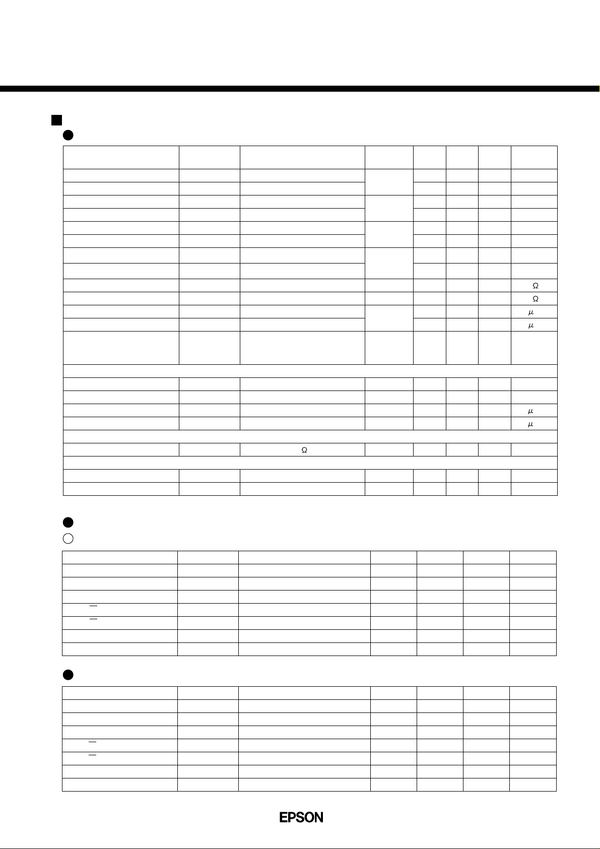
ELECTRICAL CHARACTERISTICS
DC Characteristics
Characteristic
"H" level input voltage (1)
"L" level input voltage (1)
"H" level input voltage (2)
"L" level input voltage (2)
"H" level output voltage (1)
"L" level output voltage (1)
"H" level output voltage (2)
"L" level output voltage (2)
Driver-on resistor (COM)
Driver-on resistor (SEG)
I/O leakage current
Pull-up MOS current
Symbol
V
IH1
V
IL1
V
IH2
V
IL2
V
OH1
V
OL1
V
OH2
V
OL2
R
COM
R
SEG
I
IL
-I
P
Rf oscillation, from
Supply current
I
OP
external clock
V
External clock operation
External clock operating frequency
External clock duty
External clock rise time
External clock fall time
f
EXTCL
Duty
tr
EXTCL
tf
EXTCL
Internal clock operation (Rf oscillation)
Oscillation frequency
f
OSC
Internal clock operation (Ceramic filter oscillation)
Oscillation frequency
LCD driving voltage
V
f
OSC
LCD
Condition
I
=-0.205mA
OH
I
=1.6mA
OL
I
=-0.04mA
OH
=0.04mA
I
OL
COM-Vn
SEG-Vn
V
=0 to V
I
|=0.5V
|=0.5V
DD
|V
|V
VDD=5V
=5V, fosc=fCP=270kHz
DD
R
=91K ±2%
f
Ceramic filter
V
DD-V5
Applicable
Pin
DB0~DB7
RS, R/W, E
OSC1
DB0~DB7
XSCL
LP
DO
COM1~16
SEG1~40
V
DD
SED1278F/D
=5.0V±10%, VSS=0V, Ta=-20 to 75˚C)
(V
DD
Min.
2.0
V
VDD-1.0
V
2.4
0.9V
125
190
245
3.0
—
—
—
—
—
50
—
45
SS
SS
-
-
DD
Typ.
—
—
—
—
—
—
—
—
2
2.5
—
125
0.5
250
50
—
—
270
250
—
Max.
V
0.8
V
1.0
0.4
0.1V
10
10
250
0.8
350
55
0.2
0.2
350
255
V
DD
DD
—
—
DD
1
DD
Unit
V
V
V
V
V
V
V
V
k
k
A
A
mA
kHz
%
S
S
kHz
kHz
V
AC Characteristics
Read Cycle
Characteristic
Enable cycle time
Enable "H" level pulse width
Enable rise/fall time
RS, R/W setup time
RS, R/W address hold time
Read data output delay
Read data hold time
Write Cycle
Characteristic
Enable cycle time
Enable "H" level pulse width
Enable rise/fall time
RS, R/W setup time
RS, R/W address hold time
Data setup time
Write data hold time
Symbol
t
cycE
t
WEH
trE, t
fE
t
AS
t
AH
t
RD
t
DHR
Symbol
t
cycE
t
WEH
trE, t
fE
t
AS
t
AH
t
DS
t
DH
Condition
CL=100pF
(VDD=5.0V±10%, VSS=0V, Ta=-20 to 75˚C)
Min.
500
220
—
40
10
—
20
Typ.
—
—
—
—
—
—
—
Max.
—
—
25
—
—
120
—
(VDD=5.0V±10%, VSS=0V, Ta=-20 to 75˚C)
Min.
500
220
—
40
10
60
10
Typ.
—
—
—
—
—
—
—
Max.
—
—
25
—
—
—
—
Unit
ns
ns
ns
ns
ns
ns
ns
UnitCondition
ns
ns
ns
ns
ns
ns
ns
3
Page 4
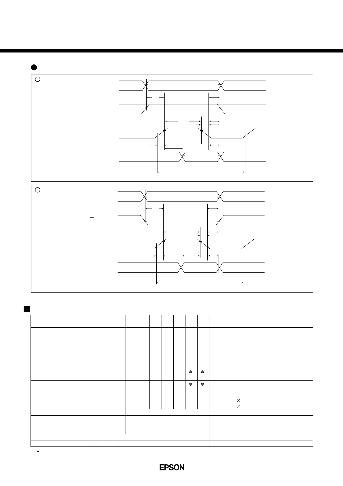
SED1278F/D
Read Cycle
RS
V
IH1
V
IH1
V
IH1
V
IH1
V
IH1
V
IL1
V
OH1
V
OL1
V
OH1
Significant
Data
V
OL1
V
IL1
V
IL1
V
IL1
V
IH1
V
IL1
R/W
E
DB0 to DB7
t
AS
t
cycE
t
RD
t
WEH
t
AH
t
AH
t
fE
t
fE
t
DHR
RS
V
IH1
V
IL1
V
IH1
V
IH1
V
IL1
V
IL1
V
IH1
V
IL1
V
IH1
Significant
Data
V
IL1
V
IL1
V
IL1
V
IL1
V
IH1
V
IL1
E
DB0 to DB7
t
AS
t
cycE
t
WEH
t
DS
t
AH
t
AH
t
fE
t
fE
t
DH
Write Cycle
R/W
Timing Chart
DISPLAY COMMAND
CLEAR DISPLAY
CURSOR HOME
ENTRY MODE SET
DISPLAY ON/OFF
CURSOR/DISPLAY SHIFT
SYSTEM SET
SET CGRAM ADDRESS
SET DDRAM ADDRESS
READ BUSY FLUG/
WRITE DATA
READ DATA
4
Parameter NoteRS R/W DB7 DB6 DB5 DB4 DB3 DB2 DB1 DB0
0
0
0
0
0
0
0
0
0
0
0
0
0
0
BF
0
0
0
0
0
0
0
0
0
0
1
1
0
0
0
0
0
0
0
1
0
0
0
0
0
1
0
0
0
1
DL
AC
ADDRESS COUNTER
Don‘t care
0
1
1
1
Write Data
Read Data
0
0
0
0
0
1
1
D
S/C
R/L
N
F
A
CG
A
DD
I/D
C
0
1
1
1
I/D
DB1=1: Increment, DB1=0: Decrement
DB0=1: The display is shifted.
DB0=0: The display is not shifted.
C
DB2=1: Display on DB2=0: Display off
DB1=1: Cursor on DB1=0: Cursor off
DB0=1: Brinking on DB0=0: Brinking off
DB3=1: Shifts display one character
DB2=1: Right shift, DB2=0: Left shift
DB4=1: 8 bits, DB4=0: 4 bits
DB3=1: 2 lines display (1/16 duty),
DB3=0: 1 line display
DB2=1: 5 10 dots, 1/11 duty
( )
DB2=0: 5 7 dots, 1/8 duty
The address length that can be set is 64 addresses.
The address length that can be set is 80 addresses.
DB7=1: Busy (instruction not accepted)
DB7=0: Ready (instruction accepted)
Page 5

20
±0.1
25.6
±0.4
4164
14
±0.1
19.6
±0.4
25
40
INDEX
0.35
±0.1
241
80
65
2.7
±0.1
0.26
3.4
max
2.8
1.5
0°
12°
0.15
±0.05
0.8
Plastic QFP5-80pin
Unit: mm
PACKAGE DIMENSIONS
LCD PANEL INTERFACE EXAMPLE (2 lines 20 characters)
SED1278F/D
SED1278F/D is usually connected to 8-bit MPU via I/O ports.
SED1278F/D
COM1
…
COM16
SEG1
…
SEG40
DO
LP
XSCL
FR
V
DD
V
SS
V2
V3
V5
OSC1 OSC2
R
f
LCD
16
40 60
16 100 dots
DO DO1
…
SEG0
SED1181F/D
LP
SEG59
LA
XSCLFRVDDVSSV2V3V
D1
DO0
OPEN
SSH
5
Page 6

SED1278F/D
1
2
3
4
5
6
7
8
9
10
11
12
13
14
15
16
17
18
19
20
21
22
23
24
25
26
27
SEG22
SEG21
SEG20
SEG19
SEG18
SEG17
SEG16
SEG15
SEG14
SEG13
SEG12
SEG11
SEG10
SEG9
SEG8
SEG7
SEG6
SEG5
SEG4
SEG3
SEG2
SEG1
GND
OSC1
OSC2
V
1
V
2
2,087
1,905
1,723
1,541
1,359
1,177
995
814
633
452
272
91
-91
-272
-452
-633
-814
-995
-1,177
-1,359
-1,541
-1,723
-1,905
-2,087
1,671
1,365
1,183
1,001
Pad No. Pad Name X Y
Unit: m
55
56
57
58
59
60
61
62
63
64
65
66
67
68
69
70
71
72
73
74
75
76
77
78
79
80
COM9
COM10
COM11
COM12
COM13
COM14
COM15
COM16
SEG40
SEG39
SEG38
SEG37
SEG36
SEG35
SEG34
SEG33
SEG32
SEG31
SEG30
SEG29
SEG28
SEG27
SEG26
SEG25
SEG24
SEG23
452
633
814
995
1,177
1,359
1,541
1,723
1,905
2,087
-1,671
-1,365
-1,183
-1,001
-819
-637
-455
-273
-91
91
273
455
637
819
1,001
1,183
1,365
Pad No. Pad Name X Y
28
29
30
31
32
33
34
35
36
37
38
39
40
41
42
43
44
45
46
47
48
49
50
51
52
53
54
V
3
V
4
V
5
LP
XSCL
V
CC
FR
DO
RS
R/W
E
DB0
DB1
DB2
DB3
DB4
DB5
DB6
DB7
COM1
COM2
COM3
COM4
COM5
COM6
COM7
COM8
-2,087
-1,905
-1,723
-1,541
-1,359
-1,177
-995
-814
-633
-452
-272
-91
91
272
819
637
455
273
91
-91
-273
-455
-637
-819
-1,001
-1,183
-1,365
-1,671
Pad No. Pad Name X Y
SED1278D
PAD LAYOUT
Unit: m
PAD COORDINATION
6
24
25
40
41
4,500
Y
(0, 0)
1
80
X
64
3,670
Monitor Pad
65
Pad size: 109 109
Page 7

SED1278DOA CHARACTER FONT
SED1278F/D
7
Page 8

SED1278F/D
SED1278F
OB/DOB
CHARACTER FONT
8
Page 9

SED1278F
OC/DOC
SED1278F/D
CHARACTER FONT
9
Page 10

SED1278F/D
SED1278FOD/
DOE CHARACTER FONT
10
Page 11

SED1278F
OG/DOG
SED1278F/D
CHARACTER FONT
11
Page 12

SED1278F/D
SED1278F
OH/DOH
CHARACTER FONT
12
Page 13

SED1278F/D
NOTICE
No part of this material may be reproduced or duplicated in any form or by any means without the written permission of Seiko
Epson. Seiko Epson reserves the right to make changes to this material without notice. Seiko Epson does not assume any liability
of any kind arising out of any inaccuracies contained in this material or due to its application or use in any product or circuit and,
further, there is no representation that this material is applicable to products requiring high level reliability, such as, medical
products. Moreover, no license to any intellectual property rights is granted by implication or otherwise, and there is no
representation or warranty that anything made in accordance with this material will be free from any patent or copyright
infringement of a third party. This material or portions thereof may contain technology or the subject relating to strategic products
under the control of the Foreign Exchange and Foreign Trade Control Law of Japan and may require an export license from the
Ministry of International Trade and Industry or other approval from another government agency.
All product names mentioned herein are trademarks and/or registered trademarks of their respective companies.
©Seiko Epson Corporation 1999 All rights reserved.
ELECTRONIC DEVICES MARKETING DIVISION
IC Marketing & Engineering Group
ED International Marketing Department I (Europe & U.S.A.)
421-8, Hino, Hino-shi, Tokyo 191-8501, JAPAN
Phone: +81-(0)42-587-5812 Fax: +81-(0)42-587-5564
ED International Marketing Department II (Asia)
421-8, Hino, Hino-shi, Tokyo 191-8501, JAPAN
Phone: +81-(0)42-587-5814 Fax: +81-(0)42-587-5110
13
 Loading...