

Page 1

Power Supply IC
S1F77B01
Technical Manual
SEIKO EPSON CORPORATION
Rev.1.3
Page 2

NOTICE
No part of this material may be reproduced or duplicated in any form or by any means without the written
permission of Seiko Epson. Seiko Epson reserves the right to make changes to this material without notice.
Seiko Epson does not assume any liability of any kind arising out of any inaccuracies contained in this material
or due to its application or use in any product or circuit and, further, there is no representation that this material is
applicable to products requiring high level reliability, such as, medical products. Moreover, no license to any
intellectual property rights is granted by implication or otherwise, and there is no representation or warranty that
anything made in accordance with this material will be free from any patent or copyright infringement of a third
party. This material or portions thereof may contain technology or the subject relating to strategic products
under the control of the Foreign Exchange and Foreign Trade Law of Japan and may require an export license
from the Ministry of International Trade and Industry or other approval from another government agency.
All other product names mentioned herein are trademarks and/or registered trademarks of their respective
companies.
©SEIKO EPSON CORPORATION 2006, All rights reserved.
Page 3

Configuration of product number
zDEVICES
S1 F 77B01 B 0C00 00
Packing specifications
Specifications
Shape
(B:WCSP, Y:SOT)
Model number
Model name
(F : Power Supply)
Product classification
(S1:Semiconductors)
Page 4

CONTENTS
1. DESCRIPTION.................................................................................................................................1
2. FEATURES ......................................................................................................................................1
3. PACKAGE........................................................................................................................................1
4. APPLICATION .................................................................................................................................1
5. BLOCK DIAGRAM...........................................................................................................................2
6. SELECTION GUIDE.........................................................................................................................3
7. PIN ASSIGNMENT...........................................................................................................................3
8. MARKING ........................................................................................................................................4
9. MARKING ........................................................................................................................................5
10. PIN DESCRIPTION..........................................................................................................................6
11. ABSOLUTE MAXIMUM RATINGS ..................................................................................................6
12. TIMING CHARTS AND RECOMMENDED CIRCUIT DIAGRAMS...................................................7
13. ELECTRICAL CHARACTERISTICS, DELAY CIRCUIT BUILT-IN PRODUCTS..............................8
14. CHARACTERISTIC MEASURING CIRCUITS.................................................................................9
15. DIMENSIONS.................................................................................................................................12
16. CHARACTERISTIC EXAMPLE .....................................................................................................14
S1F77B01 Technical Manual (Rev.1.3) EPSON i
Page 5

1. DESCRIPTION
1. DESCRIPTION
The S1F77B01 is a CMOS detector that runs at superlow consumption current 350nA (Typ.).
The detecting voltage can be selected in the range from 1.5V to 4.6V which is set to high accuracy ±2.0% in
0.1V steps. The power voltage is allowable in the range of low voltage 0.9 to 5.5V.
This detector adopts a compact package, which is available in a compact mobile device.
2. FEATURES
• Superlow power consumption: 350nA (VDD=3.0V, Typ.)
• Range of detecting voltage: 1.5 to 4.6V (in 0.1V steps)
• Accuracy of detecting voltage: ±2.0%
• Hysteresis characteristics: 5.0% Typ.
• Temperature characteristics of detecting voltage: ±100 ppm/°C (Typ.)
• Output type: CMOS, Nch open drain
3. PACKAGE
SOT23 5pin
WCSP 4pin
4. APPLICATION
• Microcomputer and logic circuit resetting
• Battery checker
• Level discriminator
• Waveform rectifier circuit
• Backup power switching circuit
• Power failure detector
• Overcurrent protection circuit
S1F77B01 Technical Manual (Rev.1.3) EPSON 1
Page 6
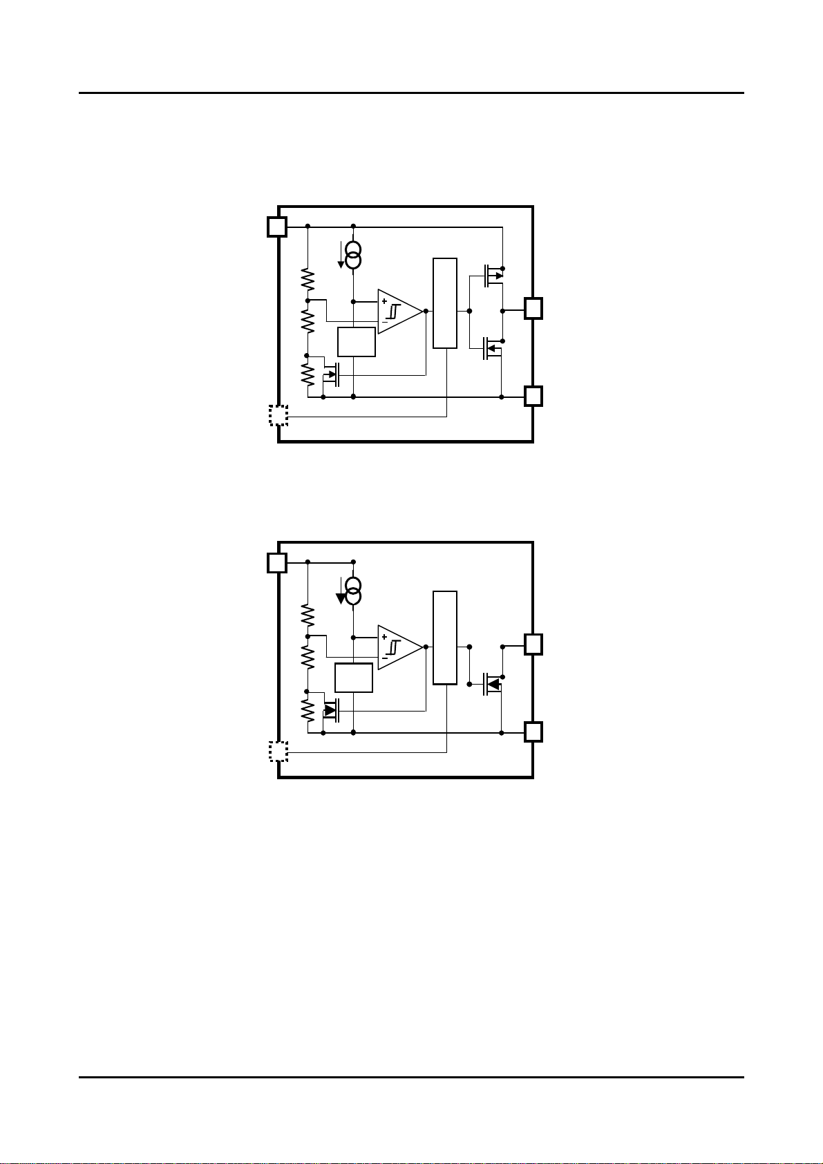
5. BLOCK DIAGRAM
5. BLOCK DIAGRAM
zCMOS output
zNch open drain output
Note: SOT23 package product only; otherwise, a product with DS pin set to NC
The DS pin must be fixed to “LOW” outside the IC.
V
DD
DS*
DD
V
DS*
VREF
Delay circuit
VREF
Delay circuit
V
V
V
V
OUT
SS
OUT
SS
2 EPSON S1F77B01 Technical Manual (Rev.1.3)
Page 7

6. SELECTION GUIDE
S1F77B01 *
a b c d e
a Package type
b Indicates a value that is ten times the detecting voltage.
c For CMOS output, delay 50ms “C”
For CMOS output, delay 100ms “D”
For CMOS output, delay 200ms “E”
For Nch open drain output, delay 50ms “L”
For Nch open drain output, delay 100ms “M”
For Nch open drain output, delay 200ms “N”
d Fixed to 0 in this IC.
e Taping form
7. PIN ASSIGNMENT
SOT23 5PIN
DD
V
5
1 3
DS
2
SS
V
* * * 0 * *
SOT23 5PIN “Y”
WCSP 4PIN “B”
TR type “0R”
VOUT
4
NC
WCSP 4PIN
Top View
6. SELECTION GUIDE
V
DD
DS
VOUT
3
4
1 2
VSS
S1F77B01 Technical Manual (Rev.1.3) EPSON 3
Page 8

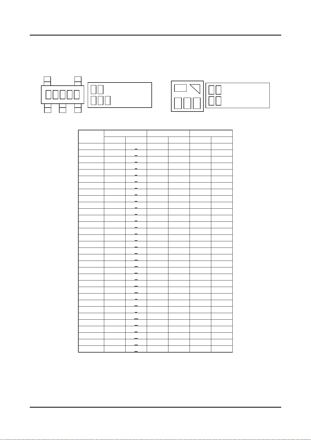
8. MARKING
8. MARKING
SOT23 5PIN WCSP 4PIN
5
a b c
1 2
d e
4
a
b
: Product code
e
c
3
CMOS
Vdet-
Option
1.5V B 5 B 5 B _5
1.6V B 6 B 6 B _6
1.7V B 7 B 7 B _7
1.8V B 8 B 8 B _8
1.9V B 9 B 9 B _9
2.0V J 0 J 0 J _0
2.1V J 1 J 1 J _1
2.2V J 2 J 2 J _2
2.3V J 3 J 3 J _3
2.4V J 4 J 4 J _4
2.5V J 5 J 5 J _5
2.6V J 6 J 6 J _6
2.7V J 7 J 7 J _7
2.8V J 8 J 8 J _8
2.9V J 9 J 9 J _9
3.0V J A J A J _A
3.1V J B J B J _B
3.2V J C J C J _C
3.3V J D J D J _D
3.4V J E J E J _E
3.5V J F J F J _F
3.6V J G J G J _G
3.7V J H J H J _H
3.8V J J J J J _J
3.9V J K J K J _K
4.0V J L J L J _L
4.1V J M J M J _M
4.2V J N J N J _N
4.3V J P J P J _P
4.4V J Q J Q J _Q
4.5V J R J R J _R
4.6V J S J S J _S
: Lot code
d
Delay time 50ms Delay time 100ms Delay time 200ms
a b a b a b
34
d
b
a
c
1
2
Top View
a
: Product code
b
: Lot code
c d
4 EPSON S1F77B01 Technical Manual (Rev.1.3)
Page 9
9. MARKING
SOT23 5PIN WCSP 4PIN
5
a
b c d e
1 2
4
a
b
: Product code
c
e
: Lot code
d
3
Nch open drain
Vdet-
Option
1.5V B 5 B 5 B _5
1.6V B 6 B 6 B _6
1.7V B 7 B 7 B _7
1.8V B 8 B 8 B _8
1.9V B 9 B 9 B _9
2.0V J 0 J 0 J _0
2.1V J 1 J 1 J _1
2.2V J 2 J 2 J _2
2.3V J 3 J 3 J _3
2.4V J 4 J 4 J _4
2.5V J 5 J 5 J _5
2.6V J 6 J 6 J _6
2.7V J 7 J 7 J _7
2.8V J 8 J 8 J _8
2.9V J 9 J 9 J _9
3.0V J A J A J _A
3.1V J B J B J _B
3.2V J C J C J _C
3.3V J D J D J _D
3.4V J E J E J _E
3.5V J F J F J _F
3.6V J G J G J _G
3.7V J H J H J _H
3.8V J J J J J _J
3.9V J K J K J _K
4.0V J L J L J _L
4.1V J M J M J _M
4.2V J N J N J _N
4.3V J P J P J _P
4.4V J Q J Q J _Q
4.5V J R J R J _R
4.6V J S J S J _S
Delay time 50ms Delay time 100ms Delay time 200ms
a b a b a b
34
d
abc
2
1
Top View
a
: Product code
b
: Lot code
c d
9. MARKING
S1F77B01 Technical Manual (Rev.1.3) EPSON 5
Page 10

10. PIN DESCRIPTION
10. PIN DESCRIPTION
For SOT-23-5
Pin No. Pin Name Function
1 DS Fixed to “LOW”.
2 VSS GND pin.
3 NC No connection
4 VOUT Voltage detection output pin
5 VDD Power input pin
For WCSP
Pin No. Pin Name Function
1 DS Fixed to “LOW”.
2 VSS GND pin.
3 VDD Voltage output pin
4 VOUT Power detection output pin
11. ABSOLUTE MAXIMUM RATINGS
a=25°C RL=∞ unless otherwise specified)
(T
Item Symbol Rating Unit
Power voltage VDD-VSS 7.0 V
Output voltage
Output current IOUT 20 mA
Allowable dissipation PD
Guaranteed operating temperature range Topr -40 to +85 °C
Storage temperature range Tstg -40 to +125 °C
Note: To stabilize the IC, insert the decoupling capacitor between V
Nch open drain output VSS-0.3V to 7.0
CMOS output
VOUT
SOT23 300 mW
WCSP 100 mW
VSS-0.3V to VDD+0.3V
DD and VSS.
V
6 EPSON S1F77B01 Technical Manual (Rev.1.3)
Page 11

12. TIMING CHARTS AND RECOMMENDED CIRCUIT DIAGRAMS
12. TIMING CHARTS AND RECOMMENDED CIRCUIT DIAGRAMS
zCMOS
Power
voltage
V
DD
Output
voltage
zNch open drain
Power
voltage
V
DD
Output
voltage
Release voltage
V
DET+
Detecting voltage
DET-
V
Min. operating
voltage
V
SS
Release voltage
V
DET+
Detecting voltage
DET-
V
Min. operating
voltage
VSS
Hysteresis width
Hysteresis width
td
td
VDD
V
V
SS
VDD
VSS
V
OUT
OUT
DS
Recommended circuit diagram
DS
Recommended circuit diagram
V
R
470kΩ
V
S1F77B01 Technical Manual (Rev.1.3) EPSON 7
Page 12

13. ELECTRICAL CHARACTERISTICS, DELAY CIRCUIT BUILT-IN PRODUCTS
13. ELECTRICAL CHARACTERISTICS, DELA Y CIRCUIT BUILT -IN PRODUCTS
(1) CMOS output
a=25°C RL=∞ unless otherwise specified)
(T
Item Symbol Conditions Min. Typ. Max. Unit
Detecting voltage VDET-
Hysteresis width VHYS VHYS=(VDET+)-(VDET-) VDET-*0.03 VDET-*0.05 VDET-*0.07 V
VDD=2.5V, VDET-(S)=1.5V
Consumption current 1 ISS1
Consumption current 2 ISS2
Max. operating voltage VDDH
Min. operating voltage VDDL
IOUTN
Output current
I
OUTP
Delay time td
Response time tPHL VDD: (VDET-(S))+1.0V ===> 0.9V
Detecting voltage
temperature
coefficient
∆V
∆Topt
DET
VDD=3.7V, VDET-(S)=2.7V
DD=5.5V, VDET-(S)=4.6V
V
VDD=1.3V, VDET-(S)=1.5V
VDD=2.5V, VDET-(S)=2.7V
DD=4.4V, VDET-(S)=4.6V
V
[Nch]
DD<VDET-
V
[Pch]
DD>VDET-
V
-40°C≦Topt≦85°C
(2) Nch open drain output
Item Symbol Conditions Min. Typ. Max. Unit
Detecting voltage VDET-
Hysteresis width VHYS VHYS=(VDET+)-(VDET-) VDET-*0.03 VDET-*0.05 VDET-*0.07 V
VDD=2.5V, VDET-(S)=1.5V
Consumption current 1 ISS1
Consumption current 2 ISS2
Max. operating voltage VDDH
Min. operating voltage VDDL
Output current of
output transistor
Leak current of output
transistor
Delay time td
Response time tPHL VDD: (VDET-(S))+1.0V ===> 0.9V
Detecting voltage
temperature
coefficient
IOUTN
ILEAK VDD=5.5V,VDS=5.5V
DET
∆V
∆Topt
VDD=3.7V, VDET-(S)=2.7V
DD=5.5V, VDET-(S)=4.6V
V
VDD=1.3V, VDET-(S)=1.5V
VDD=2.5V, VDET-(S)=2.7V
DD=4.4V, VDET-(S)=4.6V
V
[Nch]
VDD<VDET-
-40°C≦Topt≦85°C
-
VDET-(S)×0.98 VDET-(S) VDET-(S)×1.02 V
-
-
350 700
-
350 700
-
280 560
-
280 560
-
280 560
-
-
0.9
VDD=0.9V, VDS=0.5V 0.2 0.8 1.5
VDD=1.2V, VDS=0.5V 1.0 2.2 3.5
DD=2.4V, VDS=0.5V 5.5 6.8 8.1
V
VDD=3.0V,
DS=VDD-0.5V
V
VDD=4.0V,
DS=VDD-0.5V
V
DD=5.5V,
V
VDS=VDD-0.5V
-
2.5 4.5 7.0
4.5 6.2 8.0
6.5 8.2 9.8
350 700
nA
nA
-
5.5 V
-
-
V
mA
td=50ms 42.5 50 57.5
td=100ms 85 100 115
ms
td=200ms 170 200 230
-
-
±100
a=25°C RL=∞ unless otherwise specified)
(T
-
VDET-(S)×0.98 VDET-(S) VDET-(S)×1.02 V
-
-
350 700
-
350 700
-
280 560
-
280 560
-
280 560
-
-
0.9
VDD=0.9V, VDS=0.5V 0.2 0.8 1.5
VDD=1.2V, VDS=0.5V 1.0 2.2 3.5
DD=2.4V, VDS=0.5V 5.5 6.8 8.1
V
-
-
-
80 µs
-
ppm/°C
350 700
nA
nA
-
5.5 V
-
-
0.1 µA
-
V
mA
td=50ms 42.5 50 57.5
td=100ms 85 100 115
ms
td=200ms 170 200 230
-
-
±100
-
80 µs
-
ppm/°C
8 EPSON S1F77B01 Technical Manual (Rev.1.3)
Page 13

14. CHARACTERISTIC MEASURING CIRCUITS
AB A
14. CHARACTERISTIC MEASURING CIRCUITS
DET-, VHYS, tPLH, td
V
VDD
SS1, ISS2
I
V
VDD
VDD VOUT
VSS
DS
A
Fig.1
Fig.2
V
5V
470kΩ
V
Note: No pull-up resistor for
: When fixed to DS=”LOW”
B: When fixed to DS=”HIGH”
DD
VSS, DS
CMOS output
OUT
V
S1F77B01 Technical Manual (Rev.1.3) EPSON 9
Page 14

14. CHARACTERISTIC MEASURING CIRCUITS
IOUT Nch, ILEAK
OUT Pch
I
DD
V
V
VDD
VSS, DS
Fig.3
VOUT
VSS, DS
Fig.4
A
VV
V
A
10 EPSON S1F77B01 Technical Manual (Rev.1.3)
Page 15

zDescription of tPHL
Input: VDD
VDD=VDET+ +1.0V
*3
VDD=0.9V
VOUT
Output:
VDD=VDET+ +1.0V
VOUT=VDD(0.9V)
SS
V
DET+ indicates the actual release voltage. VDET+=VDET-×1.05 (Typ.)
*3: V
(1) For CMOS output
tPHL provides the timeframe ranging from a time when the pulse voltage (VDET+)+1.0V → 0.9V is
applied to V
(2) Nch open drain output
DD, to a time when the output voltage reaches VDD/2.
tPHL provides the timeframe ranging from a time when the pulse voltage (VDET+)+1.0V → 0.9V is
applied to V
The output pin is pulled up with 470kΩ resistance and V
zDescription of
Input: V
DD
Output:
VOUT
(1) For CMOS output
DD, to a time when the output voltage reaches VDD/2.
td
VDD=VDET+ +1.0V
DD=0.9V
V
VOUT= 100 %
V
SS
td provides the timeframe ranging from a time when the pulse voltage 0.9V → (VDET+)+1.0V is
applied to V
(2) For Nch open drain output
DD, to a time when the output voltage reaches VDD/2.
td provides the timeframe ranging from a time when the pulse voltage 0.9V → (VDET+)+1.0V is
applied to V
The output pin is pulled up with 470kΩ resistance and V
DD, to a time when the output voltage reaches VDD/2.
14. CHARACTERISTIC MEASURING CIRCUITS
tPHL
50%
DD power for measurement.
td
50%
DD power for measurement.
S1F77B01 Technical Manual (Rev.1.3) EPSON 11
Page 16

15. DIMENSIONS
y
15. DIMENSIONS
・SOT23 5PIN
5PIN 4PIN
E
3PIN 1PIN
D
b
A
2
A
Max.
A
1
e
l2
E
H
θ θ1
θ1 2.40
l2 1.00
θ 0.95
bi 0.80
U
S
Symbol
D
E
AMax.
AL 0 - 0.15
Ae
e
lo 0.3 - 0.5
C 0.1 - 0.26
L 0.2 - 0.6
L1
HE
y
Min. Nom. Max.
-
-
1.6 -
-
-
1.1 -
-
0.95 -
-
0.6 -
-
2.8 -
-
S
Dimention In Millmeters
2.9
-
1.40
-
0.1
L
L1
-
bi
θ
1 = 1mm
12 EPSON S1F77B01 Technical Manual (Rev.1.3)
Page 17

2
・WCSP 4PIN
Top View
A1 CORNER
y
S
Bottom View
B
A
INDEX
S
SE
3
e
b
15. DIMENSIONS
E
D
A
A1 A2
1
e
[Unit: mm]
SD
e
1 2
A1 CORNER
Symbol
D 0.82
E 0.82 0.92 1.02
A
A1 0.18 0.21 0.24
A2
e1
e2
e3
b 0.23 0.26 0.29
x
y
SD
SE
Dimention In Millmeters
Min. Nom. Max.
-
-
0.40 -
-
0.50 -
-
0.50 -
-
0.71 -
-
-
-
-
0.25 -
0.92 1.02
-
0.67
-
0.08
-
0.05
0.25
-
S1F77B01 Technical Manual (Rev.1.3) EPSON 13
Page 18

16. CHARACTERISTIC EXAMPLE
16. CHARACTERISTIC EXAMPLE
(1) Detecting voltage (2) Release voltage
7
6
5
4
3
VOUT[V]
VOUT[V]
2
1
0
0246
S1F77B01Y27000R
S1F77B01Y27000R
S1F77B01Y27000R
VDD[V]
VDD[V]
(3) Hysteresis width
7
6
5
S1F77B01Y27000R
S1F77B01Y27000R
4
3
VOUT[V]
VOUT[V]
2
1
0
0246
VDD[V]
VDD[V]
(4) Consumption current
S1F77B01Y15000R
700
600
500
400
300
ISS[nA]
ISS[nA]
200
100
0
S1F77B01Y15000R
0123456
VDD[V]
VDD[V]
7
6
5
4
3
VOUT[V]
VOUT[V]
2
1
0
0246
450
400
350
300
250
200
ISS[nA]
ISS[nA]
150
100
S1F77B01Y27000R
50
0
0123456
S1F77B01Y27000R
VDD[V]
VDD[V]
S1F77B01Y27000R
S1F77B01Y27000R
VDD[V]
VDD[V]
14 EPSON S1F77B01 Technical Manual (Rev.1.3)
Page 19

16. CHARACTERISTIC EXAMPLE
(5) Nch output current VDS=0.5V (CMOS) (6) Pch output current VDS=0.5V (CMOS)
0.6
0.5
0.4
0.3
IOUT[mA]
IOUT[mA]
0.2
0.1
0
0 0.2 0.4 0.6 0.8 1
(7) Delay time (100ms) (8) Response time
Tek STOP
(9) Characteristics between detecting voltage and ambient temperature
1.550
1.530
1.510
1.490
検出電圧 Vdet-[V]
Detecting VDET-[V]
1.470
1.450
-50 -25 0 25 50 75 100
a=25°C unless otherwise specified
* T
S1F77B01Y27000R
S1F77B01Y27000R
VDD[V]
VDD[V]
S1F77B01Y27000R
S1F77B01M15000R
S1F77B01M15000R
温度 Te mperature[℃]
Temperature[°C]
S1F77B01Y27000R
20.00
18.00
16.00
14.00
12.00
10.00
8.00
IOUT[mA]
IOUT[mA]
6.00
4.00
2.00
0.00
0.00 1.00 2.00 3.00
Tek STOP
S1F77B01Y27000R
VDS[V]
VDS[V]
S1F77B01Y27000R
S1F77B01 Technical Manual (Rev.1.3) EPSON 15
Page 20

International Sales Operations
AMERICA
EPSON ELECTRONICS AMERICA, INC.
HEADQUARTERS
150 River Oaks Parkway
San Jose, CA 95134, U.S.A.
Phone: +1-800-228-3964 FAX: +1-408-922-0238
SALES OFFICES
Northeast
301 Edgewater Place, Suite 210
Wakefield, MA 01880, U.S.A.
Phone: +1-800-922-7667 FAX: +1-781-246-5443
EUROPE
EPSON EUROPE ELECTRONICS GmbH
HEADQUARTERS
Riesstrasse 15
80992 Munich, GERMANY
Phone: +49-89-14005-0 FAX: +49-89-14005-110
DÜSSELDORF BRANCH OFFICE
Altstadtstrasse 176
51379 Leverkusen, GERMANY
Phone: +49-2171-5045-0 FAX: +49-2171-5045-10
FRENCH BRANCH OFFICE
1 Avenue de l’ Atlantique, LP 915 Les Conquerants
Z.A. de Courtaboeuf 2, F-91976 Les Ulis Cedex, FRANCE
Phone: +33-1-64862350 FAX: +33-1-64862355
UK & IRELAND BRANCH OFFICE
8 The Square, Stockley Park, Uxbridge
Middx UB11 1FW, UNITED KINGDOM
Phone: +44-1295-750-216/+44-1342-824451
FAX: +44-89-14005 446/447
Scotland Design Center
Integration House, The Alba Campus
Livingston West Lothian, EH54 7EG, SCOTLAND
Phone: +44-1506-605040 FAX: +44-1506-605041
ASIA
EPSON (CHINA) CO., LTD.
23F, Beijing Silver Tower 2# North RD DongSanHuan
ChaoYang District, Beijing, CHINA
Phone: +86-10-6410-6655 FAX: +86-10-6410-7320
SHANGHAI BRANCH
7F, High-Tech Bldg., 900, Yishan Road,
Shanghai 200233, CHINA
Phone: +86-21-5423-5522 FAX: +86-21-5423-5512
EPSON HONG KONG LTD.
20/F., Harbour Centre, 25 Harbour Road
Wanchai, Hong Kong
Phone: +852-2585-4600 FAX: +852-2827-4346
Telex: 65542 EPSCO HX
EPSON Electronic Technology Development (Shenzhen)
LTD.
12/F, Dawning Mansion, Keji South 12th Road,
Hi- Tech Park, Shenzhen
Phone: +86-755-2699-3828 FAX: +86-755-2699-3838
EPSON TAIWAN TECHNOLOGY & TRADING LTD.
14F, No. 7, Song Ren Road,
Taipei 110
Phone: +886-2-8786-6688 FAX: +886-2-8786-6677
EPSON SINGAPORE PTE., LTD.
1 HarbourFront Place,
#03-02 HarbourFront Tower One, Singapore 098633
Phone: +65-6586-5500 FAX: +65-6271-3182
SEIKO EPSON CORPORATION
KOREA OFFICE
50F, KLI 63 Bldg., 60 Yoido-dong
Youngdeungpo-Ku, Seoul, 150-763, KOREA
Phone: +82-2-784-6027 FAX: +82-2-767-3677
GUMI OFFICE
2F, Grand B/D, 457-4 Songjeong-dong,
Gumi-City, KOREA
Phone: +82-54-454-6027 FAX: +82-54-454-6093
SEIKO EPSON CORPORATION
SEMICONDUCTOR OPERATIONS DIVISION
IC Sales Dept.
IC International Sales Group
421-8, Hino, Hino-shi, Tokyo 191-8501, JAPAN
Phone: +81-42-587-5814 FAX: +81-42-587-5117
Document Code: 410800400
First Issue October 2006
Printed in JAPAN
○
H
 Loading...