

Page 1

S1D13708 Embedded Memory LCD Controller
S1D13708
TECHNICAL MANUAL
Document Number: X39A-Q-001-01
Copyright © 2001 Epson Research and Development, Inc. All Rights Reserved.
Information in this document is subject to change without notice. You may download and use this document, but only for your own use in
evaluating Seiko Epson/EPSON products. You may not modify the document. Epson Research and Development, Inc. disclaims any
representation that the contents of this document are accurate or current. The Programs/Technologies described in this document may contain
material protected under U.S. and/or International Patent laws.
EPSON is a registered trademark of Seiko Epson Corporation. All other trademarks are the property of their respective owners.
Page 2

Page 2 Epson Research and Development
Vancouver Design Center
THIS PA GE LEFT BLANK
S1D13708 TECHNICAL MANUAL
X39A-Q-001-01 Issue Date: 01/10/09
Page 3

Epson Research and Development Page 3
Vancouver Design Center
COMPREHENSIVE SUPPORT TOOLS
EPSON provides the designer and manufacturer a complete set of resources and tools for the development of LCD
Graphics Systems.
Documentation
• Technical manuals
• Evaluation/Demonstration board manual
Evaluation/Demonstration Board
• Assembled and fully tested Graphics Evaluation/Demonstration board
• Schematic of Evaluation/Demonstration board
• Parts List
• Installation Guide
• CPU Independent Software Utilities
• Evaluation Software
•Display Drivers
Application Engineering Support
EPSON offers the following services through their Sales and Marketing Network:
• Sales Technical Suppo rt
• Customer Training
• Design Assi stance
Application Engineering Support
Engineering and Sales Support is provided by:
Japan
Seiko Epson Corporation
Electronic Devices Marketing Division
421-8, Hino, Hino-shi
Tokyo 191-8501, Japan
Tel: 042-587-5812
Fax: 042-587-5564
http://www.epson.co.jp/
Hong Kong
Epson Hong Kong Ltd.
20/F., Harbour Centre
25 Harbour Road
Wanchai, Hong Kong
Tel: 2585-4600
Fax: 2827-4346
http://www.epson.com.hk/
North America
Epson Electronics America, Inc.
150 River Oaks Parkway
San Jose, CA 95134, USA
Tel: (408) 922-0200
Fax: (408) 922-0238
http://www.eea.epson.com/
Europe
Epson Europe Electronics GmbH
Riesstrasse 15
80992 Munich, Germany
Tel: 089-14005-0
Fax: 089-14005-110
http://www.epson-electronics.de/
Taiwan
Epson Taiwan T echnology
& Trading Ltd.
10F, No. 287
Nanking East Road
Sec. 3, Taipei, Taiwan
Tel: 02-2717-7360
Fax: 02-2712-9164
http://www.epson.com.tw/
Singapore
Epson Singapore Pte., Ltd.
No. 1
Temasek Avenue #36-00
Millenia Tower
Singapore, 039192
Tel: 337-7911
Fax: 334-2716
http://www.epson.com.sg/
TECHNICAL MANUAL S1D13708
Issue Date: 01/10/09 X39A-Q-001-01
Page 4

Page 4 Epson Research and Development
Vancouver Design Center
THIS PA GE LEFT BLANK
S1D13708 TECHNICAL MANUAL
X39A-Q-001-01 Issue Date: 01/10/09
Page 5

ENERGY
SAVING
EPSON
GRAPHICS
S1D13708
S1D13708 Embedded Memory LCD Controller
July 20 01
The S1D13708 is a color/monochrome LCD graphics controller with an embedded memory / display
buffer. Targeted at PDA and Cell Phone applications, the S1D13708 ‘directly’ interfaces to numerous
TFT panels and incorporates a minimum pin-count CPU inter face thereby making it an ideal solut ion for
an LCD Module.
This high level of integration combined wit h a 1.8V Core, provides a low cost, low power, single chip
solution to meet the demands of embedded markets such as Mobile Communications devices and
Palm-size PCs, where board size and battery life are major concerns.
The embedded display buffer greatly improves overall system perfor ma nce as the S1D13708 handles
all of the display functions directly with very little interaction from the processor.
The S1D13708 provides very flexible display features, from our patented SwivelView
TM
technology
which provides hardware rotation of the displa yed image, to our Ink Layer with transparency, to our
“Picture-in-Picture Plus” feature which allows two active variable size display ‘windows’.
The S1D13708 provides impressive support for Mobile Communicati on devices and Palm OS
handhelds, however its impar tiality to CPU type or operating system makes it an ideal display solution
for a wide variet y of appl ications.
■
FEATURES
Embedded Display Buffer.
•
Low Operating Voltage.
•
Low-latency CPU interface.
•
Direct support for the multiple CPU types.
•
Programmable Resoluti ons and Color depths.
•
STN LCD support.
•
Active Matrix LCD support.
•
Reflective Active Matrix support.
•
SwivelView
•
• (Patent # 5,734,875 - Patent # 5,956,049)
“Picture-in-Picture Plus ”.
•
Ink Layer.
•
Software Initiated Power Save Mode.
•
Hardware or Software Video Invert.
•
120-pin PFBGA package.
•
TM
(hardware rotation of displayed image)
.
■
SYSTEM BLOCK DIAGRAM
CPU
X39A-C-001-01 1
Data and
Control Signals
S1D13708
Digital Out
Flat Panel
Page 6

GRAPHICS
S1D13708
■
DESCRIPTION
Memory Interface
• Embedded 80K byte SRAM display buffer.
CPU Interface
• ‘Fixed’ low-latenc y CP U acces s times .
• Direct support for:
• InDirect Interface
Display Support
• 4/8-bit monochrome LCD interface.
• 4/8/16-bit color STN LCD interface.
• Single-panel, single-drive passive displays.
• 9/12/18-bit Active matrix TFT interface.
• ‘Direct’ support for multi ple TFT interfaces (Eps on, Sharp,
• Typical resolutions supported (Ink Layer disabled):
Power Down Modes
• Software Initiated Power Save Mode.
• BCLK can be switched off while maintaining LCD refresh.
Hitachi SH-4 / SH-3.
Motorola M68xxx
(DragonBall, ColdFire,REDCAP2)
MPU bus interface with programmable READY.
provides a minimum 15-pin interface (as compared to
42-pin max implementation).
Type 2,3,4 external timing control IC not required).
- 320x240 @ 8bpp
- 160x160 @ 16bpp
- 160x240 @ 16bpp
Display Modes
• 1/2/4/8/16 bit-per-pixel (bpp ) support.
• Up to 64 gray shades using FRM and dithering on
monochrome passive LCD panels.
• Up to 64K colors on passive STN panels.
• Up to 64K colors on active matrix panels.
.
• SwivelView: direct hard ware ro tati on of display image
by 90°, 180°, 270°.
• “Picture-in-Picture Plus”: displays a variable size
window overlaid over background image.
• Ink Layer.
• Partial Display Support (available on Type 3 TFT).
• Double Buffering/multi-pages: provides smooth
animation and instantaneous screen update.
Clock Source
• Two clock inputs (single c lock possible).
• Clock source can be internally divided down for a
higher frequency clock input.
• 12MHz Crystal Input.
Operating Voltage
•CORE
•IO
1.8 to 2.2 volts.
VDD
3.0 to 3.6volts.
VDD
Package
• 120-pin PFBGA.
CONTACT YOUR SALES REPRESENTATIVE FOR THESE COMPREHENSIVE DESIGN TOOLS
• S1D13708 Technical
Manual
•Palm OS
Abstraction Layer
• S5U13708 Evaluation Boards • Windows
• CPU Independent Software
Utilities
Japan
Seiko Epson Corporation
Electronic Devices Marketing Division
421-8, Hino, Hino-shi
Tokyo 191-8501, Japan
Tel: 042-587-5812
Fax: 042-587-5564
http://www.epson.co.jp
Hong Kong
Epson Hong Kong Ltd.
20/F., Harbour Centre
25 Harbour Road
Wanchai, Hong Kong
Tel: 2585-4600
Fax: 2827-4346
http://www.epson.com.hk/
Copyright © 2001 Epson Research and Development, Inc. All rights reserved.
Information in this document is subject to cha nge wi thou t notice. Y ou ma y download and use thi s do cumen t, but only fo r your own us e in evaluat ing Se iko Epso n/
EPSON products. You may not modify the document. Epson Resear ch and Development, Inc. di sclaims any repre sentation that the contents of this document are
accurate or current. The Programs/Technologies described in this document may contain material protected under U.S. and/or International Patent laws.
EPSON is a registered tra dema rk of Sei ko Epson C orp orat ion. Palm Com puting i s a re gister ed tra dem ark an d the Palm OS platfor m Pl atinu m l ogo is a trademark
of Palm Computing, Inc., 3Com or its subsidiaries. Microsoft, Windows, and the Window s Embedde d Partner Logo are registered trademarks of Microsoft Corporation. All other trademarks are the property of their respective owners.
•VXWorks
Driver
Hardware
CE Display Driver
TornadoTM Display
North America
Epson Electronics America, Inc.
150 River Oaks Parkway
San Jose, CA 95134, USA
Tel: (408) 922-0200
Fax: (408) 922-0238
http://www.eea.epson.com
Europe
Epson Europe Electronics GmbH
Riesstrasse 15
80992 Munich, Germany
Tel: 089-14005-0
Fax: 089-14005-110
http://www.epson-electronics.de
Taiwan
Epson Taiwan Technology & Trading Ltd.
10F, No. 287
Nanking East Road
Sec. 3, Taipei, Taiwan
Tel: 02-2717-7360
Fax: 02-2712-9164
http://www.epson.com.tw/
Singapore
Epson Singapore Pte., Ltd.
No. 1
Temasek Avenue #36-00
Millenia Tower
Singapore, 039192
Tel: 337-7911
Fax: 334-2716
http://www.epson.com.sg/
X39A-C-001-01 2
Page 7

S1D13708 Embedded Memory LCD Controller
Hardware Functional Specification
Document Number: X39A-A-001-02
Copyright © 2001, 2002 Epson Research and Development, Inc. All Rights Reser ved.
Information in this document is subject to change without notice. You may download and use this document, but only for your own use in
evaluating Seiko Epson/EPSON products. You may not modify the document. Epson Research and Development, Inc. disclaims any
representation that the contents of this document are accurate or current. The Programs/Technologies described in this document may contain
material protected under U.S. and/or International Patent laws.
EPSON is a registered trademark of Seiko Epson Corporation. All other Trademarks are the property of their respective owners
Page 8

Page 2 Epson Research and Development
Vancouver Design Center
THIS PA GE LEFT BLANK
S1D13708 Hardware Functional Specification
X39A-A-001-02 Issue Date: 02/03/07
Page 9

Epson Research and Development Page 3
Vancouver Design Center
Table of Contents
1 Introduction . . . . . . . . . . . . . . . . . . . . . . . . . . . . . . . . . . . . . . . 15
1.1 Scope . . . . . . . . . . . . . . . . . . . . . . . . . . . . . . . . . . 15
1.2 Overview Description . . . . . . . . . . . . . . . . . . . . . . . . . . . 15
2 Features . . . . . . . . . . . . . . . . . . . . . . . . . . . . . . . . . . . . . . . . . 16
2.1 Integrated Frame Buffer . . . . . . . . . . . . . . . . . . . . . . . . . . 16
2.2 CPU Interface . . . . . . . . . . . . . . . . . . . . . . . . . . . . . . 16
2.3 Display Support . . . . . . . . . . . . . . . . . . . . . . . . . . . . . . 16
2.4 Display Modes . . . . . . . . . . . . . . . . . . . . . . . . . . . . . . 17
2.5 Display Features . . . . . . . . . . . . . . . . . . . . . . . . . . . . . 17
2.6 Clock Source . . . . . . . . . . . . . . . . . . . . . . . . . . . . . . . 17
2.7 Operating Voltage . . . . . . . . . . . . . . . . . . . . . . . . . . . . . 18
2.8 Miscellaneous . . . . . . . . . . . . . . . . . . . . . . . . . . . . . . 18
3 Typical System Implementation Diagrams . . . . . . . . . . . . . . . . . . . . . . 19
4 Pins . . . . . . . . . . . . . . . . . . . . . . . . . . . . . . . . . . . . . . . . . . . 27
4.1 Pinout Diagram - PFBGA - 120pin . . . . . . . . . . . . . . . . . . . . . . 27
4.2 Pinout Diagram - Die Form . . . . . . . . . . . . . . . . . . . . . . . . . 28
4.3 Pin Descriptions . . . . . . . . . . . . . . . . . . . . . . . . . . . . . 29
4.3.1 Host Interface . . . . . . . . . . . . . . . . . . . . . . . . . . . . . . . . . . . . . 29
4.3.2 LCD Interface . . . . . . . . . . . . . . . . . . . . . . . . . . . . . . . . . . . . . 34
4.3.3 Clock Input . . . . . . . . . . . . . . . . . . . . . . . . . . . . . . . . . . . . . . 37
4.3.4 Miscellaneous . . . . . . . . . . . . . . . . . . . . . . . . . . . . . . . . . . . . . 37
4.3.5 Power And Ground . . . . . . . . . . . . . . . . . . . . . . . . . . . . . . . . . . 37
4.4 Summary of Configuration Options . . . . . . . . . . . . . . . . . . . . . . 38
4.5 Host Bus Interface Pin Mapping . . . . . . . . . . . . . . . . . . . . . . . 39
4.6 LCD Interface Pin Mapping . . . . . . . . . . . . . . . . . . . . . . . . . 40
5 D.C. Characteristics . . . . . . . . . . . . . . . . . . . . . . . . . . . . . . . . . . 41
6 A.C. Characteristics . . . . . . . . . . . . . . . . . . . . . . . . . . . . . . . . . . 42
6.1 Clock Timing . . . . . . . . . . . . . . . . . . . . . . . . . . . . . . 42
6.1.1 Input Clocks . . . . . . . . . . . . . . . . . . . . . . . . . . . . . . . . . . . . . . 42
6.1.2 Internal Clocks . . . . . . . . . . . . . . . . . . . . . . . . . . . . . . . . . . . . 43
6.2 CPU Interface Timing . . . . . . . . . . . . . . . . . . . . . . . . . . . 44
6.2.1 Generic #1 Interface Timing . . . . . . . . . . . . . . . . . . . . . . . . . . . . . 44
6.2.2 Generic #2 Interface Timing . . . . . . . . . . . . . . . . . . . . . . . . . . . . . 46
6.2.3 Hitachi SH-4 Interface Timing . . . . . . . . . . . . . . . . . . . . . . . . . . . . 48
6.2.4 Hitachi SH-3 Interface Timing . . . . . . . . . . . . . . . . . . . . . . . . . . . . 50
6.2.5 Motorola MC68K #1 Interface Timing (e.g. MC68000) . . . . . . . . . . . . . . . 52
Hardware Functional Specification S1D13708
Issue Date: 02/03/07 X39A-A-001-02
Page 10

Page 4 Epson Research and Development
Vancouver Design Center
6.2.6 Motorola MC68K #2 Interface Timing (e.g. MC68030) . . . . . . . . . . . . . . . 54
6.2.7 Motorola REDCAP2 Interface Timing . . . . . . . . . . . . . . . . . . . . . . . . 56
6.2.8 Motorola DragonBall Interface Timing with DTACK
(e.g. MC68EZ328/MC68VZ328) . . . . . . . . . . . . . . . . . . . . . . . . . . . 58
6.2.9 Motorola DragonBall Interface Timing w/o DTACK
(e.g. MC68EZ328/MC68VZ328) . . . . . . . . . . . . . . . . . . . . . . . . . . . 60
6.2.10 Indirect Interface Timing (Mode 68) . . . . . . . . . . . . . . . . . . . . . . . . . 62
6.2.11 Indirect Interface Timing (Mode 80) . . . . . . . . . . . . . . . . . . . . . . . . . 64
6.3 LCD Power Sequencing . . . . . . . . . . . . . . . . . . . . . . . . . . .66
6.3.1 Passive/TFT Power-On Sequence . . . . . . . . . . . . . . . . . . . . . . . . . . . 66
6.3.2 Passive/TFT Power-Off Sequence . . . . . . . . . . . . . . . . . . . . . . . . . . . 67
6.4 Display Interface . . . . . . . . . . . . . . . . . . . . . . . . . . . . . .68
6.4.1 Generic STN Panel Timing . . . . . . . . . . . . . . . . . . . . . . . . . . . . . . 70
6.4.2 Single Monochrome 4-Bit Panel Timing . . . . . . . . . . . . . . . . . . . . . . . 72
6.4.3 Single Monochrome 8-Bit Panel Timing . . . . . . . . . . . . . . . . . . . . . . . 74
6.4.4 Single Color 4-Bit Panel Timing . . . . . . . . . . . . . . . . . . . . . . . . . . . 76
6.4.5 Single Color 8-Bit Panel Timing (Format 1) . . . . . . . . . . . . . . . . . . . . . 78
6.4.6 Single Color 8-Bit Panel Timing (Format 2) . . . . . . . . . . . . . . . . . . . . . 80
6.4.7 Single Color 16-Bit Panel Timing . . . . . . . . . . . . . . . . . . . . . . . . . . . 82
6.4.8 Generic TFT Panel Timing . . . . . . . . . . . . . . . . . . . . . . . . . . . . . . 84
6.4.9 9/12/18-Bit TFT Panel Timing . . . . . . . . . . . . . . . . . . . . . . . . . . . . 85
6.4.10 160x160 Sharp ‘Direct’ HR-TFT Panel Timing (e.g. LQ031B1DDxx) . . . . . . . 88
6.4.11 320x240 Sharp ‘Direct’ HR-TFT Panel Timing (e.g. LQ039Q2DS01) . . . . . . . . 92
6.4.12 160x240 Epson D-TFD Panel Timing (e.g. LF26SCR) . . . . . . . . . . . . . . . . 94
6.4.13 320x240 Epson D-TFD Panel Timing (e.g. LF37SQR) . . . . . . . . . . . . . . . . 98
6.4.14 TFT Type 2 Panel Timing . . . . . . . . . . . . . . . . . . . . . . . . . . . . . . .102
6.4.15 TFT Type 3 Panel Timing . . . . . . . . . . . . . . . . . . . . . . . . . . . . . . .105
6.4.16 TFT Type 4 Panel Timing . . . . . . . . . . . . . . . . . . . . . . . . . . . . . . .109
7 Clocks . . . . . . . . . . . . . . . . . . . . . . . . . . . . . . . . . . . . . . . . . . 112
7.1 Clock Descriptions . . . . . . . . . . . . . . . . . . . . . . . . . . . . 112
7.1.1 BCLK . . . . . . . . . . . . . . . . . . . . . . . . . . . . . . . . . . . . . . . . .112
7.1.2 MCLK . . . . . . . . . . . . . . . . . . . . . . . . . . . . . . . . . . . . . . . . .112
7.1.3 PCLK . . . . . . . . . . . . . . . . . . . . . . . . . . . . . . . . . . . . . . . . .113
7.1.4 PWMCLK . . . . . . . . . . . . . . . . . . . . . . . . . . . . . . . . . . . . . . .115
7.2 Clock Selection . . . . . . . . . . . . . . . . . . . . . . . . . . . . . 116
7.3 Clocks versus Functions . . . . . . . . . . . . . . . . . . . . . . . . . . 117
8 Registers . . . . . . . . . . . . . . . . . . . . . . . . . . . . . . . . . . . . . . . . 118
8.1 Register Mapping . . . . . . . . . . . . . . . . . . . . . . . . . . . . 118
8.2 Register Set . . . . . . . . . . . . . . . . . . . . . . . . . . . . . . . 119
8.3 Register Descriptions . . . . . . . . . . . . . . . . . . . . . . . . . . . 121
S1D13708 Hardware Functional Specification
X39A-A-001-02 Issue Date: 02/03/07
Page 11

Epson Research and Development Page 5
Vancouver Design Center
8.3.1 Read-Only Configuration Registers . . . . . . . . . . . . . . . . . . . . . . . . . .121
8.3.2 Clock Configuration Registers . . . . . . . . . . . . . . . . . . . . . . . . . . . .122
8.3.3 Look-Up Table Registers . . . . . . . . . . . . . . . . . . . . . . . . . . . . . . 123
8.3.4 Panel Configuration Registers . . . . . . . . . . . . . . . . . . . . . . . . . . . . .126
8.3.5 Display Mode Registers . . . . . . . . . . . . . . . . . . . . . . . . . . . . . . . .133
8.3.6 Picture-in-Picture Plus Registers . . . . . . . . . . . . . . . . . . . . . . . . . . .138
8.3.7 Miscellaneous Registers . . . . . . . . . . . . . . . . . . . . . . . . . . . . . . . .143
8.3.8 General IO Pins Registers . . . . . . . . . . . . . . . . . . . . . . . . . . . . . . .145
8.3.9 Pulse Width Modulation (PWM) Clock and Contrast Voltage (CV)
Pulse Configuration Registers . . . . . . . . . . . . . . . . . . . . . . . . . . . . .150
8.3.10 Extended Registers . . . . . . . . . . . . . . . . . . . . . . . . . . . . . . . . . .154
9 Frame Rate Calculation . . . . . . . . . . . . . . . . . . . . . . . . . . . . . . . . 171
10 Display Data Formats . . . . . . . . . . . . . . . . . . . . . . . . . . . . . . . . . 172
11 Look-Up Table Architecture . . . . . . . . . . . . . . . . . . . . . . . . . . . . . . 173
11.1 Monochrome Modes . . . . . . . . . . . . . . . . . . . . . . . . . . . . 173
11.2 Color Modes . . . . . . . . . . . . . . . . . . . . . . . . . . . . . . .175
12 SwivelView™ . . . . . . . . . . . . . . . . . . . . . . . . . . . . . . . . . . . . . . 179
12.1 Concept . . . . . . . . . . . . . . . . . . . . . . . . . . . . . . . . . 179
12.2 90° SwivelView™ . . . . . . . . . . . . . . . . . . . . . . . . . . . .179
12.2.1 Register Programming . . . . . . . . . . . . . . . . . . . . . . . . . . . . . . . .180
12.3 180° SwivelView™ . . . . . . . . . . . . . . . . . . . . . . . . . . . .181
12.3.1 Register Programming . . . . . . . . . . . . . . . . . . . . . . . . . . . . . . . .181
12.4 270° SwivelView™ . . . . . . . . . . . . . . . . . . . . . . . . . . . .182
12.4.1 Register Programming . . . . . . . . . . . . . . . . . . . . . . . . . . . . . . . .183
13 Picture-in-Picture Plus (PIP+) . . . . . . . . . . . . . . . . . . . . . . . . . . . . . 184
13.1 Concept . . . . . . . . . . . . . . . . . . . . . . . . . . . . . . . . . 184
13.2 With SwivelView Enabled . . . . . . . . . . . . . . . . . . . . . . . . .185
13.2.1 SwivelView 90° . . . . . . . . . . . . . . . . . . . . . . . . . . . . . . . . . . . .185
13.2.2 SwivelView 180° . . . . . . . . . . . . . . . . . . . . . . . . . . . . . . . . . . .185
13.2.3 SwivelView 270° . . . . . . . . . . . . . . . . . . . . . . . . . . . . . . . . . . .186
14 Ink Layer . . . . . . . . . . . . . . . . . . . . . . . . . . . . . . . . . . . . . . . .187
14.1 Memory Mapping . . . . . . . . . . . . . . . . . . . . . . . . . . . . .187
14.2 Controlling the Ink Layer . . . . . . . . . . . . . . . . . . . . . . . . . . 187
14.3 Limitations . . . . . . . . . . . . . . . . . . . . . . . . . . . . . . .188
15 Indirect Interface . . . . . . . . . . . . . . . . . . . . . . . . . . . . . . . . . . . . 189
15.1 Mode 68 . . . . . . . . . . . . . . . . . . . . . . . . . . . . . . . .190
15.2 Mode 80 . . . . . . . . . . . . . . . . . . . . . . . . . . . . . . . .200
15.3 Limitations . . . . . . . . . . . . . . . . . . . . . . . . . . . . . . . 209
Hardware Functional Specification S1D13708
Issue Date: 02/03/07 X39A-A-001-02
Page 12

Page 6 Epson Research and Development
Vancouver Design Center
16 Embedded Crystal Oscillator . . . . . . . . . . . . . . . . . . . . . . . . . . . . . 210
16.1 Oscillator Circuit . . . . . . . . . . . . . . . . . . . . . . . . . . . . . 210
17 Big-Endian Bus Interface . . . . . . . . . . . . . . . . . . . . . . . . . . . . . . . 211
17.1 Byte Swapping Bus Data . . . . . . . . . . . . . . . . . . . . . . . . . . 211
17.1.1 16 Bpp Color Depth . . . . . . . . . . . . . . . . . . . . . . . . . . . . . . . . . .212
17.1.2 1/2/4/8 Bpp Color Depth . . . . . . . . . . . . . . . . . . . . . . . . . . . . . . .213
18 Power Save Mode . . . . . . . . . . . . . . . . . . . . . . . . . . . . . . . . . . . 214
19 Mechanical Data . . . . . . . . . . . . . . . . . . . . . . . . . . . . . . . . . . . . 215
20 References . . . . . . . . . . . . . . . . . . . . . . . . . . . . . . . . . . . . . . . 216
21 Technical Support . . . . . . . . . . . . . . . . . . . . . . . . . . . . . . . . . . . 217
S1D13708 Hardware Functional Specification
X39A-A-001-02 Issue Date: 02/03/07
Page 13

Epson Research and Development Page 7
Vancouver Design Center
List of Tables
Table 4-1: PFBGA 120-pin Mapping . . . . . . . . . . . . . . . . . . . . . . . . . . . . . . . . . 27
Table 4-2: S1D13708 Pad Layout . . . . . . . . . . . . . . . . . . . . . . . . . . . . . . . . . . . 28
Table 4-3: Host Interface Pin Descriptions . . . . . . . . . . . . . . . . . . . . . . . . . . . . . . 29
Table 4-4: LCD Interface Pin Descriptions . . . . . . . . . . . . . . . . . . . . . . . . . . . . . . 34
Table 4-5: Clock Input Pin Descriptions. . . . . . . . . . . . . . . . . . . . . . . . . . . . . . . . 37
Table 4-6: Miscellaneous Pin Descriptions . . . . . . . . . . . . . . . . . . . . . . . . . . . . . . 37
Table 4-7: Power And Ground Pin Descriptions . . . . . . . . . . . . . . . . . . . . . . . . . . . 37
Table 4-8: Summary of Power-On/Reset Options . . . . . . . . . . . . . . . . . . . . . . . . . . . 38
Table 4-9: Host Bus Interface Pin Mapping . . . . . . . . . . . . . . . . . . . . . . . . . . . . . . 39
Table 4-10: LCD Interface Pin Mapping . . . . . . . . . . . . . . . . . . . . . . . . . . . . . . . . 40
Table 5-1: Absolute Maximum Ratings (Preliminary - Subject to Change). . . . . . . . . . . . . . 41
Table 5-2: Recommended Operating Conditions . . . . . . . . . . . . . . . . . . . . . . . . . . . 41
Table 5-3: Electrical Characteristics for VDD = 3.3V typical. . . . . . . . . . . . . . . . . . . . . 41
Table 6-1: Clock Input Requirements for CLKI when CLKI to BCLK divide > 1 . . . . . . . . . . 42
Table 6-2: Clock Input Requirements for CLKI when CLKI to BCLK divide = 1 . . . . . . . . . . 43
Table 6-3: Clock Input Requirements for CLKI2 . . . . . . . . . . . . . . . . . . . . . . . . . . . 43
Table 6-4: Internal Clock Requirements. . . . . . . . . . . . . . . . . . . . . . . . . . . . . . . . 43
Table 6-5: Generic #1 Interface Timing . . . . . . . . . . . . . . . . . . . . . . . . . . . . . . . . 45
Table 6-6: Generic #2 Interface Timing . . . . . . . . . . . . . . . . . . . . . . . . . . . . . . . . 47
Table 6-7: Hitachi SH-4 Interface Timing. . . . . . . . . . . . . . . . . . . . . . . . . . . . . . . 49
Table 6-8: Hitachi SH-3 Interface Timing. . . . . . . . . . . . . . . . . . . . . . . . . . . . . . . 51
Table 6-9: Motorola MC68K #1 Interface Timing . . . . . . . . . . . . . . . . . . . . . . . . . . 53
Table 6-10: Motorola MC68K #2 Interface Timing . . . . . . . . . . . . . . . . . . . . . . . . . . 55
Table 6-11: Motorola REDCAP2 Interface Timing. . . . . . . . . . . . . . . . . . . . . . . . . . . 57
Table 6-12: Motorola DragonBall Interface with DTACK Timing. . . . . . . . . . . . . . . . . . . 59
Table 6-13: Motorola DragonBall Interface without DTACK Timing . . . . . . . . . . . . . . . . . 61
Table 6-14: Indirect Interface Timing (Mode 68). . . . . . . . . . . . . . . . . . . . . . . . . . . . 63
Table 6-15: Indirect Interface Timing (Mode 80). . . . . . . . . . . . . . . . . . . . . . . . . . . . 65
Table 6-16: Passive/TFT Power-On Sequence Timing . . . . . . . . . . . . . . . . . . . . . . . . . 66
Table 6-17: Passive/TFT Power-Off Sequence Timing. . . . . . . . . . . . . . . . . . . . . . . . . 67
Table 6-18: Panel Timing Parameter Definition and Register Summary . . . . . . . . . . . . . . . . 69
Table 6-19: Single Monochrome 4-Bit Panel A.C. Timing. . . . . . . . . . . . . . . . . . . . . . . 73
Table 6-20: Single Monochrome 8-Bit Panel A.C. Timing. . . . . . . . . . . . . . . . . . . . . . . 75
Table 6-21: Single Color 4-Bit Panel A.C. Timing . . . . . . . . . . . . . . . . . . . . . . . . . . . 77
Table 6-22: Single Color 8-Bit Panel A.C. Timing (Format 1) . . . . . . . . . . . . . . . . . . . . . 79
Table 6-23: Single Color 8-Bit Panel A.C. Timing (Format 2) . . . . . . . . . . . . . . . . . . . . . 81
Table 6-24: Single Color 16-Bit Panel A.C. Timing . . . . . . . . . . . . . . . . . . . . . . . . . . 83
Hardware Functional Specification S1D13708
Issue Date: 02/03/07 X39A-A-001-02
Page 14

Page 8 Epson Research and Development
Vancouver Design Center
Table 6-25: TFT A.C. Timing . . . . . . . . . . . . . . . . . . . . . . . . . . . . . . . . . . . . . . 87
Table 6-26: 160x160 Sharp ‘Direct’ HR-TFT Horizontal Timing . . . . . . . . . . . . . . . . . . . 89
Table 6-27: 160x160 Sharp ‘Direct’ HR-TFT Panel Vertical Timing . . . . . . . . . . . . . . . . . 91
Table 6-28: 320x240 Sharp ‘Direct’ HR-TFT Panel Horizontal Timing . . . . . . . . . . . . . . . . 93
Table 6-29: 320x240 Sharp ‘Direct’ HR-TFT Panel Vertical Timing . . . . . . . . . . . . . . . . . 93
Table 6-30: 160x240 Epson D-TFD Panel Horizontal Timing . . . . . . . . . . . . . . . . . . . . . 95
Table 6-31: 160x240 Epson D-TFD Panel GCP Horizontal Timing . . . . . . . . . . . . . . . . . . 96
Table 6-32: 160x240 Epson D-TFD Panel Vertical Timing . . . . . . . . . . . . . . . . . . . . . . 97
Table 6-33: 320x240 Epson D-TFD Panel Horizontal Timing . . . . . . . . . . . . . . . . . . . . . 99
Table 6-34: 320x240 Epson D-TFD Panel GCP Horizontal Timing . . . . . . . . . . . . . . . . . .100
Table 6-35: 320x240 Epson D-TFD Panel Vertical Timing . . . . . . . . . . . . . . . . . . . . . .101
Table 6-36: TFT Type 2 Horizontal Timing. . . . . . . . . . . . . . . . . . . . . . . . . . . . . . .103
Table 6-37: TFT Type 2 Vertical Timing . . . . . . . . . . . . . . . . . . . . . . . . . . . . . . . .104
Table 6-38: TFT Type 3 Horizontal Timing. . . . . . . . . . . . . . . . . . . . . . . . . . . . . . .106
Table 6-39: TFT Type 3 Vertical Timing . . . . . . . . . . . . . . . . . . . . . . . . . . . . . . . .108
Table 6-40: TFT Type 4 A.C. Timing. . . . . . . . . . . . . . . . . . . . . . . . . . . . . . . . . .111
Table 7-1: BCLK Clock Selection . . . . . . . . . . . . . . . . . . . . . . . . . . . . . . . . . . .112
Table 7-2: MCLK Clock Selection. . . . . . . . . . . . . . . . . . . . . . . . . . . . . . . . . . .113
Table 7-3: PCLK Clock Selection . . . . . . . . . . . . . . . . . . . . . . . . . . . . . . . . . . .113
Table 7-4: Relationship between MCLK and PCLK. . . . . . . . . . . . . . . . . . . . . . . . . .115
Table 7-5: PWMCLK Clock Selection. . . . . . . . . . . . . . . . . . . . . . . . . . . . . . . . .115
Table 7-6: S1D13708 Internal Clock Requirements . . . . . . . . . . . . . . . . . . . . . . . . . .117
Table 8-1: S1D13708 Register Set . . . . . . . . . . . . . . . . . . . . . . . . . . . . . . . . . . .119
Table 8-2: MCLK Divide Selection . . . . . . . . . . . . . . . . . . . . . . . . . . . . . . . . . . 122
Table 8-3: PCLK Divide Selection. . . . . . . . . . . . . . . . . . . . . . . . . . . . . . . . . . .122
Table 8-4: PCLK Source Selection. . . . . . . . . . . . . . . . . . . . . . . . . . . . . . . . . . .123
Table 8-5: Panel Data Width Selection . . . . . . . . . . . . . . . . . . . . . . . . . . . . . . . .126
Table 8-6: HRTFT/D-TFD Panel Resolution Selection . . . . . . . . . . . . . . . . . . . . . . . .126
Table 8-7: LCD Panel Type Selection . . . . . . . . . . . . . . . . . . . . . . . . . . . . . . . . .127
Table 8-8: Inverse Video Mode Select Options . . . . . . . . . . . . . . . . . . . . . . . . . . . .134
Table 8-9: LCD Bit-per-pixel Selection . . . . . . . . . . . . . . . . . . . . . . . . . . . . . . . . 135
Table 8-10: SwivelViewTM Mode Select Options . . . . . . . . . . . . . . . . . . . . . . . . . . .136
Table 8-11: 32-bit Address Increments for Color Depth . . . . . . . . . . . . . . . . . . . . . . . .139
Table 8-12: 32-bit Address Increments for Color Depth . . . . . . . . . . . . . . . . . . . . . . . .140
Table 8-13: 32-bit Address Increments for Color Depth . . . . . . . . . . . . . . . . . . . . . . . .141
Table 8-14: 32-bit Address Increments for Color Depth . . . . . . . . . . . . . . . . . . . . . . . .142
Table 8-15: PWM Clock Control . . . . . . . . . . . . . . . . . . . . . . . . . . . . . . . . . . . .150
Table 8-16: CV Pulse Control . . . . . . . . . . . . . . . . . . . . . . . . . . . . . . . . . . . . . . 151
Table 8-17: PWM Clock Divide Select Options . . . . . . . . . . . . . . . . . . . . . . . . . . . .152
Table 8-18: CV Pulse Divide Select Options . . . . . . . . . . . . . . . . . . . . . . . . . . . . . .152
S1D13708 Hardware Functional Specification
X39A-A-001-02 Issue Date: 02/03/07
Page 15

Epson Research and Development Page 9
Vancouver Design Center
Table 8-19: PWMOUT Duty Cycle Select Options. . . . . . . . . . . . . . . . . . . . . . . . . . .153
Table 8-20: Extended Panel Type Selection . . . . . . . . . . . . . . . . . . . . . . . . . . . . . .155
Table 8-21: VCLK Hold . . . . . . . . . . . . . . . . . . . . . . . . . . . . . . . . . . . . . . . .159
Table 8-22: VCLK Setup . . . . . . . . . . . . . . . . . . . . . . . . . . . . . . . . . . . . . . . .159
Table 8-23: AP Pulse Width. . . . . . . . . . . . . . . . . . . . . . . . . . . . . . . . . . . . . . .160
Table 8-24: AP Rising Position . . . . . . . . . . . . . . . . . . . . . . . . . . . . . . . . . . . . .160
Table 8-25: GPO2 PCLK2 Divide Rate. . . . . . . . . . . . . . . . . . . . . . . . . . . . . . . . .164
Table 8-26: GPO1 PCLK1 Divide Rate. . . . . . . . . . . . . . . . . . . . . . . . . . . . . . . . .164
Table 8-27: Number of Source Driver ICs . . . . . . . . . . . . . . . . . . . . . . . . . . . . . . .170
Table 18-1: Power Save Mode Function Summary. . . . . . . . . . . . . . . . . . . . . . . . . . .214
Hardware Functional Specification S1D13708
Issue Date: 02/03/07 X39A-A-001-02
Page 16

Page 10 Epson Research and Development
Vancouver Design Center
THIS PA GE LEFT BLANK
S1D13708 Hardware Functional Specification
X39A-A-001-02 Issue Date: 02/03/07
Page 17

Epson Research and Development Page 11
Vancouver Design Center
List of Figures
Figure 3-1 Typical System Diagram (Generic #1 Bus) . . . . . . . . . . . . . . . . . . . . . . . .19
Figure 3-2 Typical System Diagram (Generic #2 Bus) . . . . . . . . . . . . . . . . . . . . . . . .19
Figure 3-3 Typical System Diagram (Hitachi SH-4 Bus) . . . . . . . . . . . . . . . . . . . . . . .20
Figure 3-4 Typical System Diagram (Hitachi SH-3 Bus) . . . . . . . . . . . . . . . . . . . . . . .21
Figure 3-5 Typical System Diagram (MC68K # 1, Motorola 16-Bit 68000) . . . . . . . . . . . . .22
Figure 3-6 Typical System Diagram (MC68K #2, Motorola 32-Bit 68030). . . . . . . . . . . . . .2 3
Figure 3-7 Typical System Diagram (Motorola REDCAP2 Bus) . . . . . . . . . . . . . . . . . . .24
Figure 3-8 Typical System Diagram (Motorola MC68EZ328/MC68VZ328 “DragonBall” Bus). . .25
Figure 3-9 Typical System Diagram (Indirect Interface, Mode 68) . . . . . . . . . . . . . . . . . . 25
Figure 3-10 Typical System Diagram (Indirect Interface, Mode 80) . . . . . . . . . . . . . . . . . .26
Figure 4-1 Pinout Diagram - PFBGA 120-pin . . . . . . . . . . . . . . . . . . . . . . . . . . . . .27
Figure 6-1 Clock Input Requirements . . . . . . . . . . . . . . . . . . . . . . . . . . . . . . . . .42
Figure 6-2 Generic #1 Interface Timing . . . . . . . . . . . . . . . . . . . . . . . . . . . . . . . .44
Figure 6-3 Generic #2 Interface Timing . . . . . . . . . . . . . . . . . . . . . . . . . . . . . . . .46
Figure 6-4 Hitachi SH-4 Interface Timing . . . . . . . . . . . . . . . . . . . . . . . . . . . . . . .4 8
Figure 6-5 Hitachi SH-3 Interface Timing . . . . . . . . . . . . . . . . . . . . . . . . . . . . . . .5 0
Figure 6-6 Motorola MC68K #1 Interface Timing. . . . . . . . . . . . . . . . . . . . . . . . . . .52
Figure 6-7 Motorola MC68K #2 Interface Timing. . . . . . . . . . . . . . . . . . . . . . . . . . .54
Figure 6-8 Motorola REDCAP2 Interface Timing. . . . . . . . . . . . . . . . . . . . . . . . . . .56
Figure 6-9 Motorola DragonBall Interface with DTACK Timing . . . . . . . . . . . . . . . . . . . 5 8
Figure 6-10 Motorola DragonBall Interface without DTACK# Timing . . . . . . . . . . . . . . . .60
Figure 6-11 Indirect Interface Timing (Mode 68) . . . . . . . . . . . . . . . . . . . . . . . . . . . .62
Figure 6-12 Indirect Interface Timing (Mode 80) . . . . . . . . . . . . . . . . . . . . . . . . . . . .64
Figure 6-13 Passive/TFT Power-On Sequence Timing . . . . . . . . . . . . . . . . . . . . . . . . .66
Figure 6-14 Passive/TFT Power-Off Sequence Timing . . . . . . . . . . . . . . . . . . . . . . . . .67
Figure 6-15 Panel Timing Parameters . . . . . . . . . . . . . . . . . . . . . . . . . . . . . . . . .68
Figure 6-16 Generic STN Panel Timing. . . . . . . . . . . . . . . . . . . . . . . . . . . . . . . . .70
Figure 6-17 Single Monochrome 4-Bit Panel Timing. . . . . . . . . . . . . . . . . . . . . . . . . .72
Figure 6-18 Single Monochrome 4-Bit Panel A.C. Timing . . . . . . . . . . . . . . . . . . . . . . .73
Figure 6-19 Single Monochrome 8-Bit Panel Timing. . . . . . . . . . . . . . . . . . . . . . . . . .74
Figure 6-20 Single Monochrome 8-Bit Panel A.C. Timing . . . . . . . . . . . . . . . . . . . . . . .75
Figure 6-21 Single Color 4-Bit Panel Timing . . . . . . . . . . . . . . . . . . . . . . . . . . . . . .76
Figure 6-22 Single Color 4-Bit Panel A.C. Timing . . . . . . . . . . . . . . . . . . . . . . . . . . .77
Figure 6-23 Single Color 8-Bit Panel Timing (Format 1) . . . . . . . . . . . . . . . . . . . . . . . .78
Figure 6-24 Single Color 8-Bit Panel A.C. Timing (Format 1) . . . . . . . . . . . . . . . . . . . . .79
Figure 6-25 Single Color 8-Bit Panel Timing (Format 2) . . . . . . . . . . . . . . . . . . . . . . . .80
Figure 6-26 Single Color 8-Bit Panel A.C. Timing (Format 2) . . . . . . . . . . . . . . . . . . . . .81
Hardware Functional Specification S1D13708
Issue Date: 02/03/07 X39A-A-001-02
Page 18

Page 12 Epson Research and Development
Vancouver Design Center
Figure 6-27 Single Color 16-Bit Panel Timing . . . . . . . . . . . . . . . . . . . . . . . . . . . . .8 2
Figure 6-28 Single Color 16-Bit Panel A.C. Timing. . . . . . . . . . . . . . . . . . . . . . . . . . .83
Figure 6-29 Generic TFT Panel Timing . . . . . . . . . . . . . . . . . . . . . . . . . . . . . . . . .84
Figure 6-30 18-Bit TFT Panel Timing. . . . . . . . . . . . . . . . . . . . . . . . . . . . . . . . . .85
Figure 6-31 TFT A.C. Timing . . . . . . . . . . . . . . . . . . . . . . . . . . . . . . . . . . . . . .86
Figure 6-32 160x160 Sharp ‘Direct’ HR-TFT Panel Horizontal Timing . . . . . . . . . . . . . . . .88
Figure 6-33 160x160 Sharp ‘Direct’ HR-TFT Panel Vertical Timing. . . . . . . . . . . . . . . . . .90
Figure 6-34 320x240 Sharp ‘Direct’ HR-TFT Panel Horizontal Timing . . . . . . . . . . . . . . . .92
Figure 6-35 320x240 Sharp ‘Direct’ HR-TFT Panel Vertical Timing. . . . . . . . . . . . . . . . . .93
Figure 6-36 160x240 Epson D-TFD Panel Horizontal Timing . . . . . . . . . . . . . . . . . . . . .94
Figure 6-37 160x240 Epson D-TFD Panel GCP Horizontal Timing . . . . . . . . . . . . . . . . . .96
Figure 6-38 160x240 Epson D-TFD Panel Vertical Timing. . . . . . . . . . . . . . . . . . . . . . .97
Figure 6-39 320x240 Epson D-TFD Panel Horizontal Timing . . . . . . . . . . . . . . . . . . . . .98
Figure 6-40 320x240 Epson D-TFD Panel GCP Horizontal Timing . . . . . . . . . . . . . . . . . 100
Figure 6-41 320x240 Epson D-TFD Panel Vertical Timing. . . . . . . . . . . . . . . . . . . . . . 101
Figure 6-42 TFT Type 2 Horizontal Timing. . . . . . . . . . . . . . . . . . . . . . . . . . . . . . 102
Figure 6-43 TFT Type 2 Vertical Timing . . . . . . . . . . . . . . . . . . . . . . . . . . . . . . . 104
Figure 6-44 TFT Type 3 Horizontal Timing. . . . . . . . . . . . . . . . . . . . . . . . . . . . . . 105
Figure 6-45 TFT Type 3 Vertical Timing . . . . . . . . . . . . . . . . . . . . . . . . . . . . . . . 107
Figure 6-46 TFT Type 4 Panel Timing . . . . . . . . . . . . . . . . . . . . . . . . . . . . . . . . 109
Figure 6-47 TFT Type 4 A.C. Timing . . . . . . . . . . . . . . . . . . . . . . . . . . . . . . . . . 110
Figure 7-1 Clock Selection . . . . . . . . . . . . . . . . . . . . . . . . . . . . . . . . . . . . . . 116
Figure 8-1 Display Data Byte/Word Swap . . . . . . . . . . . . . . . . . . . . . . . . . . . . . . 136
Figure 8-2 PWM Clock/CV Pulse Block Diagram. . . . . . . . . . . . . . . . . . . . . . . . . . 150
Figure 10-1 4/8/16 Bit-Per-Pixel Display Data Memory Organization . . . . . . . . . . . . . . . . 172
Figure 11-1 1 Bit-per-pixel Monochrome Mode Data Output Path . . . . . . . . . . . . . . . . . . 173
Figure 11-2 2 Bit-per-pixel Monochrome Mode Data Output Path . . . . . . . . . . . . . . . . . . 173
Figure 11-3 4 Bit-per-pixel Monochrome Mode Data Output Path . . . . . . . . . . . . . . . . . . 174
Figure 11-4 8 Bit-per-pixel Monochrome Mode Data Output Path . . . . . . . . . . . . . . . . . . 174
Figure 11-5 1 Bit-Per-Pixel Color Mode Data Output Path . . . . . . . . . . . . . . . . . . . . . . 175
Figure 11-6 2 Bit-Per-Pixel Color Mode Data Output Path . . . . . . . . . . . . . . . . . . . . . . 176
Figure 11-7 4 Bit-Per-Pixel Color Mode Data Output Path . . . . . . . . . . . . . . . . . . . . . . 177
Figure 11-8 8 Bit-per-pixel Color Mode Data Output Path . . . . . . . . . . . . . . . . . . . . . . 178
Figure 12-1 Relationship Between The Screen Image and the Image Refreshed in 90× SwivelView.179
Figure 12-2 Relationship Between The Screen Image and the Image Refreshed in 180× SwivelView.181
Figure 12-3 Relationship Between The Screen Image and the Image Refreshed in 270× SwivelView.182
Figure 13-1 Picture-in-Picture Plus with SwivelView disabled . . . . . . . . . . . . . . . . . . . . 184
Figure 13-2 Picture-in-Picture Plus with SwivelView 90° enabled . . . . . . . . . . . . . . . . . . 185
Figure 13-3 Picture-in-Picture Plus with SwivelView 180° enabled . . . . . . . . . . . . . . . . . 185
Figure 13-4 Picture-in-Picture Plus with SwivelView 270° enabled . . . . . . . . . . . . . . . . . 186
S1D13708 Hardware Functional Specification
X39A-A-001-02 Issue Date: 02/03/07
Page 19

Epson Research and Development Page 13
Vancouver Design Center
Figure 14-1 Memory Mapping for Ink Layer . . . . . . . . . . . . . . . . . . . . . . . . . . . . . 187
Figure 14-2 Transparent Color Example . . . . . . . . . . . . . . . . . . . . . . . . . . . . . . . 188
Figure 15-1 Sample timing of “register write” with Mode 68. . . . . . . . . . . . . . . . . . . . . 190
Figure 15-2 Sample timing of “register read” with Mode 68 . . . . . . . . . . . . . . . . . . . . . 191
Figure 15-3 Sample timing of “memory write” with Mode 68, Big Endian . . . . . . . . . . . . . 192
Figure 15-4 Sample timing of “memory read” with Mode 68, Big Endian . . . . . . . . . . . . . . 194
Figure 15-5 Sample timing of “register writ e” for Mode 68 when Memory Access Select Enabled . 196
Figure 15-6 Sample timing of “register read” for Mode 68 when Memory Access Select Enabled . 198
Figure 15-7 Sample timing of “register write” with Mode 80. . . . . . . . . . . . . . . . . . . . . 200
Figure 15-8 Sample timing of “register read” with Mode 80 . . . . . . . . . . . . . . . . . . . . . 201
Figure 15-9 Sample timing of “memory write” with mode 80, little endian . . . . . . . . . . . . . 202
Figure 15-10Sample timing of “memory read” with mode 80, Little endian . . . . . . . . . . . . . 204
Figure 15-11Sample timing of “memory write” for Mode 80 when Memory Access Select Enabled 206
Figure 15-12Sample timing of “memory read” for Mode 80 when Memory Access Select Enabled . 208
Figure 16-1 Recommended Crystal Oscillator Circuit . . . . . . . . . . . . . . . . . . . . . . . . 210
Figure 17-1 Byte-swapping for 16 Bpp . . . . . . . . . . . . . . . . . . . . . . . . . . . . . . . . 212
Figure 17-2 Byte-swapping for 1/2/4/8 Bpp. . . . . . . . . . . . . . . . . . . . . . . . . . . . . . 213
Figure 19-1 Mechanical Data PFBGA 120-pin Package . . . . . . . . . . . . . . . . . . . . . . . 215
Hardware Functional Specification S1D13708
Issue Date: 02/03/07 X39A-A-001-02
Page 20

Page 14 Epson Research and Development
Vancouver Design Center
THIS PA GE LEFT BLANK
S1D13708 Hardware Functional Specification
X39A-A-001-02 Issue Date: 02/03/07
Page 21

Epson Research and Development Page 15
Vancouver Design Center
1 Introduction
1.1 Scope
This is the Hardware Functi onal Specifica tion for the S1 D13708 Embedded Memory LCD
Controller. Included in this document are timing diagrams, AC and DC characteristics,
register descriptions, and power management descriptions. This document is intended for
two audiences: Video Subsystem Designers and Software Developers.
For additional documentation related to the S1D13708 see Section 20, “References” on
page 217.
This document is updated as appropriate. Please check the Epson Research and
Development Website at www.erd.epson.com for the latest revision of this doc ument
before beginning any development.
We appreciate your comments on our documentation. Please contact us via email at
documentation@erd.epson.com.
1.2 Overview Description
The S1D13708 is a color/monochrome LCD graphics controller with an embedded 80K
byte SRAM display buffer. While supporting all other panel types, the S1D13708 also
directly interfaces to a variety of TFT products, thus removing the requirement of an
external Timing Control IC. Thi s high level of int egrat ion pr ovides a low c ost, low powe r,
single chip solution to meet the demands of embedded markets such as Mobile Communications devices, and Palm-size PCs where board size and battery life are major concerns.
The S1D13708 utilizes a guaranteed low-latency CPU architecture providing support for
microprocessors without READY/WAIT# handshaking signals. The 32-bit internal data
path provides high performance bandwidth into display memory allowing for fast screen
updates.
Products requiring a rotat ed display image can take advantage of the SwivelView
which provides har dware rotation of the display me mo ry transparent to the software a ppl ication. The S1D13708 also provides support for Virtual screen sizes and Pictu re-in-Picture
Plus (variable size Overlay window).
The S1D13708’s impartiality to CPU type or operating system makes it an ideal display
solution for a wide variety of applications.
TM
feature
Hardware Functional Specification S1D13708
Issue Date: 02/03/07 X39A-A-001-02
Page 22

Page 16 Epson Research and Development
Vancouver Design Center
2 Features
2.1 Integrated Frame Buffer
• Embedded 80K byte SRAM display buffer.
2.2 CPU Interface
• Direct support of the following interfaces:
Generic MPU bus interface using WAIT# signal.
Hitachi SH-3.
Hitachi SH-4.
Motorola M68K.
Motorola MC68EZ328/MC68VZ328 DragonBall.
Motorola “REDCAP2” - no WAIT# signal.
Indirect Interface (Mode 68/Mode 80).
• 8-bit processor support with “glue logic”.
• “Fixed” low-latency CPU access times.
• Registers are memory-mapped - M/R# input selects between memory and register
address space.
• The complete 80K byte display buffer is di rectly and con tiguously available through the
17-bit address bus.
• Single level CPU write buffer.
2.3 Display Support
• 4/8-bit monochrome LCD interface.
• 4/8/16-bit color LCD interface.
• Single-panel, single-drive passive displays.
• 9/12/18-bit Active Matrix TFT interface.
• Direct support for 18-bit Epson D-TFD interface.
• Direct support for 18-bit Sharp HR-TFT interface.
• Direct support for 18-bit Type 2, 3, and 4 TFT interfaces.
S1D13708 Hardware Functional Specification
X39A-A-001-02 Issue Date: 02/03/07
Page 23

Epson Research and Development Page 17
Vancouver Design Center
2.4 Display Modes
• 1/2/4/8/16 bit-per-pixel (bpp) color depths.
• Up to 64 gray shades on monochrome passive LCD panels or 262144 colors on color
passive LCD panels using Frame Rate Modulation (FRM) and dithering.
• Up to 64 gray shades or 262144 colors on active matrix LCD panels.
• Up to 64 gray shades or 256 colors can be simultaneously displayed in 8 bpp mode.
• Up to 64 gray shades or 65536 colors can be simultaneously displayed in 16 bpp mode.
• Example resolutions:
320x240 at a color depth of 8 bpp
160x160 at a color depth of 16 bpp
160x240 at a color depth of 16 bpp
• Example resolutions with Ink Layer enabled.
640x240 at a color depth of 2 bpp
320x240 at a color depth of 4 bpp
160x120 at a color depth of 16 bpp
2.5 Display Features
• SwivelView™: 90°, 180°, 270° counter-clockwise hardware rotation of display image.
• Virtual display support: displays images larger than the panel size through the use of
panning and scrolling.
• Picture-in-Picture Plus: displays a variable size window overlaid over background
image.
• Ink Layer.
• Double Buffering/Multi-pages: provides smooth animation and instantaneous screen
updates.
2.6 Clock Source
• Three clock inputs: CLKI, CLKI2 and XTAL. It is possible to use one clock input only.
• Bus clock can be internally divided by 2, 3, or 4.
• Memory clock is derived from bus clock, CLKI2 or XTAL (XTAL is only available
when configured for Indirect Interface). It can be internally divided by 2, 3, or 4.
• Pixel clock can be derived from CLKI, CLKI2, XTAL, bus clock, or memory clock. It
can be internally divided by 2, 3, 4, or 8.
Hardware Functional Specification S1D13708
Issue Date: 02/03/07 X39A-A-001-02
Page 24

Page 18 Epson Research and Development
Vancouver Design Center
2.7 Operating Voltage
• CORE VDD 1.62 to 1.98 volts.
•IO V
2.8 Miscellaneous
• Hardware/Software Video Invert.
• Software Power Save mode.
• General Purpose Input/Output pins are available.
• BCLK can be switche d off while still maintaining LCD refresh, offering power savings.
• 120-pin PFBGA package (also available in die form).
• 12MHz m aximum crystal oscillator (XTAL) available for Indirect Interface.
3.0 to 3.6 volts.
DD
S1D13708 Hardware Functional Specification
X39A-A-001-02 Issue Date: 02/03/07
Page 25

Epson Research and Development Page 19
Vancouver Design Center
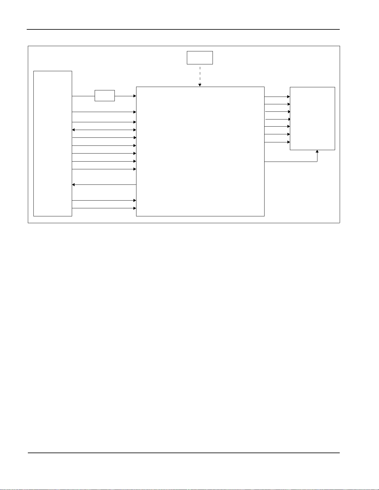
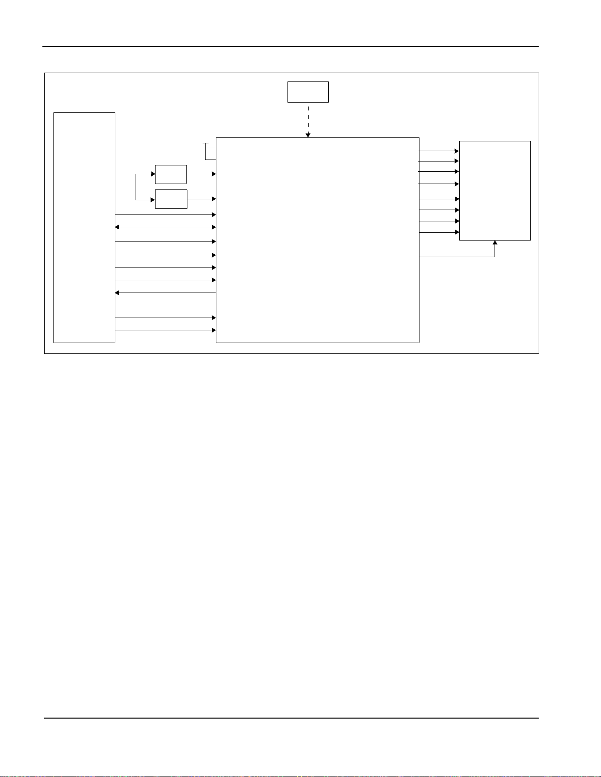
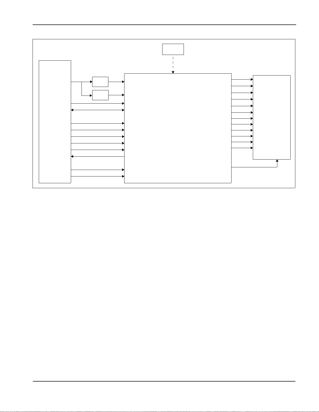
3 Typical System Implementation Diagrams
.
Oscillator
Generic #1
BUS
A[27:17]
A[16:0]
D[15:0]
WE0#
WE1#
RD0#
RD1#
WAIT#
BUSCLK
RESET#
CS#
IO V
DD
Decoder
BS#
M/R#
CS#
AB[16:0]
DB[15:0]
WE0#
WE1#
RD#
RD/WR#
WAIT#
CLKI
RESET#
S1D13708
CLKI2
Figure 3-1 Typical System Diagram (Generic #1 Bus)
.
Oscillator
FPDAT[15:0]
FPFRAME
FPLINE
FPSHIFT
DRDY
GPO0
D[15:0]
FPFRAME
FPLINE
FPSHIFT
MOD
16-bit
Single
LCD
Display
Bias Power
Generic #2
BUS
A[27:17]
CS#
A[16:0]
D[15:0]
WE#
BHE#
RD#
WAIT#
BUSCLK
RESET#
Decoder
IO V
DD
BS#
RD/WR#
M/R#
CS#
AB[16:0]
DB[15:0]
WE0#
WE1#
RD#
WAIT#
CLKI
RESET#
CLKI2
S1D13708
FPDAT[8:0]
FPFRAME
FPLINE
FPSHIFT
DRDY
GPO0
D[8:0]
FPFRAME
FPLINE
FPSHIFT
DRDY
9-bit
TFT
Display
Bias Power
Figure 3-2 Typical System Diagram (Generic #2 Bus)
Hardware Functional Specification S1D13708
Issue Date: 02/03/07 X39A-A-001-02
Page 26
Page 20 Epson Research and Development
Vancouver Design Center
.
Oscillator
SH-4
BUS
A[25:17]
CSn#
A[16:0]
D[15:0]
WE0#
WE1#
BS#
RD/WR#
RD#
RDY#
CKIO
RESET#
Decoder
M/R#
CS#
AB[16:0]
DB[15:0]
WE0#
WE1#
BS#
RD/WR#
RD#
WAIT#
CLKI
RESET#
CLKI2
S1D13708
Figure 3-3 Typical System Diagram (Hitachi SH-4 Bus)
FPDAT15
FPDAT12
FPDAT[9:0]
FPFRAME
FPLINE
FPSHIFT
DRDY
GPO0
D11
D10
D[9:0]
FPFRAME
FPLINE
FPSHIFT
DRDY
12-bit
TFT
Display
Bias Power
S1D13708 Hardware Functional Specification
X39A-A-001-02 Issue Date: 02/03/07
Page 27

Epson Research and Development Page 21
Vancouver Design Center
.
Oscillator
SH-3
BUS
A[25:17]
CSn#
A[16:0]
D[15:0]
WE0#
WE1#
BS#
RD/WR#
RD#
WAIT#
CKIO
RESET#
Decoder
M/R#
CS#
AB[16:0]
DB[15:0]
WE0#
WE1#
BS#
RD/WR#
RD#
WAIT#
CLKI
RESET#
CLKI2
S1D13708
Figure 3-4 Typical System Diagram (Hitachi SH-3 Bus)
FPDAT[17:0]
FPFRAME
FPLINE
FPSHIFT
DRDY
GPO0
D[17:0]
FPFRAME
FPLINE
FPSHIFT
DRDY
18-bit
TFT
Display
Bias Power
Hardware Functional Specification S1D13708
Issue Date: 02/03/07 X39A-A-001-02
Page 28
Page 22 Epson Research and Development
Vancouver Design Center
.
Oscillator
MC68K #1
BUS
A[23:17]
FC0, FC1
A[16:1]
D[15:0]
LDS#
UDS#
AS#
R/W#
DTACK#
Decoder
Decoder
IO V
DD
RD#
WE0#
M/R#
CS#
AB[16:1]
DB[15:0]
AB0
WE1#
BS#
RD/WR#
WAIT#
CLKI2
S1D13708
FPDAT[17:0]
FPFRAME
FPLINE
FPSHIFT
GPIO0
GPIO1
GPIO2
GPIO3
GPO0
D[17:0]
SPS
LP
CLK
PS
CLS
REV
SPL
18-bit
HR-TFT
Display
Bias Power
CLK
RESET#
CLKI
RESET#
Figure 3-5 Typical System Diagram (MC68K # 1, Motorola 16-Bit 68000)
S1D13708 Hardware Functional Specification
X39A-A-001-02 Issue Date: 02/03/07
Page 29
Epson Research and Development Page 23
Vancouver Design Center
.
Oscillator
MC68K #2
BUS
A[31:17]
FC0, FC1
A[16:0]
D[31:16]
DS#
AS#
R/W#
SIZ1
SIZ0
DSACK1#
Decoder
Decoder
M/R#
CS#
AB[16:0]
DB[15:0]
WE1#
BS#
RD/WR#
RD#
WE0#
WAIT#
CLKI2
S1D13708
FPDAT[17:0]
FPFRAME
FPLINE
FPSHIFT
DRDY
GPIO0
GPIO1
GPIO2
GPIO3
GPIO4
GPIO5
GPIO6
D[17:0]
DY
LP
XSCL
GCP
XINH
YSCL
FR
FRS
RES
DD_P1
YSCLD
18-bit
D-TFD
Display
XSET (Bias Power)
CLK
RESET#
CLKI
RESET#
GPO0
Figure 3-6 Typical System Diagram (MC68K #2, Motorola 32-Bit 68030)
Hardware Functional Specification S1D13708
Issue Date: 02/03/07 X39A-A-001-02
Page 30

Page 24 Epson Research and Development
Vancouver Design Center
.
Oscillator
REDCAP2
BUS
A[21:17]
CSn
A[16:0]
D[15:0]
R/W
OE
EB1
EB0
CLK
RESET_OUT
*Note: CSn# can be any of CS0-CS4
Decoder
Figure 3-7 Typical System Diagram (Motorola REDCAP2 Bus)
IO V
DD
BS#
M/R#
CS#
AB[16:0]
DB[15:0]
RD/WR#
RD#
WE0#
WE1#
CLKI
RESET#
CLKI2
S1D13708
FPDAT[7:4]
FPSHIFT
FPFRAME
FPLINE
DRDY
GPO0
D[3:0]
FPSHIFT
FPFRAME
FPLINE
MOD
4-bit
Single
LCD
Display
Bias Power
S1D13708 Hardware Functional Specification
X39A-A-001-02 Issue Date: 02/03/07
Page 31

Epson Research and Development Page 25
Vancouver Design Center
.
Oscillator
MC68EZ328/
MC68VZ328
DragonBall
BUS
A[25:17]
Decoder
IO V
DD
BS#
RD/WR#
M/R#
CLKI2
FPDAT[7:0]
FPSHIFT
D[7:0]
FPSHIFT
8-bit
Single
LCD
Display
CS
A[16:0]
D[15:0]
n
CS#
AB[16:0]
DB[15:0]
FPFRAME
FPLINE
DRDY
S1D13708
LWE
UWE
OE
DTACK
CLKO
RESET
WE0#
WE1#
RD#
WAIT#
CLKI
RESET#
Figure 3-8 Typical System Diagram (Motorola MC68EZ328/MC68VZ328 “DragonBall” Bus)
Indirect
Interface
Mode 68
A[23:17]
FC0, FC1
BUSCLK
RESET#
VSS
Decoder
A0
D[15:0]
EBL
EBU
R/W#
AB[16:0]
RD#
BS#
CS#
M/R#
DB[15:0]
WE0#
WE1#
RD/WR#
CLKI
RESET#
XTAL0
XTAL1
S1D13708
GPO0
FPDAT[7:4]
FPSHIFT
FPFRAME
FPLINE
DRDY
GPO0
FPFRAME
FPLINE
MOD
D[3:0]
FPSHIFT
FPFRAME
FPLINE
MOD
Bias Power
4-bit
Single
LCD
Display
Bias Power
Figure 3-9 Typical System Diagram (Indirect Interface, Mode 68)
Hardware Functional Specification S1D13708
Issue Date: 02/03/07 X39A-A-001-02
Page 32

Page 26 Epson Research and Development
Vancouver Design Center
Indirect
Interface
Mode 80
BUSCLK
RESET#
A[23:17]
A0
D[15:0]
RDU#
WRL#
WRU#
Decoder
IO V
VSS
DD
BS#
AB[16:0]
CS#
M/R#
DB[15:0]
RD/WR#RDL#
RD#
WE0#
WE1#
CLKI
RESET#
XTAL0
XTAL1
S1D13708
FPDAT[7:4]
FPSHIFT
FPFRAME
FPLINE
DRDY
GPO0
D[3:0]
FPSHIFT
FPFRAME
FPLINE
MOD
4-bit
Single
LCD
Display
Bias Power
Figure 3-10 Typical System Diagram (Indirect Interface, Mode 80)
S1D13708 Hardware Functional Specification
X39A-A-001-02 Issue Date: 02/03/07
Page 33

Epson Research and Development Page 27
Vancouver Design Center
4 Pins
4.1 Pinout Diagram - PFBGA - 120pin
L
K
J
H
G
F
E
D
C
B
A
1234567891011
BOTTOM VIEW
Figure 4-1 Pinout Diagram - PFBGA 120-pin
Table 4-1: PFBGA 120-pin Mapping
COREVDD IOVDD AB6 AB2 DB7 DB4 DB0 WAIT# FPLINE GPIO5 IOVDD
L
K
J
H
G
F
E
D
C
B
A
AB7 AB5 AB4 AB3 COREVDD DB3 M/R# IOVDD GPIO6 GPIO4 COREVDD
AB10 AB9 AB8 AB1 DB6 DB2 BS# FPFRAME GPIO1 GPIO2 GPIO3
AB14 AB13 AB11 AB0 DB5 DB1 RD# COREVDD PWMOUT GPIO0 DRDY
XTAL0 IOVDD AB15 AB12 VSS VSS VSS GPO6 CLKI2 FPSHIFT CVOUT
COREVDD CLKI XTAL1 AB16 VSS VSS GPO2 GPO5 GPO7 IOVDD
DB11 DB10 DB8 VSS VSS VSS VSS CNF7 GPO1 G PO3 GPO4
DB15 DB14 DB12 DB9 FPDAT0 FPDAT6 FPDAT12 FPDAT16 CNF6 TESTEN GPO0
WE0# CS# DB13 FPDAT1 FPDAT4 FPDAT7 IOVDD FPDAT13 FPDAT17 CNF4 CNF5
COREVDD WE1# RD/WR# FPDAT2 COREVDD FPDAT8 FPDAT10 FPDAT14 CNF0 CNF2 CNF3
IOVDD RESET# IOVDD FPDAT3 FPDAT5 FPDAT9 FPDAT11 FPDAT15 CNF1 COREVDD IOVDD
1234567891011
Hardware Functional Specification S1D13708
Issue Date: 02/03/07 X39A-A-001-02
Page 34

Page 28 Epson Research and Development
Vancouver Design Center
4.2 Pinout Diagram - Die Form
Table 4-2: S1D13708 Pad Layout
VSS
IOVDD
CNF3
CNF4
CNF5
CNF6
CNF7
TESTEN
GPO0
GPO1
GPO2
GPO3
GPO4
GPO5
GPO6
GPO7
VSS
CLKI2
IOVDD
FPSHIFT
VSS
COREVDD
CVOUT
PWMOUT
GPO0
GPIO0
GPIO1
GPIO2
GPIO3
GPIO4
GPIO5
VSS
COREVDD
989796959493929190898887868584838281807978777675747372717069686766
COREVDD
VSS
CNF2
CNF1
CNF0
FPDAT17
FPDAT16
FPDAT15
FPDAT14
FPDAT13
FPDAT12
FPDAT11
FPDAT10
IOVDD
VSS
FPDAT9
FPDAT8
FPDAT7
FPDAT6
FPDAT5
COREVDD
VSS
FPDAT4
FPDAT3
FPDAT2
FPDAT1
FPDAT0
IOVDD
VSS
*CUT
IOVDD
VSS
99 65
100
101 87 57 63
102 88 56 62
103 89 55 61
104 90 54 60
105 91 53 59
106 92 52 58
107 93 51 57
108 94 50 56
109 95 49 55
110 96 48 54
111 97 47 53
112 98 46 52
113 99 45 51
114 100 44 50
115 101 43 49
116 102 42 48
117 103 41 47
118 104 40 46
119 105 39 45
120 106 38 44
121 107 37 43
122 108 36 42
123 109 35 41
124 110 34 40
125 111 33 39
126 112 32 38
127 113 31 37
128 114 30 36
129 35
130
8685848382818079787776757473727170696867666564636261605958
S1D13708
123456789
10111213141516171819202122232425262728
29
64
34
VSS
IOVDD
GPIO6
FPLINE
FPFRAME
*CUT
VSS
IOVDD
WAIT#
RD#
BS#
M/R#
DB0
DB1
DB2
DB3
DB4
DB5
DB6
DB7
VSS
COREVDD
AB0
AB1
AB2
AB3
AB4
AB5
AB6
AB7
VSS
COREVDD
123456789
VSS
WE1#
WE0#
RESET#
COREVDD
RD/WR#
1011121314151617181920212223242526272829303132
CS#
VSS
DB15
DB14
DB13
DB12
DB9
DB8
DB11
DB10
CLKI
VSS
AB16
AB15
XTAL1
XTAL0
IOVDD
AB14
COREVDD
33
AB9
AB8
AB13
AB12
AB11
AB10
VSS
IOVDD
S1D13708 Hardware Functional Specification
X39A-A-001-02 Issue Date: 02/03/07
Page 35

Epson Research and Development Page 29
Vancouver Design Center
4.3 Pin Descriptions
Key:
I = Input
O=Output
IO = Bi-Directional (Input/Output)
P=Power pin
PCLKI1 = CMOS/LVTTL schmitt input clock buffer
PIC = CMOS/LVTTL input buffer
PICS = CMOS/LVTTL input buffer with Schmitt input
POC8 = CMOS/LVTTL 8mA low noise output buffer
PBCC8 = CMOS/LVTTL bi-directional low noise buffer with 8mA CMOS output
PBCC8C = CMOS/LVTTL high-speed bi-directional low noise buffer with 8mA CMOS output
Hi-Z = High Impedance
POSC1 = Crystal oscillator IO cell
4.3.1 Host Interface
Table 4-3: Host Interface Pin Descriptions
Pin Name Type
AB0 I H4 PIC IOVDD 0
AB[16:1] I
PFBGA
Pin #
F4,G3,
G4,H1,
H2,H3,
J1,J2,
J3,J4,
K1,K2,
K3,K4,
L3,L4
Cell
PIC IOVDD 0
IO
Voltage
RESET
# State
Description
This input pin has multiple functions.
• For Generic #1, this pin inputs system address bit 0 (A0).
• For Generic #2, this pin inputs system address bit 0 (A0).
• For SH-3/SH-4, this pin inputs system address bit 0 (A0).
• For MC68K #1, this pin inputs the lower data strobe (LDS#).
• For MC68K #2, this pin inputs system address bit 0 (A0).
• For REDCAP2, this pin inputs system address bit 0 (A0).
• For DragonBall, this pin inputs system address bit 0 (A0).
• For Indirect (Mode 68), this pin is tied to V
• For Indirect (Mode 80), this pin is tied to VSS.
See Table 4-9: “Host Bus Interface Pin Mapping,” on page 39
summary.
System address bus bits 16-1.
• For Generic #1, these pins input system address bits 16-1.
• For Generic #2, these pins input system address bits 16-1.
• For SH-3/SH-4, these pins input system address bits 16-1.
• For MC68K #1, these pins input system address bits 16-1.
• For MC68K #2, these pins input system address bits 16-1.
• For REDCAP2, these pins input system address bits 16-1.
• For DragonBall, these pins input system address bits 16-1.
• For Indirect (Mode 68), these pins are tied to V
• For Indirect (Mode 80), these pins are tied to VSS.
SS
.
.
SS
for
Hardware Functional Specification S1D13708
Issue Date: 02/03/07 X39A-A-001-02
Page 36

Page 30 Epson Research and Development
Vancouver Design Center
Table 4-3: Host Interface Pin Descriptions
IO
Pin Name Type
PFBGA
Pin #
Cell
Voltage
C3,D1,
D2,D3,
D4,E1,
DB[15:0] IO
E2,E3,
H5,H6,
PBCC8 IOVDD Hi-Z
J5,J6,
K6,L5,
L6,L7
WE0# I C1 PIC IOVDD 1
RESET
# State
Description
Input data from the system data bus.
• For Generic #1, these pins are connected to D[15:0].
• For Generic #2, these pins are connected to D[15:0].
• For SH-3/SH-4, these pins are connected to D[15:0].
• For MC68K #1, these pins are connected to D[15:0].
• For MC68K #2, these pins are connected to D[31:16] for a 32bit device (e.g. MC68030) or D[15:0] for a 16-bit device (e.g.
MC68340).
• For REDCAP2, these pins are connected to D[15:0].
• For DragonBall, these pins are connected to D[15:0].
• For Indirect (Mode 68), these pins are connected to D[15:0].
• For Indirect (Mode 80), these pins are connected to D[15:0].
Unused pins should be tied to VSS. See Table 4-9: “Host Bus
Interface Pin Mapping,” on page 39
for summary.
This input pin has multiple functions.
• For Generic #1, this pin inputs the write enable signal for the
lower data byte (WE0#).
• For Generic #2, this pin inputs the write enable signal (WE#)
• For SH-3/SH-4, this pin inputs the write enable signal for data
byte 0 (WE0#).
• For MC68K #1, this pin must be tied to IO V
DD
• For MC68K #2, this pin inputs the bus size bit 0 (SIZ0).
• For REDCAP2, this pin inputs the byte enable signal for the
D[7:0] data byte (EB1
).
• For DragonBall, this pin inputs the byte enable signal for the
D[7:0] data byte (LWE).
• For Indirect (Mode 68), thi s pin inputs the byte enable signal for
the D[7:0] data byte (EBL).
• For Indirect (Mode 80), this pin inputs the write enable signal for
data byte 0 (WRL#).
See Table 4-9: “Host Bus Interface Pin Mapping,” on page 39
summary.
for
S1D13708 Hardware Functional Specification
X39A-A-001-02 Issue Date: 02/03/07
Page 37

Epson Research and Development Page 31
Vancouver Design Center
Table 4-3: Host Interface Pin Descriptions
IO
Pin Name Type
PFBGA
Pin #
Cell
Voltage
WE1# I B2 PIC IOVDD 1
CS# I C2 PIC IOVDD 1
M/R# I K7 PIC IOVDD 0
BS# I J7 PIC IOVDD 1
RESET
# State
Description
This input pin has multiple functions.
• For Generic #1, this pin inputs the write enable signal for the
upper data byte (WE1#).
• For Generic #2, this pin inputs the byte enable signal for the
high data byte (BHE#).
• For SH-3/SH-4, this pin inputs the write enable signal for data
byte 1 (WE1#).
• For MC68K #1, this pin inputs the upper data strobe (UDS#).
• For MC68K #2, this pin inputs the data strobe (DS#).
• For REDCAP2, this pin inputs the byte enable signal for the
D[15:8] data byte (EB0
).
• For DragonBall, this pin inputs the byte enable signal for the
D[15:8] data byte (UWE).
• For Indirect (Mode 68), this pi n in put s the byte enable signal for
the D[15:8] data byte (EBU).
• For Indirect (Mode 80), this pin inp uts the write enab le sig nal f or
data byte 1 (WRU#).
See Table 4-9: “Host Bus Interface Pin Mapping,” on page 39
for
summary.
Chip select input. See Table 4-9: “Host Bus Interface Pin Mapping,”
on page 39
for summary.
This input pin is used to select between the display buffer and
register address spaces of the S1D13708. M/R# is set high to
access the displa y b u ffer and low to access the registers. See Table
4-9: “Host Bus Interface Pin Mapping,” on page 39
for summary.
This input pin has multiple functions.
• For Generic #1, this pin must be tied to IO V
DD
.
• For Generic #2, this pin must be tied to IO VDD.
• For SH-3/SH-4, this pin inputs the bus start signal (BS#).
• For MC68K #1, this pin inputs the address strobe (AS#).
• For MC68K #2, this pin inputs the address strobe (AS#).
• For REDCAP2, this pin must be tied to IO V
DD
.
• For DragonBall, this pin must be tied to IO VDD.
• For Indirect (Mode 68), th is p in se lects the I ndirec t Interface For
Mode 68, this pin is tied to VSS.
• For Indirect (Mode 80), th is p in se lects the I ndirec t Interface For
Mode 80, this pin is tied to IO V
See Table 4-9: “Host Bus Interface Pin Mapping,” on page 39
DD
.
for
summary.
Hardware Functional Specification S1D13708
Issue Date: 02/03/07 X39A-A-001-02
Page 38

Page 32 Epson Research and Development
Vancouver Design Center
Table 4-3: Host Interface Pin Descriptions
IO
Pin Name Type
PFBGA
Pin #
Cell
Voltage
RD/WR# I B3 PIC IOVDD 1
RD# I H7 PIC IOVDD 1
RESET
# State
Description
This input pin has multiple functions.
• For Generic #1, this pin inputs th e rea d co mm an d for the upper
data byte (RD1#).
• For Generic #2, this pin must be tied to IO V
DD
.
• For SH-3/SH-4, this pin inputs the RD/WR# signal. The
S1D13708 needs this signal for early decode of the bus cycle.
• For MC68K #1, this pin inputs the R/W# signal.
• For MC68K #2, this pin inputs the R/W# signal.
• For REDCAP2, this pin inputs the R/W signal.
• For DragonBall, this pin must be tied to IO V
DD
.
• For Indirect (Mode 68), this pin inputs the R/W# signal.
• For Indirect (Mode 80, this pin inputs the read enable signal for
data byte 0 (RDL#).
See Table 4-9: “Host Bus Interface Pin Mapping,” on page 39
summary.
This input pin has multiple functions.
• For Generic #1, this pin inputs the read command for the lower
data byte (RD0#).
• For Generic #2, this pin inputs the read command (RD#).
• For SH-3/SH-4, this pin inputs the read signal (RD#).
• For MC68K #1, this pin must be tied to IO VDD.
• For MC68K #2, this pin inputs the bus size bit 1 (SIZ1).
• For REDCAP2, this pin inputs the output enable (OE
).
• For DragonBall, this pin inputs the output enable (OE).
• For Indirect (Mode 68), this pin is tied to V
SS
.
• For Indirect (Mode 80), this pin inp uts the read ena b le signal f or
data byte 1 (RDU#).
See Table 4-9: “Host Bus Interface Pin Mapping,” on page 39
summary.
for
for
S1D13708 Hardware Functional Specification
X39A-A-001-02 Issue Date: 02/03/07
Page 39

Epson Research and Development Page 33
Vancouver Design Center
Table 4-3: Host Interface Pin Descriptions
IO
Pin Name Type
PFBGA
Pin #
Cell
Voltage
WAIT# O L8 PBCC8C IOVDD Hi-Z
RESET# I A2 PICS IOVDD 0
RESET
# State
Description
During a data transfer, this output pin is driven active to force the
system to insert wait states. It is driven inactive to indicate the
completion of a data transfer. WAIT# is released to the high
impedance state af ter the data transfe r is complete. Its active polarit y
is configurable. See Table 4-8: “Summary of Power-On/Reset
Options,” on page 38.
• For Generic #1, this pin outputs the wait signal (WAIT#).
• For Generic #2, this pin outputs the wait signal (WAIT#).
• For SH-3 mode, this pin outputs the wait request signal
(WAIT#).
• For SH-4 mode, this pin outputs the device ready signal
(RDY#).
• For MC68K #1, this pin outputs the data transfer acknowledge
signal (DTACK#).
• For MC68K #2, this pin outputs the data transfer and size
acknowledge bit 1 (DSACK1#).
• For REDCAP2, this pin is unused (Hi-Z).
• For DragonBall, this pin outputs the data transfer acknowledge
signal (DTACK
).
• For Indirect (Mode 68), this pin is unused (Hi-Z).
• For Indirect (Mode 80), this pin is unused (Hi-Z).
See Table 4-9: “Host Bus Interface Pin Mapping,” on page 39 for
summary.
Active low input to set all internal registers to the default state and to
force all signals to their inactive states.
Hardware Functional Specification S1D13708
Issue Date: 02/03/07 X39A-A-001-02
Page 40

Page 34 Epson Research and Development
Vancouver Design Center
4.3.2 LCD Interface
Table 4-4: LCD Interface Pin Descriptions
IO
Pin Name Type
FPDAT[17:0] O
FPFRAME O J8 PBCC8 IOVDD 0
FPLINE O L9 PBCC8 IOVDD 0
FPSHIFT O G10 PBCC8 IOVDD 0
DRDY O H11 POC8 IOVDD 0
PFBGA
Pin #
A4,A5,
A6,A7,
A8,B4,
B6,B7,
B8,C4,
C5,C6,
C8,C9,
D5,D6,
D7,D8
Cell
PBCC8 IOVDD 0 Panel Data bits 17-0.
Voltage
RESET#
State
Description
This output pin has multiple functions.
•Frame Pulse
• SPS for Sharp HR-TFT
• DY for Epson D-TFD
• STV for TFT Type 2
•STV for Type 3
See Table 4-10: “LCD Interface Pin Mapping,” on page 40
summary.
This output pin has multiple functions.
•Line Pulse
• LP for Sharp HR-TFT
• LP for Epson D-TFD
• STB for TFT Type 2
• LP for Type 3
See Table 4-10: “LCD Interface Pin Mapping,” on page 40 for
summary.
This output pin has multiple functions.
• Shift Clock
• CLK for Sharp HR-TFT
• XSCL for Epson D-TFD
• CLK for TFT Type 2
•CPH for Type 3
See Table 4-10: “LCD Interface Pin Mapping,” on page 40
summary.
This output pin has multiple functions.
• Display enable (DRDY) for TFT panels
• 2nd shift clock (FPSHIFT2) for passive LCD with Format 1
interface
• GCP for Epson D-TFD
• INV for TFT T ype 2
• INV for TFT Type 3
• LCD backplane bias signal (MOD) for all other LCD panels
See Table 4-10: “LCD Interface Pin Mapping,” on page 40 for
summary.
for
for
S1D13708 Hardware Functional Specification
X39A-A-001-02 Issue Date: 02/03/07
Page 41

Epson Research and Development Page 35
Vancouver Design Center
Table 4-4: LCD Interface Pin Descriptions
IO
Pin Name Type
PFBGA
Pin #
Cell
Voltage
GPIO0 IO H10 PBCC8 IOVDD 0
GPIO1 IO J9 PBCC8 IOVDD 0
GPIO2 IO J10 PBCC8 IOVDD 0
GPIO3 IO J11 PBCC8 IOVDD 0
GPIO4 IO K10 PBCC8 IOVDD 0
RESET#
State
Description
This pin has multiple functions.
• PS for Sharp HR-TFT
• XINH for Epson D-TFD
• VCLK for TFT Type 2
• CPV for Type 3
• General purpose IO pin 0 (GPIO0)
• Hardware Video Invert
See Table 4-10: “LCD Interface Pin Mapping,” on page 40
for
summary.
This pin has multiple functions.
• CLS for Sharp HR-TFT
• YSCL for Epson D-TFD
• AP for TFT Type 2
•OE for Type 3
• General purpose IO pin 1 (GPIO1)
See Table 4-10: “LCD Interface Pin Mapping,” on page 40 for
summary.
This pin has multiple functions.
• REV for Sharp HR-TFT
• FR for Epson D-TFD
• POL for TFT Type 2
• POL for Type 3
• General purpose IO pin 2 (GPIO2)
See Table 4-10: “LCD Interface Pin Mapping,” on page 40
for
summary.
This pin has multiple functions.
• SPL for Sharp HR-TFT
• FRS for Epson D-TFD
• STH for TFT Type 2
• EIO for Type 3
• General purpose IO pin 3 (GPIO3)
See Table 4-10: “LCD Interface Pin Mapping,” on page 40
for
summary.
This pin has multiple functions.
• RES for Epson D-TFD
•VCOM for Type 3
• General purpose IO pin 4 (GPIO4)
See Table 4-10: “LCD Interface Pin Mapping,” on page 40
for
summary.
Hardware Functional Specification S1D13708
Issue Date: 02/03/07 X39A-A-001-02
Page 42

Page 36 Epson Research and Development
Vancouver Design Center
Table 4-4: LCD Interface Pin Descriptions
IO
Pin Name Type
PFBGA
Pin #
Cell
Voltage
GPIO5 IO L10 PBCC8 IOVDD 0
GPIO6 IO K9 PBCC8 IOVDD 0
PWMOUT O H9 PBCC8 IOVDD 0
CVOUT O G11 PBCC8 IOVDD 0
GPO0 O D11 POC8 IOVDD 0
GPO1 O E9 POC8 IOVDD 0
GPO2 O F8 POC8 IOVDD 0
GPO3 O E10 POC8 IOVDD 0
GPO4 O E11 POC8 IOVDD 0
GPO5 O F9 POC8 IOVDD 0
GPO6 O G8 POC8 IOVDD 0
GPO7 O F10 POC8 IOVDD 0
RESET#
State
Description
This pin has multiple functions.
• DD_P1 for Epson D-TFD
• XOEV for Type 3
• General purpose IO pin 5 (GPIO5)
See Table 4-10: “LCD Interface Pin Mapping,” on page 40
for
summary.
This pin has multiple functions.
• YSCLD for Epson D-TFD
• CMD for Type 3
• General purpose IO pin 6 (GPIO6)
See Table 4-10: “LCD Interface Pin Mapping,” on page 40
for
summary.
This output pin has multiple functions.
• PWM Clock ou tput
• General purpose output
This output pin has multiple functions.
• CV Pulse Output
• General purpose output
General Purpose Output (possibly used for controlling the LCD
power). It may also be us ed for the MOD control signal of the
Sharp HR-TFT panel.
General Purpose Output pin 1 (GPO1).
When used with a Type 3 panel this pin functions as PCLK1.
General Purpose Output pin 2 (GPO2).
When used with a Type 3 panel this pin functions as PCLK2.
General Purpose Output pin 3 (GPO3).
When used with a Type 3 panel this pin functions as XRESH.
General Purpose Output pin 4 (GPO4).
When used with a Type 3 panel this pin functions as XRESV.
General Purpose Output pin 5 (GPO5).
When used with a Type 3 panel this pin functions as XOHV.
General Purpose Output pin 6 (GPO6).
When used with a Type 3 panel this pin functions as XSTBY.
General Purpose Output pin 7 (GPO7).
When used with a Type 3 panel this pin functions as PMDE.
S1D13708 Hardware Functional Specification
X39A-A-001-02 Issue Date: 02/03/07
Page 43

Epson Research and Development Page 37
Vancouver Design Center
4.3.3 Clock Input
Table 4-5: Clock Input Pin Descriptions
IO
Pin Name Type
PFBGA
Pin #
Cell
Voltage
CLKI I F2 PCLK1 IOVDD —
CLKI2 I G9 PCLK1 IOVDD —
XTAL0 0 F3 POSC1 IOVDD —
XTAL1 I G1 POSC1 IOVDD —
RESET#
State
Description
Typically used as input clock source for bus clock and memory
clock.
Typically used as input clock source for pixel clock This pin must
be tied to V
when a crystal is not used.
SS
Crystal output. This pin must be le ft unconnec ted when a crysta l is
not used.
Crystal input. This pin must be tied to V
when a crystal is not
SS
used.
4.3.4 Miscellaneous
Table 4-6: Miscellaneous Pin Descriptions
Pin Name Type
PFBGA
Pin #
Cell
IO
Voltage
A9, B9,
CNF[7:0] I
B10, B11,
C10, C11,
PIC IOVDD —
D9, E8
TESTEN I D10 PIC IOVDD 0
4.3.5 Power And Ground
Table 4-7: Power And Ground Pin Descriptions
Pin Name Type
IOVDD P
COREVDD P
VSS P
PFBGA
Pin #
A1, A3,
A11, C7,
F11, G2,
K8,L2,
L11
A10, B1,
B5, F1,
H8, K5,
K11, L1
E4, E5,
E6, E7,
F5, F7,
G5, G6,
G7
Cell
P——IO V
P——Core V
P——V
IO
Voltage
RESET#
State
RESET#
State
Description
These inputs are used t o configure the S1D13708 - see Table
4-8: “Summary of Power-On/Reset Options,” on page 38.
Note: These pins are used for configuration of the
S1D13708 and must be connected directly to IO V
or VSS.
DD
Test Enable input used for production test only (has type 1 pulldown resistor with a typical value of 50Ω at 3.3V).
Description
pins.
DD
pins.
DD.
pins.
SS
Hardware Functional Specification S1D13708
Issue Date: 02/03/07 X39A-A-001-02
Page 44

Page 38 Epson Research and Development
Vancouver Design Center
4.4 Summary of Configuration Options
Table 4-8: Summary of Power-On/Reset Options
S1D13708
Configuration
Input
Select host bus interface as follows:
CNF4 CNF2 CNF1 CNF0 Host Bus
1000SH-4/SH-3 interface, Big Endian
0000SH-4/SH-3 interface, Little Endian
1001MC68K #1, Big Endian
0001Reserved
1010MC68K #2, Big Endian
0010Reserved
CNF4,CNF[2:0]
CNF3 Configure GPIO pins as inputs at power-on
CNF5 WAIT# is active high WAIT# is active low
BCLK Source (CLKI/XTAL) to BCLK divide select:
Note: XTAL should only be used when configured for Indirect Interface (CNF[2:0] = 111).
CNF[7:6]
1011Generic #1, Big Endian
0011Generic #1, Little Endian
1100Reserved
0100Generic #2, Little Endian
1101REDCAP2, Big Endian
0101Reserved
1110DragonBall (MC68EZ328/MC68VZ328), Big Endian
0110Reserved
1111Indirect Interface, Big Endian
0111Indirect Interface, Little Endian
CNF7 CNF6 BCLK Divide Ratio
00 1 : 1
01 2 : 1
10 3 : 1
11 4 : 1
10
Power-On/Reset State
Configure GPIO pins as o utp uts at po w er-o n (for u se
by HR-TFT/D-TFD/TFT Type 2/TFT Type 3 when
selected)
S1D13708 Hardware Functional Specification
X39A-A-001-02 Issue Date: 02/03/07
Page 45

Epson Research and Development Page 39
Vancouver Design Center
4.5 Host Bus Interface Pin Mapping
Table 4-9: Host Bus Interface Pin Mapping
S1D13708
Pin Name
Generic #1 Generic #2
Hitachi
SH-3 /SH-4
Motorola
MC68K #1
Motorola
MC68K #2
Motorola
REDCAP2
Motorola
MC68EZ328
MC68VZ328
DragonBall
/
Indirect
Interface
Mode 68
Indirect
Interface
Mode 80
AB[16:1] A[16:1] A[16:1] A[16:1] A[16:1] A[16:1] A[16:1] A[16:1] Connected to V
AB0 A0
1
A0 A0
DB[15:0] D[15:0] D[15:0] D[15:0] D[15:0] D[15:0]
CS# External Decode CSn# External Decode CSn
1
LDS# A0 A0
2
1
A0
1
Connected to V
D[15:0] D[15:0] D[15:0] D[15:0]
CSn External Decode
M/R# External Decode A0 A0
CLKI BUSCLK BUSCLK CKIO CLK CLK CLK CLKO BUSCLK BUSCLK
BS# Connected to IO V
RD/WR# RD1#
DD
Connected
to IO V
DD
BS# AS# AS# Connected to IO V
RD/WR# R/W# R/W# R/W
RD# RD0# RD# RD#
WE0# WE0# WE# WE0#
Connected
to IO V
DD
Connected
to IO V
DD
Connected
External
Decode
Connected
to IO V
OE OE
DD
DD
to V
R/W# RDL#
Connected
to V
SIZ0 EB1 LWE EBL WRL#
SS
SS
Connected
to IO V
WE1# WE1# BHE# WE1# UDS# DS# EB0 UWE EBU WRU#
WAIT# WAIT# WAIT#
RESET# RESET# RESET# RESET# RESET# RESET#
WAIT#/
RDY#
DTACK# DSACK1# N/A DTACK
RESET_OUT
RESET RESET# RESET#
N/A N/A
SS
SS
DD
RDU#
Note
1
A0 for these busses is not used internally by the S1D13708.
2
If the target MC68K bus is 32-bit, then these signals should be connected to D[31:16].
Hardware Functional Specification S1D13708
Issue Date: 02/03/07 X39A-A-001-02
Page 46

Page 40 Epson Research and Development
Vancouver Design Center
4.6 LCD Interface Pin Mapping
Table 4-10: LCD Interface Pin Mapping
Monochrome Passive
Pin Name
FPFRAME FPFRAME SPS DY STV STV FPFRAME
FPLINE FPLINE LP LP STB LP FPLINE
FPSHIFT FPSHIFT DCLK XSCL CLK CPH FPSHIFT
DRDY MOD FPSHIFT2 MOD DRDY
FPDAT0
FPDAT1
FPDAT2
FPDAT3
FPDAT4 D0 D4 D0 (R2)
FPDAT5 D1 D5 D1 (B1)
FPDAT6 D2 D6 D2 (G1)
FPDAT7 D3 D7 D3 (R1)
FPDAT8
FPDAT9
FPDAT10
FPDAT11
FPDAT12
FPDAT13
FPDAT14
FPDAT15
FPDAT16
FPDAT17
GPIO0 GPIO0 GPIO0 GPIO0 GPIO0 GPIO0 GPIO0 GPIO0 GPIO0 GPIO0 PS XINH VCLK CPV GPIO0
GPIO1 GPIO1 GPIO1 GPIO1 GPIO1 GPIO1 GPIO1 GPIO1 GPIO1 GPIO1 CLS YSCL AP OE GPIO1
GPIO2 GPIO2 GPIO2 GPIO2 GPIO2 GPIO2 GPIO2 GPIO2 GPIO2 GPIO2 REV FR POL POL GPIO2
GPIO3 GPIO3 GPIO3 GPIO3 GPIO3 GPIO3 GPIO3 GPIO3 GPIO3 GPIO3 SPL FRS STH EIO GPIO3
GPIO4 GPIO4 GPIO4 GPIO4 GPIO4 GPIO4 GPIO4 GPIO4 GPIO4 GPIO4
GPIO5 GPIO5 GPIO5 GPIO5 GPIO5 GPIO5 GPIO5 GPIO5 GPIO5 GPIO5
GPIO6 GPIO6 GPIO6 GPIO6 GPIO6 GPIO6 GPIO6 GPIO6 GPIO6 GPIO6
GPO0 GPO0 (General Purpose Output) MOD GPO0 GPO0 GPO0 GPO0
GPO1 GPO1 GPO1 PCLK1 GPO1
GPO2 GPO2 GPO2 PCLK2 GPO2
GPO3 GPO3 GPO3 XRESH GPO3
GPO4 GPO4 GPO4 XRESV GPO4
GPO5 GPO5 GPO5 XOHV GPO5
GPO6 GPO6 GPO6 XSTBY GPO6
GPO7 GPO7 GPO7 PMDE GPO7
CVOUT CVOUT CVOUT CVOUT CVOUT
PWMOUT PWMOUT PWMOUT PWMOUT PWMOUT
Panel
Single
4-bit 8-bit 9-bit 12-bit 18-bit 18-bit 18-bit 18-bit 18-b it 18-bit
driven 0 D0 driven 0 D0 (B5)
driven 0 D1 driven 0 D1 (R5)
driven 0 D2 driven 0 D2 (G4)
driven 0 D3 driven 0 D3 (B3)
driven 0 driven 0 driven 0 driven 0 driven 0 D4 (G3)
driven 0 driven 0 driven 0 driven 0 driven 0 D5 (B2)
driven 0 driven 0 driven 0 driven 0 driven 0 D6 (R2)
driven 0 driven 0 driven 0 driven 0 driven 0 D7 (G1)
driven 0 driven 0 driven 0 driven 0 driven 0 D12 (R3)
driven 0 driven 0 driven 0 driven 0 driven 0 D13 (G2)
driven 0 driven 0 driven 0 driven 0 driven 0 D14 (B1)
driven 0 driven 0 driven 0 driven 0 driven 0 D15 (R1)
driven 0 driven 0 driven 0 driven 0 driven 0 driven 0 driven 0 driven 0 B1 B1 B1 B1 B1 B1
driven 0 driven 0 driven 0 driven 0 driven 0 driven 0 driven 0 driven 0 B0 B0 B0 B0 B0 B0
4-bit
2
2
2
2
Color Passive Panel Color TFT Panel
Format 1
8-bit
D4 (R3)
D5 (G2)
D6 (B1)
D7 (R1)
Single
Format 2
8-bit
2
2
2
2
2
2
2
2
D0 (G3)
D1 (R3)
D2 (B2)
D3 (G2)
D4 (R2)
D5 (B1)
D6 (G1)
D7 (R1)
2
2
2
2
2
2
2
2
16-Bit
D0 (R6)
D1 (G5)
D2 (B4)
D3 (R4)
D8 (B5)
D9 (R5)
D10 (G4)
D11 (B3)
2
2
2
2
2
2
2
2
2
2
2
2
2
2
2
2
Generic TFT (TFT Type 1)
R2 R3 R5 R5 R5 R5 R5 R5
R1 R2 R4 R4 R4 R4 R4 R4
R0 R1 R3 R3 R3 R3 R3 R3
G2 G3 G5 G5 G5 G5 G5 G5
G1 G2 G4 G4 G4 G4 G4 G4
G0 G1 G3 G3 G3 G3 G3 G3
B2 B3 B5 B5 B5 B5 B5 B5
B1 B2 B4 B4 B4 B4 B4 B4
B0 B1 B3 B3 B3 B3 B3 B3
driven 0 R0 R2 R2 R2 R2 R2 R2
driven 0 driven 0 R1 R 1 R1 R1 R1 R1
driven 0 driven 0 R0 R 0 R0 R0 R0 R0
driven 0 G0 G2 G2 G2 G2 G2 G2
driven 0 driven 0 G1 G1 G1 G1 G1 G1
driven 0 driven 0 G0 G0 G0 G0 G0 G0
driven 0 B0 B2 B2 B2 B2 B2 B2
Sharp HR-
1
TFT
no connect GCP INV INV DRDY
GPIO4
(output only)
GPIO5
(output only)
GPIO6
(output only)
Epson
D-TFD
RES
DD_P1
YSCLD
TFT Type 2 TFT Type 3 TFT Type 4
1
GPIO4
(output only)
GPIO5
(output only)
GPIO6
(output only)
VCOM GPIO4
XOEV GPIO5
CMD GPIO6
Note
1
GPIO pins must be configured as outputs (CNF3 = 0 at RESET#) when TFT-Type 2,
TFT-Type 3, HR-TFT or D-TFD panels are selected.
2
These pin mappings use signal names commonly used for each panel type, however
signal names may differ between panel manufacturers. The values shown in brackets
represent the color components as mapped to the corresponding FPDATxx signals at
the first valid edge of FPSHIFT. For further FPDATxx to LCD interface mapping, see
Section 6.4, “Display Interface” on page 68.
S1D13708 Hardware Functional Specification
X39A-A-001-02 Issue Date: 02/03/07
Page 47

Epson Research and Development Page 41
Vancouver Design Center
5 D.C. Characteristics
Note
When applying Supply Voltages to the S1D13708, Core V
chip before, or simultaneously with IO V
, or damage to the chip may result.
DD
Table 5-1: Absolute Maximum Ratings (Preliminary - Subject to Change)
Symbol Parameter Rating Units
Core V
IO V
DD
V
IN
V
OUT
T
STG
T
SOL
DD
Supply Voltage VSS - 0.3 to 4.0 V
Supply Voltage VSS - 0.3 to 4.0 V
Input Voltage VSS - 0.3 to IO VDD + 0.5 V
Output Voltage VSS - 0.3 to IO VDD + 0.5 V
Storage Temperature -65 to 150 ° C
Solder Temperature/Time 260 for 10 sec. max at lead ° C
Table 5-2: Recommended Operating Conditions
must be applied to th e
DD
Symbol Parameter Condition Min Typ Max Units
Core V
IO V
DD
V
IN
T
OPR
DD
Supply Voltage VSS = 0 V 1.62 1.8 1.98 V
Supply Voltage VSS = 0 V 3.0 3.3 3.6 V
Input Voltage V
SS
IO V
DD
Operating Temperature 0 70 ° C
Table 5-3: Electrical Characteristics for VDD = 3.3V typical
Symbol Parameter Condition Min Typ Max Units
I
DDS
I
IZ
I
OZ
V
V
V
V
V
V
V
R
C
C
C
OH
OL
IH
IL
T+
TH1
PD
I
O
IO
Quiescent Current Quiescent Conditions 170 µA
Input Leakage Current -1 1 µA
Output Leakage Current -1 1 µA
High Level Output Voltage
Low Level Output Voltage
VDD = min.
= -8mA
I
OH
VDD = min.
= 8mA
I
OL
- 0.4 V
V
DD
0.4 V
High Level Input Voltage LVTTL Level, VDD = max 2.0 V
Low Level Input Voltage LVTTL Level, VDD = min 0.8 V
High Level Input Voltage LVTTL Schmitt 1.1 2.4 V
Low Level Input Voltage LVTTL Schmitt 0.6 1.8 V
Hysteresis Voltage LVTTL Schmitt 0.1 V
Pull Down Resistance VI = V
DD
20 50 120 kΩ
Input Pin Capacitance 10 pF
Output Pin Capacitance 10 pF
Bi-Directional Pin Capacitance 10 pF
V
Hardware Functional Specification S1D13708
Issue Date: 02/03/07 X39A-A-001-02
Page 48

Page 42 Epson Research and Development
Vancouver Design Center
6 A.C. Characteristics
Conditions: CORE VDD = 1.8V ± 10%
6.1 Clock Timing
6.1.1 Input Clocks
Clock Input Waveform
IO V
T
t
r
C
C
= 3.3V ± 10%
DD
= TBD ° C
A
and tf for all inputs must be < 5 nsec (10% ~ 90%)
= 50pF (Bus/MPU Interface)
L
= 0pF (LCD Panel Inter face)
L
t
PWL
t
f
90%
V
V
10%
t
PWH
IH
IL
t
r
T
OSC
Figure 6-1 Clock Input Requirements
Table 6-1: Clock Input Requirements for CLKI when CLKI to BCLK divide > 1
Symbol Parameter Min Max Units
f
OSC
T
OSC
t
PWH
t
PWL
Input Clock Frequency (CLKI) 100 MHz
Input Clock period (CLKI) 1/f
OSC
Input Clock Pulse Width High (CLKI) 4.5 ns
Input Clock Pulse Width Low (CLKI) 4.5 ns
Input Clock Fall Time (10% - 90%) 5 ns
t
f
Input Clock Rise Time (10% - 90%) 5 ns
t
r
ns
Note
Maximum internal requirements for clocks derived from CLKI must be considered
when determining the frequency of CLKI. See Secti on 6.1.2 , “Inter nal Clock s” on page
43 for internal clock requirements.
S1D13708 Hardware Functional Specification
X39A-A-001-02 Issue Date: 02/03/07
Page 49

Epson Research and Development Page 43
Vancouver Design Center
Table 6-2: Clock Input Requirements for CLKI when CLKI to BCLK divide = 1
Symbol Parameter Min Max Units
f
OSC
T
t
PWH
t
PWL
OSC
Input Clock Frequency (CLKI) 66 MHz
Input Clock period (CLKI) 1/f
OSC
Input Clock Pulse Width High (CLKI) 3 ns
Input Clock Pulse Width Low (CLKI) 3 ns
Input Clock Fall Time (10% - 90%) 5 ns
t
f
Input Clock Rise Time (10% - 90%) 5 ns
t
r
ns
Note
Maximum internal requirements for clocks derived from CLKI must be considered
when determining the frequency of CLKI. See Section 6.1.2, “Internal Clocks” on page
43 for internal clock requirements.
Table 6-3: Clock Input Requirements for CLKI2
Symbol Parameter Min Max Units
f
OSC
T
t
PWH
t
PWL
OSC
Input Clock Frequency (CLKI2) 66 MHz
Input Clock period (CLKI2) 1/f
OSC
Input Clock Pulse Width High (CLKI2) 3 ns
Input Clock Pulse Width Low (CLKI2) 3 ns
Input Clock Fall Time (10% - 90%) 5 ns
t
f
Input Clock Rise Time (10% - 90%) 5 ns
t
r
Note
Maximum internal requirements for clocks derived from CLKI2 must be considered
when determining the fre quency of CLKI2. See Se ction 6.1.2, “In ternal Clocks ” on page
43 for internal clock requirements.
6.1.2 Internal Clocks
Table 6-4: Internal Clock Requirements
Symbol Parameter Min Max Units
f
BCLK
f
MCLK
f
PCLK
f
PWMCLK
f
XTAL
Bus Clock frequency 66 MHz
Memory Clock frequency 50 MHz
Pixel Clock frequency 50 MHz
PWM Clock frequency 66 MHz
XTAL Clock frequency 12 MHz
ns
Note
For further information on internal clocks, refer to Section 7, “Clocks” on page 112.
Hardware Functional Specification S1D13708
Issue Date: 02/03/07 X39A-A-001-02
Page 50

Page 44 Epson Research and Development
Vancouver Design Center
6.2 CPU Interface Timing
The following section includes CPU interface AC Timing. These timings are based on IO
V
= 3.3V and Core VDD = 1.8V.
DD
6.2.1 Generic #1 Interface Timing
T
CLK
CLK
A[16:1], M/R#
CS#
WE0#, WE1#, RD0#, RD1#
WAIT#
D[15:0] (write)
D[15:0] (read)
t3
t8
t5
t9
t13
t4
t6
t7
t11
t14
t10
t15
Figure 6-2 Generic #1 Interface Timing
Note
The above diagram assumes that WAIT# is used and that MCLK = BCLK.
S1D13708 Hardware Functional Specification
X39A-A-001-02 Issue Date: 02/03/07
Page 51

Epson Research and Development Page 45
Vancouver Design Center
Table 6-5: Generic #1 Interface Timing
Symbol Parameter Min Max Unit
f
CLK
T
CLK
t7a WAIT# asserted for MCLK = BCLK 8 T
t7b WAIT# asserted for MCLK = BCLK
t7c WAIT# asserted for MCLK = BCLK
t7d WAIT# asserted for MCLK = BCLK
t10 Rising edge of either RD0#, RD1# or WE0#, WE1# to WAIT# high impedance 3 8 ns
t11
t12 D[15:0] hold from WAIT# rising edge (write cycle) 0 ns
t13 RD0#, RD1# falling edge to D[15:0] driven (read cycle) 4 11 ns
t14 WAIT# rising edge to D[15:0] valid (read cycle) 2 ns
t15 RD0#, RD1# rising edge to D[15:0] high impedance (read cycle) 3 9 ns
1. t11 is the delay from when data is placed on the bus until the data is latched into the write buffer.
Bus Clock frequency 50 MHz
Bus Clock period 1/f
A[16:0], M/R# setup to first CLK rising edge where CS# = 0 and either RD0#,
t3
RD1# = 0 or WE0#, WE1# = 0
CLK
1ns
ns
t4 A[16:0], M/R# hold from either RD0#, RD1# or WE0#, WE1# rising edge 0 ns
t5 CS# setup to CLK rising edge 1 ns
t6 CS# hold from either RD0#, RD1# or WE0#, WE1# rising edge 0 ns
÷ 2
÷ 3
÷ 4
13 T
17 T
20 T
CLK
CLK
CLK
CLK
t8 RD0#, RD1#, WE0#, WE1# setup to CLK rising edge 1 ns
t9 Falling edge of either RD0#, RD1# or WE0#, WE1# to WAIT# driven low 5 12 ns
D[15:0] setup to third CLK rising edge where CS# = 0 and WE0#, WE1# = 0
(write cycle) (see note 1)
1ns
Hardware Functional Specification S1D13708
Issue Date: 02/03/07 X39A-A-001-02
Page 52

Page 46 Epson Research and Development
Vancouver Design Center
6.2.2 Generic #2 Interface Timing
T
CLK
BUSCLK
A[16:1], M/R#, BHE#
CS#
RD#, WE#
WAIT#
D[15:0] (write)
D[15:0] (read)
t3
t5
t4
t6
t8
t9
t7
t10
t11
t13
t14
t15
Figure 6-3 Generic #2 Interface Timing
S1D13708 Hardware Functional Specification
X39A-A-001-02 Issue Date: 02/03/07
Page 53

Epson Research and Development Page 47
Vancouver Design Center
Table 6-6: Generic #2 Interface Timing
Symbol Parameter Min Max Unit
f
BUSCLK
T
BUSCLK
t7a WAIT# asserted for MCLK = BCLK 8 T
t7b WAIT# asserted for MCLK = BCLK ÷ 213T
t7c WAIT# asserted for MCLK = BCLK ÷ 315T
t7d WAIT# asserted for MCLK = BCLK ÷ 421T
t10 Rising edge of either RD# or WE# to WAIT# high impedance 3 8 ns
t11
t12 D[15:0] hold from WAIT# rising edge (write cycle) 0 ns
t13 RD# falling edge to D[15:0] driven (read cycle) 5 11 ns
t14 WAIT# rising edge to D[15:0] valid (read cycle) 2 ns
t15 Rising edge of RD# to D[15:0] high impedance (read cycle) 3 9 ns
Bus Clock frequency 50 MHz
Bus Clock period 1/f
A[16:0], M/R#, BHE# setup to first BUSCLK rising edge where CS# = 0 and
t3
either RD# = 0 or WE# = 0
BUSCLK
1ns
ns
t4 A[16:0], M/R#, BHE# hold from either RD# or WE# rising edge 0 ns
t5 CS# setup to BUSCLK rising edge 1 ns
t6 CS# hold from either RD# or WE# rising edge 0 ns
BUSCLK
BUSCLK
BUSCLK
BUSCLK
t8 RD# or WE# setup to BUSCLK rising edge 1 ns
t9 Falling edge of either RD# or WE# to WA IT# driven low 5 12 ns
D[15:0] setup to third BUSCLK rising edge where CS# = 0 and WE# = 0
(write cycle) (see note 1)
1ns
1. t11 is the delay from when data is placed on the bus until the data is latched into the write buffer.
Hardware Functional Specification S1D13708
Issue Date: 02/03/07 X39A-A-001-02
Page 54

Page 48 Epson Research and Development
Vancouver Design Center
6.2.3 Hitachi SH-4 Interface Timing
T
CKIO
CLKI
A[16:1], RD/WR#, M/R#
BS#
CSn#
WEn#, RD#
RDY
D[15:0] (write)
D[15:0] (read)
t13
t4
t8
t14
t3
t6
t5
t7
t11
t12
t9
t15
t10
t17
t16
t18
Figure 6-4 Hitachi SH-4 Interface Timing
S1D13708 Hardware Functional Specification
X39A-A-001-02 Issue Date: 02/03/07
Page 55

Epson Research and Development Page 49
Vancouver Design Center
Table 6-7: Hitachi SH-4 Interface Timing
Symbol Parameter Min Max Unit
f
CKIO
T
CKIO
t3
t4
t5
t6
t7
t8
t9a
t9b
t9c
t9d
t10
t11
t12
t13
t14
t15
t16
t17
t18
Clock frequency
Clock period
A[16:0], M/R#, RD/WR# setup to CKIO
A[16:0], M/R#, RD/WR# hold from CSn#
BS# setup
BS# hold
CSn# setup
CSn# high setup to CKIO
RDY asserted for MCLK = BCLK (max. MCLK = 50MHz)
RDY asserted for MCLK = BCLK ÷ 2
RDY asserted for MCLK = BCLK ÷ 3
RDY asserted for MCLK = BCLK ÷ 4
Falling edge RD# to D[15:0] driven (read cycle)
Falling edge CSn# to RDY# driven high
CKIO to RDY# low
CSn# high to RDY# high
Falling edge CKIO to RDY# high impedance
nd
D[15:0] setup to 2
CKIO after BS# (write cycle) (see note 1)
D[15:0] hold (write cycle)
RDY# falling edge to D[15:0] valid (read cycle)
Rising edge RD# to D[15:0] high impedance (read cycle)
1/f
CKIO
1ns
0ns
1ns
5ns
1ns
2ns
49ns
49ns
514ns
512ns
410ns
0ns
0ns
39ns
66 MHz
ns
7T
14 T
16 T
23 T
CKIO
CKIO
CKIO
CKIO
2ns
1. t15 is the delay from when data is placed on the bus until the data is latched into the write buffer.
Note
Minimum one software WA IT state is required.
Hardware Functional Specification S1D13708
Issue Date: 02/03/07 X39A-A-001-02
Page 56

Page 50 Epson Research and Development
Vancouver Design Center
6.2.4 Hitachi SH-3 Interface Timing
T
CKIO
CKIO
A[16:1], RD/WR#, M/R#
BS#
CSn#
WEn#, RD#
WAIT#
D[15:0] (write)
D[15:0] (read)
t3
t6
t5
t7
t12
t13
t8
t4
t11
t9
t14
t10
t16
t15
t17
Figure 6-5 Hitachi SH-3 Interface Timing
S1D13708 Hardware Functional Specification
X39A-A-001-02 Issue Date: 02/03/07
Page 57

Epson Research and Development Page 51
Vancouver Design Center
Table 6-8: Hitachi SH-3 Interface Timing
Symbol Parameter Min Max Unit
f
CKIO
T
CKIO
t3
t4
t5
t6
t7
t8
t9a
t9b
t9c
t9d
t10
t11
t12
t13
t14
t15
t16
t17
Bus Clock frequency
Bus Clock period
A[16:0], M/R#, RD/WR# setup to CKIO
CSn# high setup to CKIO
BS# setup
BS# hold
CSn# setup
A[16:0], M/R#, RD/WR# hold from CS#
WAIT# asserted for MCLK = BCLK (max. MCLK = 50MHz)
WAIT# asserted for MCLK = BCLK ÷ 2
WAIT# asserted for MCLK = BCLK ÷ 3
WAIT# asserted for MCLK = BCLK ÷ 4
Falling edge RD# to D[15:0] driven (read cycle)
Rising edge CSn# to WAIT# high impedance
Falling edge CSn# to WAIT# driven low
CKIO to WAIT# delay
nd
D[15:0] setup to 2
CKIO after BS# (write cycle) (see note 1)
D[15:0] hold (write cycle)
WAIT# rising edge to D[15:0] valid (read cycle)
Rising edge RD# to D[15:0] high impedance (read cycle)
1/f
CKIO
1ns
1ns
0ns
5ns
1ns
0ns
49ns
37ns
411ns
514ns
0ns
0ns
39ns
66 MHz
ns
6T
13 T
15 T
23 T
CKIO
CKIO
CKIO
CKIO
2ns
1. t14 is the delay from when data is placed on the bus until the data is latched into the write buffer.
Note
Minimum one software WA IT state is required.
Hardware Functional Specification S1D13708
Issue Date: 02/03/07 X39A-A-001-02
Page 58

Page 52 Epson Research and Development
Vancouver Design Center
6.2.5 Motorola MC68K #1 Interface Timing (e.g. MC68000)
T
CLK
CLK
A[16:1], R/W#, M/R#
CS#
AS#
UDS#, LDS#, (A0)
DTACK#
D[15:0] (write)
D[15:0] (read)
t3
t13
t15
t5
t8
t10
t4
t6
t9
t11
t12
t16
t7
t18
t17
t19
t20
t21
Figure 6-6 Motorola MC68K #1 Interface Timing
S1D13708 Hardware Functional Specification
X39A-A-001-02 Issue Date: 02/03/07
Page 59

Epson Research and Development Page 53
Vancouver Design Center
Table 6-9: Motorola MC68K #1 Interface Timing
Symbol Parameter Min Max Unit
f
CLK
T
t7a DTACK# asserted for MCLK = BCLK 8 T
t7b DTACK# asserted for MCLK = BCLK ÷ 213T
t7c DTACK# asserted for MCLK = BCLK ÷ 317T
t7d DTACK# asserted for MCLK = BCLK
t10 UDS#/LDS# setup to CLK rising edge while CS#, AS#, UDS#/LDS# = 0 1 ns
t11 UDS#/LDS# high setup to CLK rising edge 1 ns
t12 First CLK rising edge where AS# = 1 to DTACK# high impedance 3 10 ns
t13 R/W# setup to CLK rising edge before all CS#, AS#, UDS# and/or LDS# = 0 1 ns
t15 AS# = 0 and CS# = 0 to DTACK# driven high 4 10 ns
t16 AS# rising edge to DTACK# rising edge 5 14 ns
t17
t18 D[15:0] hold from DTACK# falling edge (write cycle) 0 ns
t19 UDS# = 0 and/or LDS# = 0 to D[15:0] driven (read cycle) 3 9 ns
t20 DTACK# falling edge to D[15:0] valid (read cycle) 0 ns
t21 UDS#, LDS# rising edge to D[15:0] high impedance (read cycle) 3 4 ns
Bus Clock Frequency 50 MHz
Bus Clock period 1/f
CLK
A[16:1], R/W#, M/R# setup to first CLK rising edge where CS# = 0,
t3
AS# = 0, UDS# = 0, and LDS# = 0
CLK
1ns
ns
t4 A[16:1], M/R# hold from AS# rising edge 0 ns
t5 CS# setup to CLK rising edge w hile CS#, A S#, UDS#/LDS# = 0 1 ns
t6 CS# hold from AS# rising edge 0 ns
÷ 423T
t8 AS# setup to CLK rising edge while CS#, AS#, UDS#/LDS# = 0 1 ns
t9 AS# setup to CLK rising edge 1 ns
D[15:0] valid to third CLK rising edge where CS# = 0, AS# = 0 and either
UDS# = 0 or LDS# = 0 (write cycle) (see note 1)
1ns
CLK
CLK
CLK
CLK
1. t17 is the delay from when data is placed on the bus until the data is latched into the write buffer.
Hardware Functional Specification S1D13708
Issue Date: 02/03/07 X39A-A-001-02
Page 60

Page 54 Epson Research and Development
Vancouver Design Center
6.2.6 Motorola MC68K #2 Interface Timing (e.g. MC68030)
T
CLK
CLK
A[16:1], R/W#, M/R#, SIZ[1:0]
CS#
AS#
UDS#, LDS#, (A0)
DSACK1#
D[31:16] (write)
D[31:16] (read)
t3
t13
t15
t5
t8
t10
t4
t6
t9
t11
t12
t16
t7
t18
t17
t19
t20
t21
Figure 6-7 Motorola MC68K #2 Interface Timing
S1D13708 Hardware Functional Specification
X39A-A-001-02 Issue Date: 02/03/07
Page 61

Epson Research and Development Page 55
Vancouver Design Center
Table 6-10: Motorola MC68K #2 Interface Timing
Symbol Parameter Min Max Unit
f
CLK
T
t7a DSACK1# asserted for MCLK = BCLK 8 T
t7b DSACK1# asserted for MCLK = BCLK ÷ 213T
t7c DSACK1# asserted for MCLK = BCLK ÷ 317T
t7d DSACK1# asserted for MCLK = BCLK
t10 DS# falling edge to CLK rising edge 4 ns
t11 DS# setup to CLK rising edge 4 ns
t12 First CLK where AS# = 1 to DSACK1# high impedance 2 28 ns
t13 R/W# setup to CLK rising edge before all CS# = 0, AS# = 0, and DS# = 0 1 ns
t15 AS# = 0 and CS# = 0 to DSACK1# rising edge 3 10 ns
t16 AS# rising edge to DSACK1# rising edge 5 14 ns
t17
t18 D[31:16] hold from falling edge of DSACK1# (write cycle) 0 ns
t19 DS# falling edge to D[31:16] driven (read cycle) 5 14 ns
t20 DSACK1# falling edge to D[31:16] valid (read cycle) 0 ns
t21 DS# rising edge to D[31:16] invalid/high impedance (read cycle) 3 10 ns
Bus Clock frequency 50 MHz
Bus Clock period 1/f
CLK
A[16:0], SIZ[1:0], M/R# setup to first CLK rising edge where
t3
CS# = 0, AS# = 0, DS# = 0
CLK
4ns
ns
t4 A[16:0], SIZ[1:0], M/R#, R/W# hold from AS# rising edge 0 ns
t5 CS# setup to CLK rising edge 3 ns
t6 CS# hold from AS# rising edge 0 ns
÷ 422T
t8 AS# falling edge to CLK rising edge 4 ns
t9 AS# rising edge to CLK rising edge 4 ns
D[31:16] valid to third CLK rising edge where CS# = 0, AS# = 0, and DS# = 0
(write cycle) (see note 1)
1ns
CLK
CLK
CLK
CLK
1. t17 is the delay from when data is placed on the bus until the data is latched into the write buffer.
Hardware Functional Specification S1D13708
Issue Date: 02/03/07 X39A-A-001-02
Page 62

Page 56 Epson Research and Development
Vancouver Design Center
6.2.7 Motorola REDCAP2 Inte rface Timing
T
CLK
CLK
A[16:1], R/W#, M/R#, CS#
EBO#, EB1# (write)
D[15:0] (write)
EB0#, EB1#, OE#
D[15:0] (read)
t3
t6
t8
t10
t13
t12
Note: CSn# may be any of CS0# - CS4#.
Figure 6-8 Motorola REDCAP2 Interface Timing
t4
t5
t7
t9
t11
t14
S1D13708 Hardware Functional Specification
X39A-A-001-02 Issue Date: 02/03/07
Page 63

Epson Research and Development Page 57
Vancouver Design Center
Table 6-11: Motorola REDCAP2 Interface Timing
Symbol Parameter Min Max Units
f
CLK
T
CLK
t3
t4
t5a
t5b
t5c
t5d
t6
t7
t8
t9
t10
t11
t12
t13a
t13b
t13c
t13d
t14
Bus Clock frequency
Bus Clock perio d
A[16:0], M/R#, R/W
A[16:0], M/R#, R/W
asserted fo r MCLK = BCLK
CSn
asserted fo r MCLK = BCLK ÷ 2
CSn
asserted fo r MCLK = BCLK ÷ 3
CSn
asserted fo r MCLK = BCLK ÷ 4
CSn
, EB1 asserted to CLK rising edge (write cycle)
EB0
, EB1 de-asserted to CLK rising edge (write cycle)
EB0
, CSn setup to CLK rising edge
, CSn hold from CLK rising edge
D[15:0] input setup to 3rd CLK rising edge after EB0
(write cycle) (see note 1)
D[15:0] input hold from 3rd CLK rising edge after EB0
(write cycle)
, EB0, EB1 setup to CLK rising edge (read cycle)
OE
, EB0, EB1 hold to CLK rising edge (read cycle)
OE
D[15:0] output delay from OE
, EB0, EB1 falling edge
(read cycle)
1st CLK rising edge after EB0
or EB1 asserted low to D[15:0] valid for MCLK
= BCLK (read cycle)
1st CLK rising edge after EB0
or EB1 asserted low to D[15:0] valid for MCLK
= BCLK ÷ 2 (read cycle)
1st CLK rising edge after EB0
or EB1 asserted low to D[15:0] valid for MCLK
= BCLK ÷ 3 (read cycle)
1st CLK rising edge after EB0
or EB1 asserted low to D[15:0] valid for MCLK
= BCLK ÷ 4 (read cycle)
CLK rising edge to D[15:0] output in Hi-Z (read cycle)
or EB1 asserted low
or EB1 asserted low
1/f
CLK
1ns
0ns
8T
10 T
13 T
15 T
2ns
3ns
1ns
1ns
1ns
1ns
511ns
39ns
17 MHz
ns
CLK
CLK
CLK
CLK
5CLK + 16 ns
8CLK + 16 ns
9CLK + 16 ns
11CLK + 16 ns
1. t8 is the delay from when data is placed on the bus until the data is latched into the write buffer.
Hardware Functional Specification S1D13708
Issue Date: 02/03/07 X39A-A-001-02
Page 64

Page 58 Epson Research and Development
Vancouver Design Center
6.2.8 Motorola DragonBall Interface Timing with DTACK (e.g. MC68EZ328/MC 68 VZ3 28)
T
CLKO
CLKO
t3
A[16:1]
t4
CSX#
UWE#, LWE# (write)
OE# (read)
D[15:0] (write)
D[15:0] (read)
DTACK#
t6
t8
t10
t12
t14
t17
t16
t7
t9
t11
t13
t15
t19
t18
t5
Figure 6-9 Motorola DragonBall Interface with DTACK Timing
S1D13708 Hardware Functional Specification
X39A-A-001-02 Issue Date: 02/03/07
Page 65

Epson Research and Development Page 59
Vancouver Design Center
Table 6-12: Motorola DragonBall Interface with DTACK Timing
Symbol Parameter
f
CLKO
T
CLKO
t3
Bus Clock frequency 16 33 MHz
Bus Clock perio d
A[16:0] setup 1st CLKO when CSX = 0 and either UWE/LWE
or OE
= 0
t4 A[16:0] hold from CSX rising edge 0 0 ns
t5a DTACK asserted for MCLK = BCLK 8 8 T
t5b DTACK asserted for MCLK = BCLK ÷ 21313T
t5c DTACK asserted for MCLK = BCLK ÷ 31616T
t5d DTACK asserted for MCLK = BCLK ÷ 42222T
t6 CSX setup to CLKO rising edge 2 2 ns
t7 CSX rising edge to CLKO rising edge 2 2 ns
t8 UWE/LWE falling edge to CLKO rising edge 2 2 ns
t9 UWE
/LWE rising edge to CSX rising edge 0 0 ns
t10 OE falling edge to CLKO rising edge 2 2 ns
t11 OE hold from CSX rising edge 0 0 ns
t12
D[15:0] setup to 3rd CLKO when CSX
(write cycle) (see note 1)
t13 D[15:0] in hol d from CSX
t14 Falling edge of OE
to D[15:0] driven (read cycle) 4 10 4 10 ns
rising edge (write cycle) 0 0 ns
, UWE/LWE asserted
t15 CSX rising edge to D[15:0] output Hi-Z (read cycle) 3939 ns
t16 CSX falling edge to DTACK driven high 4 9 4 10 ns
t17 DTACK
falling edge to D[15:0] valid (read cycle) 0 0 ns
t18 CSX high to DTACK high 513514 ns
t19 CLKO rising edge to DTACK Hi-Z 49410ns
MC68EZ328 MC68VZ328
Min Max Min Max
1/f
CLKO
1/f
CLKO
Unit
ns
00 ns
CLKO
CLKO
CLKO
CLKO
01 ns
1. t12 is the delay from when data is placed on the bus until the data is latched into the write buffer.
Hardware Functional Specification S1D13708
Issue Date: 02/03/07 X39A-A-001-02
Page 66

Page 60 Epson Research and Development
Vancouver Design Center
6.2.9 Motorola DragonBall Interface Timing w/o DTACK (e.g. MC68EZ328/MC68VZ328)
T
CLKO
CLKO
A[16:1]
CSX#
t3
t6
t5
t4
t7
UWE#, LWE# (write)
OE# (read)
D[15:0] (write)
D[15:0] (read)
Figure 6-10 Motorola DragonBall Interface without DTACK# Timing
t8
t10
t12
t15
t14
t9
t11
t13
t16
S1D13708 Hardware Functional Specification
X39A-A-001-02 Issue Date: 02/03/07
Page 67

Epson Research and Development Page 61
Vancouver Design Center
Table 6-13: Motorola DragonBall Interface without DTACK Timing
Symbol Parameter
f
CLKO
T
CLKO
Bus Clock frequency 16 33 MHz
Bus Clock perio d
A[16:0] setup 1st CLKO when CSX = 0 and either UWE/LWE
t3
or OE
= 0
t4 A[16:0] hold from CSX rising edge 0 0 ns
CSX asserted for MCLK = BCLK
t5a
(CPU wait state register should be programmed to 4 wait
states)
asserted for MCLK = BCLK ÷ 2
CSX
t5b
(CPU wait state register should be programmed to 8 wait
states)
asserted for MCLK = BCLK ÷ 3
CSX
t5c
(CPU wait state register should be programmed to 10 wait
states)
t6 CSX setup to CLKO rising edge 2 2 ns
t7 CSX
rising edge setup to CLKO rising edge 2 2 ns
t8 UWE/LWE setup to CLKO rising edge 2 2 ns
t9 UWE/LWE rising edge to CSX rising edge 0 0 ns
t10 OE
setup to CLKO rising edge 2 2 ns
t11 OE hold from CSX rising edge 0 0 ns
t12
t13 CSX
D[15:0] setup to 3rd CLKO after CSX, UWE/LWE asserted
(write cycle) (see note 1)
rising edge to D[15:0] output Hi-Z (write cycle) 0 0 ns
t14 Falling edge of OE to D[15:0] driven (read cycle) 5 11 5 11 ns
t15a
t15b
t15c
1st CLKO rising edge after OE
D[15:0] valid for MCLK = BCLK (read cycle)
1st CLKO rising edge after OE
D[15:0] valid for MCLK = BCLK ÷ 2 (read cycle)
1st CLKO rising edge after OE and CSX asserted low to
D[15:0] valid for MCLK = BCLK ÷ 3 (read cycle)
and CSX asserted low to
and CSX asserted low to
t16 CSX rising edge to D[15:0] output Hi-Z (read cycle) 3 9 3 9 ns
MC68EZ328 MC68VZ328
Min Max Min Max
1/f
CLKO
1/f
CLKO
Unit
ns
00ns
77T
Not Supported
Not Supported
11 T
13 T
CLKO
CLKO
CLKO
11ns
6T
CLKO
Not Supported
Not Supported
+ 6 6T
9T
12T
CLKO
CLKO
CLKO
+ 6
+ 6
+ 6
ns
ns
ns
1. t12 is the delay from when data is placed on the bus until the data is latched into the write buffer.
Hardware Functional Specification S1D13708
Issue Date: 02/03/07 X39A-A-001-02
Page 68

Page 62 Epson Research and Development
Vancouver Design Center
6.2.10 Indirect Interface Timing (Mode 68)
T
BUSCLK
BUSCLK
A0, R/W#
CS#
EBU, EBL
D[15:0] (write)
D[15:0] (read)
t1
t2
t8
t3
t4
t5
t6
Figure 6-11 Indirect Interface Timing (Mode 68)
t9
t7
S1D13708 Hardware Functional Specification
X39A-A-001-02 Issue Date: 02/03/07
Page 69

Epson Research and Development Page 63
Vancouver Design Center
Table 6-14: Indirect Interface Timing (Mode 68)
Symbol Parameter Min Max Units
f
BUSCLK
T
BUSCLK
t1
t2
t3
t4
t5
t6a
t6b
t6c
t6d
t7
t8a
t8b
t8c
t8d
t8e
t9a
t9b
t9c
t9d
t9e
Bus Clock frequency
Bus Clock period
A0 / R/W# setup to (CS# | EBU
A0 / R/W# hold to (CS# | EBU
D[15:0] setup to (CS# | EBU
D[15:0] hold to (CS# | EBU
Falling edge of (CS# | EBL
Falling edge of (CS# | EBL
), (CS# | EBL) rising edge
) rising edge (write cycle)
) rising edge (write cycle)
) to D[15:0] driven (read cycle)
) to valid D[15:0] driven for MCLK = BCLK
(read cycle)
Falling edge of (CS# | EBL
) to valid D[15:0] driven for MCLK = BCLK/2
(read cycle)
Falling edge of (CS# | EBL
) to valid D[15:0] driven for MCLK = BCLK/3
(read cycle)
Falling edge of (CS# | EBL
) to valid D[15:0] driven for MCLK = BCLK/4
(read cycle)
Valid D[15:0] hold to (CS# | EBL
(CS# | EBU
(CS# | EBL
(CS# | EBL
(CS# | EBL
(CS# | EBL
(CS# | EBL
(CS# | EBU
(CS# | EBU
(CS# | EBU
(CS# | EBU
) High pulse width (write cycle)
) High pulse width for MCLK = BCLK (read cycle)
) High pulse width for MCLK = BCLK/2 (read cycle)
) High pulse width for MCLK = BCLK/3 (read cycle)
) High pulse width for MCLK = BCLK/4 (read cycle)
) Low pulse width (read turnaround)
) Low pulse width for MCLK = BCLK (write turnaround)
) Low pulse width for MCLK = BCLK/2 (write turnaround)
) Low pulse width for MCLK = BCLK/3 (write turnaround)
) Low pulse width for MCLK = BCLK/4 (write turnaround)
), (CS# | EBL) falling edge
) rising edge
1/f
BUSCLK
1ns
3ns
1T
4ns
2T
7.5 T
9.5 T
12.5 T
16.5 T
0.5 T
4T
8T
11 T
15 T
17 T
2.5 T
2.5 T
5.5 T
7.5 T
9.5 T
50 MHz
ns
BUSCLK
BUSCLK
BUSCLK
BUSCLK
BUSCLK
BUSCLK
BUSCLK
BUSCLK
BUSCLK
BUSCLK
BUSCLK
BUSCLK
BUSCLK
BUSCLK
BUSCLK
BUSCLK
BUSCLK
Note
Max frequency (f
Hardware Functional Specification S1D13708
Issue Date: 02/03/07 X39A-A-001-02
BUSCLK
) when using crystal oscillator is 12MHz.
Page 70

Page 64 Epson Research and Development
Vancouver Design Center
6.2.11 Indirect Interface Timing (Mode 80)
T
BUSCLK
BUSCLK
A[16:1], M/R#
CS# | WRn#, CS# | RDn#
t3
t10
t4
t11
D[15:0] (write)
D[15:0] (read)
t5
t7
Figure 6-12 Indirect Interface Timing (Mode 80)
t6
t9t8
S1D13708 Hardware Functional Specification
X39A-A-001-02 Issue Date: 02/03/07
Page 71

Epson Research and Development Page 65
Vancouver Design Center
Table 6-15: Indirect Interface Timing (Mode 80)
Symbol Parameter Min Max Units
f
BUSCLK
T
BUSCLK
t3
t4
t5
t6
t7
t8a
t8b
t8c
t8d
t9
t10a
t10b
t10c
t10d
t10e
t11a
t11b
t11c
t11d
t11e
Bus Clock frequency
Bus Clock period
A0 setup to (CS# | WRn#), (CS# | RDn#) falling edge
A0 hold to (CS# | WRn#), (CS# | RDn#) rising edge
D[15:0] setup to (CS# | WRn#) rising edge (write cycle)
D[15:0] hold to (CS# | WRn#) rising edge (write cycle)
Falling edge of (CS# | RDn#) to D[15:0] driven (read cycle)
Falling edge of (CS# | RDn#) to valid D[15:0] driven for MCLK = BCLK
(read cycle)
Falling edge of (CS# | RDn#) to valid D[15:0] driven for MCLK = BCLK/2
(read cycle)
Falling edge of (CS# | RDn#) to valid D[15:0] driven for MCLK = BCLK/3
(read cycle)
Falling edge of (CS# | RDn#) to valid D[15:0] driven for MCLK = BCLK/4
(read cycle)
Valid D[15:0] hold to (CS# | RDn#) rising edge
(CS# | WRn#) Low pulse width (write cycle)
(CS# | RDn#) Low pulse width for MCLK = BCLK (read cycle)
(CS# | RDn#) Low pulse width for MCLK = BCLK/2 (read cycle)
(CS# | RDn#) Low pulse width for MCLK = BCLK/3 (read cycle)
(CS# | RDn#) Low pulse width for MCLK = BCLK/4 (read cycle)
(CS# | RDn#) High pulse width (read turnaround)
(CS# | WRn#) High pulse width for MCLK = BCLK (write turnaround)
(CS# | WRn#) High pulse width for MC LK = BCLK/2 (write turnaround)
(CS# | WRn#) High pulse width for MC LK = BCLK/3 (write turnaround)
(CS# | WRn#) High pulse width for MC LK = BCLK/4 (write turnaround)
1/f
BUSCLK
1ns
3ns
1T
4ns
2T
7.5 T
10.5 T
13.5 T
15.5 T
0.5 T
4T
8T
11 T
15 T
17 T
2T
2.5 T
5.5 T
7.5 T
9.5 T
50 MHz
ns
BUSCLK
BUSCLK
BUSCLK
BUSCLK
BUSCLK
BUSCLK
BUSCLK
BUSCLK
BUSCLK
BUSCLK
BUSCLK
BUSCLK
BUSCLK
BUSCLK
BUSCLK
BUSCLK
BUSCLK
Note
Max frequency (f
Hardware Functional Specification S1D13708
Issue Date: 02/03/07 X39A-A-001-02
BUSCLK
) when using crystal oscillator is 12MHz.
Page 72

Page 66 Epson Research and Development
Vancouver Design Center
6.3 LCD Power Sequencing
6.3.1 Passive/TFT Power-On Sequence
GPO0*
Power Save
Mode Enable**
(REG[A0h] bit 0)
t2
LCD Signals***
*It is recommended to use the general purpose output pin GPO0 to control the LCD bias power.
**The LCD power-on sequence is activated by programming the Power Save Mode Enable bit (REG[A0h] bit 0) to 0.
***LCD Signals include: FPDAT[17:0], FPSHIFT, FPLINE, FPFRAME, and DRDY.
t1
Figure 6-13 Passive/TFT Power-On Sequence Timing
Table 6-16: Passive/TFT Power-On Sequence Timing
Symbol Parameter Min Max Units
t1
t2
LCD signals active to LCD bias active
Power Save Mode disabled to LCD signals active
1. t1 is controlled by software and must be determined from the bias power supply delay requirements of the panel
connected.
Note 1 Note 1
020ns
S1D13708 Hardware Functional Specification
X39A-A-001-02 Issue Date: 02/03/07
Page 73

Epson Research and Development Page 67
Vancouver Design Center
6.3.2 Passive/ TFT Power-Of f Seque nce
t1
GPO0*
Power Save
Mode Enable**
(REG[A0h] bit 0)
LCD Signals***
*It is recommended to use the general purpose output pin GPO0 to control the LCD bias power.
**The LCD power-off sequence is activated by programming the Power Save Mode Enable bit (REG[A0h] bit 0) to 1.
***LCD Signals include: FPDAT[17:0], FPSHIFT, FPLINE, FPFRAME, and DRDY.
Figure 6-14 Passive/TFT Power-Off Sequence Timing
t2
Table 6-17: Passive/TFT Power-Off Sequence Timing
Symbol Parameter Min Max Units
t1
t2
LCD bias deactivated to LCD signals inactive
Power Save Mode enabled to LCD signals low
1. t1 is controlled by software and must be determined from the bias power supply delay requirements of the panel
connected.
Note 1 Note 1
020ns
Hardware Functional Specification S1D13708
Issue Date: 02/03/07 X39A-A-001-02
Page 74

Page 68 Epson Research and Development
Vancouver Design Center
6.4 Display Interface
The timing parameters required to drive a flat panel display are shown below. Timing
details for each supported panel type are provided in the remainder of this section.
HT
HDPS
HPWHPS
VPS
VDPS
VPW
HDP
VT
VDP
Figure 6-15 Panel Timing Parameters
S1D13708 Hardware Functional Specification
X39A-A-001-02 Issue Date: 02/03/07
Page 75

Epson Research and Development Page 69
Vancouver Design Center
Table 6-18: Panel Timing Parameter Definition and Register Summary
Symbol Description Derived From Units
HT Horizontal Total ((REG[12h] bits 6-0) + 1) x 8
1
HDP
Horizontal Display Period
HDPS Horizontal Display Period Start Position
HPS FPLI NE Pulse Start Posi tio n (REG[23h] bits 1-0, REG[22h ] bits 7-0) + 1
HPW FPLINE Pulse Width (REG[20h] bits 6-0) + 1
VT Vertical Total (REG[19h] bits 1-0, REG[18h] bits 7-0) + 1
VDP Vertical Display Period (REG[1Dh] bits 1-0, REG[1Ch] bits 7-0) + 1
VDPS Vertical Display Period Start Position REG[1Fh] bits 1-0, REG[1Eh] bits 7-0
VPS FPFRAME Pulse Start Position REG[27h] bits 1-0, REG[26h] bits 7-0
VPW FPFRAME Pulse Width (REG[24h] bits 6-0) + 1
1. For passive panels, the HDP must be a minimum of 32 pixels and must be increased by multiples of 16.
For TFT panels, the HDP must be a minimum of 8 pixels and must be increased by multiples of 8.
2. The following formulas must be valid for all panel timings:
HDPS + HDP < HT
VDPS + VDP < VT
1
((REG[44h] bits 6-0) + 1) x 8
For STN panels: ((REG[17h] bits 1-0, R EG[ 16h] bits 7-0) + 22)
For TFT panels: ((REG[17h] bits 1-0, REG[16h] bits 7-0) + 5)
Lines (HT)
Ts
Hardware Functional Specification S1D13708
Issue Date: 02/03/07 X39A-A-001-02
Page 76

Page 70 Epson Research and Development
Vancouver Design Center
6.4.1 Generic STN Panel Timing
VT (= 1 Frame)
VPW
FPFRAME
VDP
FPLINE
1
(DRDY)
MOD
FPDAT[17:0]
FPLINE
FPSHIFT
MOD2(DRDY)
FPDAT[17:0]
1PCLK
HDPS
HT (= 1 Line)
HPWHPS
HDP
Figure 6-16 Generic STN Panel Timing
S1D13708 Hardware Functional Specification
X39A-A-001-02 Issue Date: 02/03/07
Page 77

Epson Research and Development Page 71
Vancouver Design Center
VT = Vertical Total = [(REG[19h] bits 1-0, REG[18h] bits 7-0) + 1] lines
VPS = FPFRAME Pulse Start Position = 0 lines, because [(REG[27h] bits 1-0, REG[26h] bits 7-0)] = 0
VPW = FPFRAME Pulse Width = [(REG[24h] bits 2-0) + 1] lines
VDPS = Vertical Display Period Start Position = 0 lines, because [(REG[1Fh] bits 1-0, REG[1Eh] bits 7-0)] = 0
VDP = Vertical Display Period = [(REG[1Dh] bits 1-0, REG[1Ch] bits 7-0) + 1] lines
HT = Horizontal Total = [((REG[12h] bits 6-0) + 1) x 8] pixels
HPS = FPLINE Pulse Start Position = [(REG[23h] bits 1-0, REG[22h] bits 7-0) + 1] pixels
HPW = FPLINE Pulse Width = [(REG[20h] bits 6-0) + 1] pixels
HDPS = Horizontal Display Period Start Position= 22 pixels, because [(REG[17h] bits 1-0, REG[16h] bits 7-0)] = 0
HDP = Horizontal Display Period = [((REG[14h] bits 6-0) + 1) x 8] pixels
*For passive panels, the HDP must be a minimum of 32 pixels and must be increased by multiples of 16.
*HPS must comply with the following formula:
HPS > HDP + 22
HPS + HPW < HT
*Panel Type Bits (REG[10h] bits 1-0) = 00b (STN)
*FPFRAME Pulse Polarity Bit (REG[24h] bit 23) = 1 (active high)
*FPLINE Pulse Polarity Bit (REG[20h] bit 7) = 1 (active high)
1
*MOD
*MOD
is the MOD signal when REG[11h] bits 5-0 = 0 (MOD toggles every FPFRAME)
2
is the MOD signal when REG[11h] bits 5-0 = n (MOD toggles every n FPLINE)
Hardware Functional Specification S1D13708
Issue Date: 02/03/07 X39A-A-001-02
Page 78

Page 72 Epson Research and Development
Vancouver Design Center
6.4.2 Single Monochrome 4-Bit Panel Timing
FPFRAME
FPLINE
DRDY (MOD)
FPDAT[7:4]
Invalid
LINE1 LINE2 LINE3 LINE4 LINE239 LINE240 LINE1 LINE2
FPLINE
DRDY (MOD)
FPSHIFT
FPDAT7
FPDAT6
FPDAT5
FPDAT4
* Diagram drawn with 2 FPLINE vertical blank per iod
Example timing for a 320x240 panel
Invalid
Invalid
Invalid
Invalid
1-1 1-5
1-2 1-6 1-318
1-3
1-4 1-8
Figure 6-17 Single Monochrome 4-Bit Panel Timing
VDP
HDP
1-7
VNDP
Invalid
1-317
1-319
1-320
HNDP
Invalid
Invalid
Invalid
Invalid
VDP = Vertical Display Period
= (REG[1Dh] bits 1:0, REG[1Ch] bits 7:0) + 1 Lines
VNDP = Vertical Non-Display Period
= VT - VDP
= (REG[19h] bits 1:0, REG[18h] bits 7:0) - (REG[1Dh] bits 1:0, REG[1Ch] bits 7:0) Lines
HDP = Horizontal Display Period
= ((REG[14h] bits 6:0) + 1) x 8Ts
HNDP = Horizontal Non-Display Period
= HT - HDP
= (((REG[12h] bits 6:0) + 1) x 8Ts) - (((REG[14h] bits 6:0) + 1) x 8Ts)
S1D13708 Hardware Functional Specification
X39A-A-001-02 Issue Date: 02/03/07
Page 79

Epson Research and Development Page 73
Vancouver Design Center
Sync Timing
Data Timing
t1
FPFRAME
t4
FPLINE
t5
DRDY (MOD)
FPLINE
t6
t8 t9
t7
FPSHIFT
FPDAT[7:4]
t14 t10t11
Figure 6-18 Single Monochrome 4-Bit Panel A.C. Timing
t2
t3
t12 t13
12
Table 6-19: Single Monochrome 4-Bit Panel A.C. Timing
Symbol Parameter Min Typ Max Units
t1 FPFRAME setup to FPLINE falling edge note 2 Ts (note 1)
t2 FPFRAME hold from FPLINE falling edge note 3 Ts
t3 FPLINE period note 4 Ts
t4 FPLINE pulse width note 5 Ts
t5 MOD transition to FPLINE rising edge note 6 Ts
t6 FPSHIFT falling edge to FPLINE rising edge note 7 Ts
t7 FPSHIFT falling edge to FPLINE falling edge t6 + t4 Ts
t8 FPLINE falling edge to FPSHIFT falling edge t14 + 2 Ts
t9 FPSHIFT period 4 Ts
t10 FPSHIFT pulse width low 2 Ts
t11 FPSHIFT pulse width high 2 Ts
t12 FPDAT[7:4] setup to FPSHIFT falling edge 1 Ts
t13 FPDAT[7:4] hold to FPSHIFT falling edge 2 Ts
t14 FPLINE falling edge to FPSHIFT rising edge note 8 Ts
1. Ts = pixel clock period
2. t1
3. t2
4. t3
5. t4
6. t5
7. t6
8. t14
= HPS + t4
min
= t3
min
min
min
min
min
min
min
= HT
= HPW
= HPS - 1
= HPS - (HDP + HDPS) + 2, if negative add t3
= HDPS - (HPS + t4
min
- (HPS + t4
)
min
), if negative add t3
min
min
min
Hardware Functional Specification S1D13708
Issue Date: 02/03/07 X39A-A-001-02
Page 80

Page 74 Epson Research and Development
Vancouver Design Center
6.4.3 Single Monochrome 8-Bit Panel Timing
FPFRAME
FPLINE
DRDY (MOD)
FPDAT[7:0]
FPLINE
DRDY (MOD)
FPSHIFT
FPDAT7
FPDAT6
FPDAT5
FPDAT4
FPDAT3
FPDAT2
FPDAT1
FPDAT0
Invalid
Invalid
Invalid
Invalid
Invalid
Invalid
Invalid
Invalid
Invalid
VDP
LINE1 LINE2 LINE3 LINE4 LINE479 LINE480 LINE1 LINE2
HDP
1-1 1-9
1-2 1-10 1-634
1-3
1-11
1-4 1-12
1-5 1-13
1-6 1-14
1-7 1-15 1-639
1-8 1-16
VNDP
Invalid
1-633
1-635
1-636
1-637
1-638
1-640
HNDP
Invalid
Invalid
Invalid
Invalid
Invalid
Invalid
Invalid
Invalid
* Diagram drawn with 2 FPLINE vertical blank period
Example timing for a 640x480 panel
Figure 6-19 Single Monochrome 8-Bit Panel Timing
VDP = Vertical Display Period
= (REG[1Dh] bits 1:0, REG[1Ch] bits 7:0) + 1 Lines
VNDP = Vertical Non-Display Period
= VT - VDP
= (REG[19h] bits 1:0, REG[18h] bits 7:0) - (REG[1Dh] bits 1:0, REG[1Ch] bits 7:0) Lines
HDP = Horizontal Display Period
= ((REG[14h] bits 6:0) + 1) x 8Ts
HNDP = Horizontal Non-Display Period
= HT - HDP
= (((REG[12h] bits 6:0) + 1) x 8Ts) - (((REG[14h] bits 6:0) + 1) x 8Ts)
S1D13708 Hardware Functional Specification
X39A-A-001-02 Issue Date: 02/03/07
Page 81

Epson Research and Development Page 75
Vancouver Design Center
Sync Timing
Data Timing
t1
FPFRAME
t4
FPLINE
t5
DRDY (MOD)
FPLINE
t6
t8 t9
t7
FPSHIFT
FPDAT[7:0]
t14
Figure 6-20 Single Monochrome 8-Bit Panel A.C. Timing
t2
t3
t10t11
t12 t13
12
Table 6-20: Single Monochrome 8-Bit Panel A.C. Timing
Symbol Parameter Min Typ Max Units
t1 FPFRAME setup to FPLINE falling edge note 2 Ts (note 1)
t2 FPFRAME hold from FPLINE falling edge note 3 Ts
t3 FPLINE period note 4 Ts
t4 FPLINE pulse width note 5 Ts
t5 MOD transition to FPLINE rising edge note 6 Ts
t6 FPSHIFT falling edge to FPLINE rising edge note 7 Ts
t7 FPSHIFT falling edge to FPLINE falling edge t6 + t4 Ts
t8 FPLINE falling edge to FPSHIFT falling edge t14 + 4 Ts
t9 FPSHIFT period 8 Ts
t10 FPSHIFT pulse width low 4 Ts
t11 FPSHIFT pulse width high 4 Ts
t12 FPDAT[7:0] setup to FPSHIFT falling edge 4 Ts
t13 FPDAT[7:0] hold to FPSHIFT falling edge 4 Ts
t14 FPLINE falling edge to FPSHIFT rising edge note 8 Ts
1. Ts = pixel clock period
2. t1
3. t2
4. t3
5. t4
6. t5
7. t6
8. t14
= HPS + t4
min
= t3
min
min
min
min
min
min
min
= HT
= HPW
= HPS - 1
= HPS - (HDP + HDPS) + 4, if negative add t3
= HDPS - (HPS + t4
min
- (HPS + t4
)
min
), if negative add t3
min
min
min
Hardware Functional Specification S1D13708
Issue Date: 02/03/07 X39A-A-001-02
Page 82

Page 76 Epson Research and Development
Vancouver Design Center
6.4.4 Single Color 4-Bit Panel Timing
VDP
FPFRAME
FPLINE
DRDY (MOD)
FPDAT[7:4]
LINE1 LINE2 LINE3 LINE4
FPLINE
DRDY (MOD)
HDP
.5Ts .5Ts.5Ts .5Ts .5Ts .5Ts .5Ts .5Ts .5Ts
FPSHIFT
FPDAT7
FPDAT6
FPDAT5
FPDAT4
Notes:
- FPSHIFT uses extended low states in order to process 8 pixels in 6 FPSHIFT clocks
- Ts = Pixel clock period (PCLK)
- Diagram drawn with 2 FPLINE vertical blank period
- Example timing for a 320x240 panel
Invalid
Invalid
Invalid
Invalid
.5Ts .5Ts .5Ts .5Ts .5Ts .5Ts2.5Ts
1-R1
1-G2
1-B3
1-G1
1-B2
1-R4
1-B1
1-R3
1-G4
1-R2
1-G3
1-B4
.5Ts .5Ts
LINE239 LINE240
.5Ts
VNDP
InvalidInvalid
1-B319
1-R320
1-G320
1-B320
LINE1 LINE2
HNDP
Invalid
Invalid
Invalid
Invalid
Figure 6-21 Single Color 4-Bit Panel Timing
VDP = Vertical Display Period
= (REG[1Dh] bits 1:0, REG[1Ch] bits 7:0) + 1 Lines
VNDP = Vertical Non-Display Period
= VT - VDP
= (REG[19h] bits 1:0, REG[18h] bits 7:0) - (REG[1Dh] bits 1:0, REG[1Ch] bits 7:0) Lines
HDP = Horizontal Display Period
= ((REG[14h] bits 6:0) + 1) x 8Ts
HNDP = Horizontal Non-Display Period
= HT - HDP
= (((REG[12h] bits 6:0) + 1) x 8Ts) - (((REG[14h] bits 6:0) + 1) x 8Ts)
S1D13708 Hardware Functional Specification
X39A-A-001-02 Issue Date: 02/03/07
Page 83

Epson Research and Development Page 77
Vancouver Design Center
Sync Timing
Data Timing
FPFRAME
FPLINE
DRDY (MOD)
FPLINE
FPSHIFT
FPDAT[7:4]
Figure 6-22 Single Color 4-Bit Panel A.C. Timing
t1
t4
t5
t6
t7
t14
t2
t3
t8 t9
t10t11
t12 t13
12
Table 6-21: Single Color 4-Bit Panel A.C. Timing
Symbol Parameter Min Typ Max Units
t1 FPFRAME setup to FPLINE falling edge note 2 Ts (note 1)
t2 FPFRAME hold from FPLINE falling edge note 3 Ts
t3 FPLINE period note 4 Ts
t4 FPLINE pulse width note 5 Ts
t5 MOD transition to FPLINE rising edge note 6 Ts
t6 FPSHIFT falling edge to FPLINE rising edge note 7 Ts
t7 FPSHIFT falling edge to FPLINE falling edge t6 + t4 Ts
t8 FPLINE falling edge to FPSHIFT falling edge t14 + 0.5 Ts
t9 FPSHIFT period 1 Ts
t10 FPSHIFT pulse width low 0.5 Ts
t11 FPSHIFT pulse width high 0.5 Ts
t12 FPDAT[7:4] setup to FPSHIFT falling edge 0.5 Ts
t13 FPDAT[7:4] hold to FPSHIFT falling edge 0.5 Ts
t14 FPLINE falling edge to FPSHIFT rising edge note 8 Ts
1. Ts = pixel clock period
2. t1
3. t2
4. t3
5. t4
6. t5
7. t6
8. t14
= HPS + t4
min
= t3
min
min
min
min
min
min
min
= HT
= HPW
= HPS - 1
= HPS - (HDP + HDPS) + 1.5), if negative add t3
= HDPS - (HPS + t4
min
- (HPS + t4
)
min
) + 1, if negative add t3
min
min
min
Hardware Functional Specification S1D13708
Issue Date: 02/03/07 X39A-A-001-02
Page 84

Page 78 Epson Research and Development
Vancouver Design Center
6.4.5 Single Color 8-Bit Panel Timing (Format 1)
VDP
FPFRAME
FPLINE
FPDAT[7:0]
Invalid
LINE1 LINE2 LINE3 LINE4
LINE239 LINE240
FPLINE
HDP
FPSHIFT
2Ts 2Ts
2Ts 2Ts 2Ts 2Ts 2Ts
2Ts 2Ts 2Ts 2Ts 2Ts 2Ts
4Ts
4Ts
2Ts
2Ts
2Ts 2Ts 2Ts 2Ts 2Ts 2Ts
4Ts
4Ts 4Ts
FPSHIFT2
2Ts 2Ts 2Ts 2Ts 2Ts 2Ts
1-R1
FPDAT7
FPDAT6
FPDAT5
FPDAT4
FPDAT3
FPDAT2
FPDAT1
FPDAT0
Invalid
Invalid
Invalid
Invalid
Invalid
Invalid
Invalid
Invalid
1-G1
1-B1
1-R7
1-R2
1-G2
1-B7
1-B2
1-R3
1-G8
1-G3
1-B3
1-R4 1-R9 1-G9 1-G14 1-B14
1-G4
1-B4
1-B9
1-R10
1-R5
1-G5
1-G10
1-B10
1-B5 1-R6
1-R11 1-G11 1-B16
Notes:
- The duty cycle of FPSHIFT changes in order to process 16 pixels in 6 FPSHIFT/FPSHIFT2 rising edges
- Ts = Pixel clock period (PCL K)
- Diagram drawn with 2 FPLINE vertical blank period
- Example timing for a 320x240 panel
4Ts
1-R121-B61-G6
1-B11
1-B12
1-G7
1-G12
1-G13
1-R8
1-R13
1-R14
1-B8
1-B13
1-R15
1-G15
1-B15
1-R16
1-G16
VNDP
Invalid
LINE1 LINE2
HNDP
4Ts4Ts
1-
R316
2Ts
1-
R316
Invalid
1-
B316
Invalid
1-
Invalid
G317
1-
R318
Invalid
1-
B318
Invalid
1-
G319
Invalid
1-
R320
Invalid
1-
B320
Invalid
Figure 6-23 Single Color 8-Bit Panel Timing (Format 1)
VDP = Vertical Display Period
= (REG[1Dh] bits 1:0, REG[1Ch] bits 7:0) + 1 Lines
VNDP = Vertical Non-Display Period
= VT - VDP
= (REG[19h] bits 1:0, REG[18h] bits 7:0) - (REG[1Dh] bits 1:0, REG[1Ch] bits 7:0) Lines
HDP = Horizontal Display Period
= ((REG[14h] bits 6:0) + 1) x 8Ts
HNDP = Horizontal Non-Display Period
= HT - HDP
= (((REG[12h] bits 6:0) + 1) x 8Ts) - (((REG[14h] bits 6:0) + 1) x 8Ts)
S1D13708 Hardware Functional Specification
X39A-A-001-02 Issue Date: 02/03/07
Page 85

Epson Research and Development Page 79
Vancouver Design Center
Sync Timing
Data Timing
t1
t2
FPFRAME
t4
t3
FPLINE
FPLINE
t6a
t6b
t7a
t8 t9
t14
FPSHIFT
t7b
FPSHIFT2
t12 t13
FPDAT[7:0]
1
Figure 6-24 Single Color 8-Bit Panel A.C. Timing (Format 1)
t12
t10t11
t13
2
Table 6-22: Single Color 8-Bit Panel A.C. Timing (Format 1)
Symbol Parameter Min Typ Max Units
t1 FPFRAME setup to FPLINE falling edge note 2 Ts (note 1)
t2 FPFRAME hold from FPLINE falling edge note 3 Ts
t3 FPLINE period note 4 Ts
t4 FPLINE pulse width note 5 Ts
t6a FPSHIFT falling edge to FPLINE rising edge note 6 Ts
t6b FPSHIFT2 falling edge to FPLINE rising edge note 7 Ts
t7a FPSHIFT falling edge to FPLINE falling edge t6a + t4 Ts
t7b FPSHIFT2 falling edge to FPLINE falling edge t6b + t4 Ts
t8 FPLINE falling edge to FPSHIFT rising, FPSHIFT2 falling edge t14 + 2 Ts
t9 FPSHIFT2, FPSHIFT period 4 6 Ts
t10 FPSHIFT2, FPSHIFT pulse width low 2 Ts
t11 FPSHIFT2, FPSHIFT pulse width high 2 Ts
t12 FPDAT[7:0] setup to FPSHIFT2, FPSHIFT falling edge 1 Ts
t13 FPDAT[7:0] hold from FPSHIFT2, FPSHIFT falling edge 1 Ts
t14 FPLINE falling edge to FPSHIFT rising edge note 8 Ts
1. Ts = pixel clock period
2. t1
3. t2
4. t3
5. t4
6. t6a
7. t6b
8. t14
= HPS + t4
min
= t3
min
min
min
min
min
min
min
= HT
= HPW
= HPS - (HDP + HDPS), if negative add t3
= HPS - (HDP + HDPS) + 2, if negative add t3
= HDPS - (HPS + t4
min
- (HPS + t4
)
min
), if negative add t3
min
min
min
min
Hardware Functional Specification S1D13708
Issue Date: 02/03/07 X39A-A-001-02
Page 86

Page 80 Epson Research and Development
Vancouver Design Center
6.4.6 Single Color 8-Bit Panel Timing (Format 2)
FPFRAME
FPLINE
DRDY (MOD)
FPDAT[7:0]
FPLINE
DRDY (MOD)
FPSHIFT
FPDAT7
FPDAT6
FPDAT5
FPDAT4
FPDAT3
FPDAT2
FPDAT1
FPDAT0
Invalid
Invalid
Invalid
Invalid
Invalid
Invalid
Invalid
Invalid
VDP
Invalid
LINE1 LINE2 LINE3 LINE4 LINE239 LINE240 LINE1 LINE2
HDP HNDP
2Ts 2Ts 2Ts 2Ts 2Ts 2Ts
TsTsTs Ts Ts Ts
1-R1
1-B3
1-G6
1-G 1
1-R4
1-B6
1-B1
1-G4
1-R7
1-R2
1-B4
1-G7
1-G 2
1-R5
1-B7
1-B2
1-G 5
1-R8
1-R3
1-B5
1-G8
1-G 3
1-R6
1-B8
Ts
TsTsTsTs
Invalid
1-G318
1-B318
1-R319
1-G319
1-B319
1-R320
1-G320
1-B320
VNDP
Invalid
Invalid
Invalid
Invalid
Invalid
Invalid
Invalid
Invalid
Notes:
- The duty cycle of FPSHIFT changes in order to process 8 pixels in 3 FPSHIFT rising clocks
- Ts = Pixel clock period (PCL K)
- Diagram drawn with 2 FPLINE vertical blank period
- Example timing for a 320x240 panel
Figure 6-25 Single Color 8-Bit Panel Timing (Format 2)
VDP = Vertical Display Period
= (REG[1Dh] bits 1:0, REG[1Ch] bits 7:0) + 1 Lines
VNDP = Vertical Non-Display Period
= VT - VDP
= (REG[19h] bits 1:0, REG[18h] bits 7:0) - (REG[1Dh] bits 1:0, REG[1Ch] bits 7:0) Lines
HDP = Horizontal Display Period
= ((REG[14h] bits 6:0) + 1) x 8Ts
HNDP = Horizontal Non-Display Period
= HT - HDP
= (((REG[12h] bits 6:0) + 1) x 8Ts) - (((REG[14h] bits 6:0) + 1) x 8Ts)
S1D13708 Hardware Functional Specification
X39A-A-001-02 Issue Date: 02/03/07
Page 87

Epson Research and Development Page 81
Vancouver Design Center
Sync Timing
Data Timing
t1
FPFRAME
t4
FPLINE
t5
DRDY (MOD)
FPLINE
t6
t8 t9
t7
FPSHIFT
FPDAT[7:0]
t14 t10t11
t12 t13
Figure 6-26 Single Color 8-Bit Panel A.C. Timing (Format 2)
t2
t3
12
Table 6-23: Single Color 8-Bit Panel A.C. Timing (Format 2)
Symbol Parameter Min Typ Max Units
t1 FPFRAME setup to FPLINE falling edge note 2 Ts (note 1)
t2 FPFRAME hold from FPLINE falling edge note 3 Ts
t3 FPLINE period note 4 Ts
t4 FPLINE pulse width note 5 Ts
t5 MOD transition to FPLINE rising edge note 6 Ts
t6 FPSHIFT falling edge to FPLINE rising edge note 7 Ts
t7 FPSHIFT falling edge to FPLINE falling edge t6 + t4 Ts
t8 FPLINE falling edge to FPSHIFT falling edge t14 + 2 Ts
t9 FPSHIFT period 2 Ts
t10 FPSHIFT pulse width low 1 Ts
t11 FPSHIFT pulse width high 1 Ts
t12 FPDAT[7:0] setup to FPSHIFT falling edge 1 Ts
t13 FPDAT[7:0] hold to FPSHIFT falling edge 1 Ts
t14 FPLINE falling edge to FPSHIFT rising edge note 8 Ts
1. Ts = pixel clock period
2. t1
3. t2
4. t3
5. t4
6. t5
7. t6
8. t14
= HPS + t4
min
= t3
min
min
min
min
min
min
min
= HT
= HPW
= HPS - 1
= HPS - (HDP + HDPS) + 1, if negative add t3
= HDPS - (HPS + t4
min
- (HPS + t4
)
min
), if negative add t3
min
min
min
Hardware Functional Specification S1D13708
Issue Date: 02/03/07 X39A-A-001-02
Page 88

Page 82 Epson Research and Development
Vancouver Design Center
6.4.7 Single Color 16-Bit Panel Timing
VDP
FPFRAME
FPLINE
DRD Y (MOD)
FPDAT[15:0]
Invalid
LINE1 LINE2 LINE3 LINE4 LINE479 LINE480
FPLINE
DRD Y (MOD)
HDP
FPSHIFT
FPDAT15
FPDAT14
FPDAT13
FPDAT12
FPDAT7
FPDAT6
FPDAT5
FPDAT4
FPDAT11
FPDAT10
FPDAT9
FPDAT8
FPDAT3
FPDAT2
FPDAT1
FPDAT0
Invalid
Invalid
Invalid
Invalid
Invalid
Invalid
Invalid
Invalid
Invalid
Invalid
Invalid
Invalid
Invalid
Invalid
Invalid
Invalid
3Ts
3Ts 3Ts
-
1-R1
1-B1 1-R7
1-G2
1-R3
1-B3
1-G4
1-R5
1-B5
1-G1
1-R2
1-B2
1-G3
1-R4 1-G9
1-B4
1-G5 1-B10 1-R640
1-R6 1-G11
Notes:
- The duty cycle of FPSHIFT changes in order to process 16 pixels in 3 FPSHIFT rising clocks
- Ts = Pix el clock period (PCLK)
- Diagram drawn with 2 FPLINE vertical blank peri od
- Example timing for a 640x480 panel
3Ts 3Ts
3Ts
1-G6 1-G635
1-B7 1-R637
1-G8
1-R9 1-G638
1-B9
1-G10
1-R11 1-G640
1-B6
1-G7 1-B636
1-R8
1-B8
1-R10
2Ts
1-B11
1-G12
1-R13
1-B13
1-G14
1-R15
1-B15
1-G16
1-R12
1-B12
1-G13
1-R14
1-B14
1-G15
1-R16
1-B16
2Ts
3Ts
3Ts 3Ts2Ts
2Ts
3Ts 3Ts 3Ts2Ts
2Ts
VNDP
Invalid
3Ts
3Ts
1-G636
1-B637
1-R639
1-B639
1-R636
1-G637
1-R638
1-B638
1-G639
1-B640
LINE1 LINE2
HNDP
Invalid
Invalid
Invalid
Invalid
Invalid
Invalid
Invalid
Invalid
Invalid
Invalid
Invalid
Invalid
Invalid
Invalid
Invalid
Invalid
Figure 6-27 Single Color 16-Bit Panel Timing
VDP = Vertical Display Period
= (REG[1Dh] bits 1:0, REG[1Ch] bits 7:0) + 1 Lines
VNDP = Vertical Non-Display Period
= VT - VDP
= (REG[19h] bits 1:0, REG[18h] bits 7:0) - (REG[1Dh] bits 1:0, REG[1Ch] bits 7:0) Lines
HDP = Horizontal Display Period
= ((REG[14h] bits 6:0) + 1) x 8Ts
HNDP = Horizontal Non-Display Period
= HT - HDP
= (((REG[12h] bits 6:0) + 1) x 8Ts) - (((REG[14h] bits 6:0) + 1) x 8Ts)
S1D13708 Hardware Functional Specification
X39A-A-001-02 Issue Date: 02/03/07
Page 89

Epson Research and Development Page 83
Vancouver Design Center
Sync Timing
DRDY (MOD)
Data Timing
FPFRAME
FPLINE
FPLINE
FPSHIFT
FPDAT[15:0]
t1
t4
t5
t6
t7
t14 t10t11
t2
t3
t8 t9
t12 t13
12
Figure 6-28 Single Color 16-Bit Panel A.C. Timing
Table 6-24: Single Color 16-Bit Panel A.C. Timing
Symbol Parameter Min Typ Max Units
t1 FPFRAME setup to FPLINE falling edge note 2 Ts (note 1)
t2 FPFRAME hold from FPLINE falling edge note 3 Ts
t3 FPLINE period note 4 Ts
t4 FPLINE pulse width note 5 Ts
t5 MOD transition to FPLINE rising edge note 6 Ts
t6 FPSHIFT falling edge to FPLINE rising edge note 7 Ts
t7 FPSHIFT falling edge to FPLINE falling edge t6 + t4 Ts
t8 FPLINE falling edge to FPSHIFT falling edge t14 + 3 Ts
t9 FPSHIFT period 5 Ts
t10 FPSHIFT pulse width low 2 Ts
t11 FPSHIFT pulse width high 2 Ts
t12 FPDAT[15:0] setup to FPSHIFT rising edge 2 Ts
t13 FPDAT[15:0] hold to FPSHIFT rising edge 2 Ts
t14 FPLINE falling edge to FPSHIFT rising edge note 8 Ts
1. Ts = pixel clock period
2. t1
3. t2
4. t3
5. t4
6. t5
7. t6
8. t14
= HPS + t4
min
= t3
min
min
min
min
min
min
min
= HT
= HPW
= HPS - 1
= HPS - (HDP + HDPS) + 2, if negative add t3
= HDPS - (HPS + t4
min
- (HPS + t4
)
min
), if negative add t3
min
min
min
Hardware Functional Specification S1D13708
Issue Date: 02/03/07 X39A-A-001-02
Page 90

Page 84 Epson Research and Development
Vancouver Design Center
6.4.8 Generic TFT Panel Timing
VT (= 1 Frame)
VPS
FPFRAME
VPW
FPLINE
DRDY
FPDAT[17:0]
FPLINE
FPSHIFT
DRDY
FPDAT[17:0]
HPS
VDPS
HT (= 1 Line)
HPW
HDPS HDP
invalid invalid
VDP
Figure 6-29 Generic TFT Panel Timing
VT = Vertical Total = [(REG[19h] bits 1-0, REG[18h] bits 7-0) + 1] lines
VPS = FPFRAME Pulse Start Position = (REG[27h] bits 1-0, REG[26h] bits 7-0) lines
VPW = FPFRAME Pulse Width = [(REG[24h] bits 2-0) + 1] lines
VDPS = Vertical Display Period Start Position = (REG[1Fh] bits 1-0, REG[1Eh] bits 7-0) lines
VDP = Vertical Display Period = [(REG[1Dh] bits 1-0, REG[1Ch] bits 7-0) + 1] lines
HT = Horizontal Total = [((REG[12h] bits 6-0) + 1) x 8] pixels
HPS = FPLINE Pulse Start Position = [(REG[23h] bits 1-0, REG[22h] bits 7-0) + 1] pixels
HPW = FPLINE Pulse Width = [(REG[20h] bits 6-0) + 1] pixels
HDPS = Horizontal Display Period Start Position= [(REG[17h] bits 1-0, REG[16h] bits 7-0) + 5] pixels
HDP = Horizontal Display Period = [((REG[14h] bits 6-0) + 1) x 8] pixels
*For TFT panels, the HDP must be a minimum of 16 pixels and must be increased by multiples of 8.
*Panel Type Bits (REG[10h] bits 1-0) = 01 (TFT)
*FPLINE Pulse Polarity Bit (REG[20h] bit 7) = 0 (active low)
*FPFRAME Polarity Bit (REG[24h] bit 7) = 0 (active low)
S1D13708 Hardware Functional Specification
X39A-A-001-02 Issue Date: 02/03/07
Page 91

Epson Research and Development Page 85
Vancouver Design Center
6.4.9 9/12/18-Bit TFT Panel Timing
FPFRAME
FPLINE
FPDAT[17:0]
LINE240
DRDY
FPLINE
FPSHIFT
DRDY
FPDAT[17:0]
Note: DRDY is used to indicate the first pixel
Example Timing for 18-bit 320x240 panel
invalid
HNDP
VNDP
2
1
1-1 1-2 1-320
VDP
LINE1 LINE480
HDP
HNDP
VNDP
2
1
invalid
Figure 6-30 18-Bit TFT Panel Timing
VDP = Vertical Display Period
= VDP Lines
VNDP = Vertical Non-Display Period
= VNDP1 + VNDP2
= VT - VDP Lines
VNDP1 = Vertical Non-Display Period 1
= VNDP - VNDP2 Lines
VNDP2 = Vertical Non-Display Period 2
= VDPS - VPS Lines if negative add VT
HDP = Horizontal Display Period
= HDP Ts
HNDP = Horizontal Non-Display Period
= HNDP1 + HNDP2
= HT - HDP Ts
HNDP1 = Horizontal Non-Display Period 1
= HDPS - HPS Ts if negative add HT
HNDP2 = Horizontal Non-Display Period 2
= HPS - (HDP + HDPS) Ts if negative add HT
Hardware Functional Specification S1D13708
Issue Date: 02/03/07 X39A-A-001-02
Page 92

Page 86 Epson Research and Development
Vancouver Design Center
t1
t2
FPFRAME
t3
FPLINE
t4
FPLINE
DRDY
FPSHIFT
FPDAT[17:0]
Note: DRDY is used to indicate the first pixel
t10
t5
t6
t9
t11
t12
t13
t7
t8
t14
t15 t16
invalid
21319
320
invalid
Figure 6-31 TFT A.C. Timing
S1D13708 Hardware Functional Specification
X39A-A-001-02 Issue Date: 02/03/07
Page 93

Epson Research and Development Page 87
Vancouver Design Center
Table 6-25: TFT A.C. Timing
Symbol Parameter Min Typ Max Units
t1
t2
t3
t4
t5
t6
t7
t8 DRDY falling edge to FPLINE falling edge note 3 Ts
t9 FPSHIFT period 1 Ts
t10 FPSHIFT pulse width high 0.5 Ts
t11 FPSHIFT pulse width low 0.5 Ts
t12 FPLINE setup to FPSHIFT falling edge 0.5 Ts
t13 DRDY to FPSHIFT falling edge setup time 0.5 Ts
t14 DRDY hold from FPSHIFT falling edge 0.5 Ts
t15 Data setup to FPSHIFT falling edge 0.5 Ts
t16 Data hold from FPSHIFT falling edge 0.5 Ts
1. Ts = pixel clock period
2. t6min = HDPS - HPS if negative add HT
3. t8min = HPS - (HDP + HDPS) if neg ati ve add HT
FPFRAME cycle time VT Lines
FPFRAME pulse width low VPW Lines
FPFRAME falling edge to FPLINE falling edge phase difference HPS Ts (note 1)
FPLINE cycle time HT Ts
FPLINE pulse width low HPW Ts
FPLINE Falling edge to DRDY active not e 2 250 Ts
DRDY pulse width HDP Ts
Hardware Functional Specification S1D13708
Issue Date: 02/03/07 X39A-A-001-02
Page 94

Page 88 Epson Research and Development
Vancouver Design Center
6.4.10 160x160 Sharp ‘Direct’ HR-TFT Panel Timing (e.g. LQ031B1DDxx)
FPFRAME
(SPS)
FPLINE
(LP)
FPLINE
(LP)
FPSHIFT
(CLK)
FPDAT[17:0]
GPIO3
(SPL)
GPIO1
(CLS)
t12
t1
t2
t3
t4
t5
t6
D1
D2 D3
t7
t9
t10
t11
t8
D160
GPIO0
(PS)
GPIO2
(REV)
t13
Figure 6-32 160x160 Sharp ‘Direct’ HR-TFT Panel Horizontal Timing
S1D13708 Hardware Functional Specification
X39A-A-001-02 Issue Date: 02/03/07
Page 95

Epson Research and Development Page 89
Vancouver Design Center
Table 6-26: 160x160 Sharp ‘Direct’ HR-TFT Horizontal Timing
Symbol Parameter Min Typ Max Units
t1
t2
t3
t4
t5 Data setup to FPSHIFT rising edge 0.5 Ts
t6 Data hold from FPSHIFT rising edge 0.5 Ts
t7
t8
t9
t10 GPIO3 pulse width 1 Ts
t11 GPIO1, GPIO0 pulse width 136 Ts
t12 GPIO1 rising edge (GPIO0 falling edge) to FPLINE rise edge 4 Ts
t13 GPIO2 toggle edge to FPLINE rise edge 10 Ts
1. Ts = pixel clock period
2. t1typ = (REG[23h] bits 1-0, REG[22h] bits 7-0 ) + 1
3. t2typ = ((REG[12h] bits 6-0) + 1) x 8
4. t3typ = (REG[20h] bits 6-0) + 1
5. t7typ = ((REG[17h] bits 1-0, REG[16h] bits 7-0) + 5) - ((REG[23h] bits 1-0, REG[22h] bits 7-0) + 1)
6. t8typ = (((REG[14h] bits 6-0)) + 1) x 8
FPLINE start position 13 (note 2) Ts (note 1)
Horizontal total period 180 note 3 220 Ts
FPLINE width 2 (note 4) Ts
FPSHIFT period 1 Ts
Horizontal display start position 5 (note 5) Ts
Horizontal display period 160 (note 6) Ts
FPLINE rising edge to GPIO3 rising edge 4 Ts
Hardware Functional Specification S1D13708
Issue Date: 02/03/07 X39A-A-001-02
Page 96

Page 90 Epson Research and Development
Vancouver Design Center
t1
FPDAT[17:0]
FPFRAME
(SPS)
GPIO1
(CLS)
GPIO0
(PS)
FPLINE
(LP)
FPSHIFT
(CLK)
GPIO1
(CLS)
t2
LINE1
LINE2
t3
LINE160
t4
t5 t6
t7
t8
t9
t10
t11
t12
t13
t14
GPIO0
(PS)
Figure 6-33 160x160 Sharp ‘Direct’ HR-TFT Panel Vertical Timing
S1D13708 Hardware Functional Specification
X39A-A-001-02 Issue Date: 02/03/07
Page 97

Epson Research and Development Page 91
Vancouver Design Center
Table 6-27: 160x160 Sharp ‘Direct’ HR-TFT Panel Vertical Timing
Symbol Parameter Min Typ Max Units
t1
t2
t3
t4
t5
t6
t7
t8 GPIO0 alternate timing period 162 Lines
t9 GPIO1 first pulse rising edge to FPLINE rising edge 4 Ts (note 1)
t10 GPIO1 first pulse width 48 Ts
t11 GPIO1 first pulse falling edge to second pulse rising edge 40 Ts
t12 GPIO1 second pulse width 48 Ts
t13 GPIO0 falling edge to FPLINE rising edge 4 Ts
t14 GPIO0 low pulse width 24 Ts
1. Ts = pixel clock period
Vertical total period 203 264 Lines
Vertical display start position 40 Lines
Vertical display per iod 160 Lines
Vertical sync pulse width 2 Lines
FPFRAME falling edge to GPIO1 alternate timing start 5 Lines
GPIO1 alternate timing period 4 Lines
FPFRAME falling edge to GPIO0 alternate timing start 40 Lines
Hardware Functional Specification S1D13708
Issue Date: 02/03/07 X39A-A-001-02
Page 98

Page 92 Epson Research and Development
Vancouver Design Center
6.4.11 320x240 Sharp ‘Direct’ HR-TFT Panel Timing (e.g. LQ039Q2DS01)
FPFRAME
(SPS)
FPLINE
(LP)
FPLINE
(LP)
FPSHIFT
(CLK)
FPDAT[17:0]
GPIO3
(SPL)
t1
t2
t3
t4
t5
t6
D1
D2 D3
t7
t9
t10
t11
t8
D320
GPIO1
(CLS)
GPIO0
(PS)
GPIO2
(REV)
t12
t13
Figure 6-34 320x240 Sharp ‘Direct’ HR-TFT Panel Horizontal Timing
S1D13708 Hardware Functional Specification
X39A-A-001-02 Issue Date: 02/03/07
Page 99

Epson Research and Development Page 93
Vancouver Design Center
Table 6-28: 320x240 Sharp ‘Direct’ HR-TFT Panel Horizontal Timing
Symbol Parameter Min Typ Max Units
t1
t2
t3
t4
t5 Data setup to FPSHIFT rising edge 0.5 Ts
t6 Data hold from FPSHIFT rising edge 0.5 Ts
t7
t8
t9
t10 GPIO3 pulse width 1 Ts
t11 GPIO1, GPIO0 pulse width 353 Ts
t12 GPIO1 rising edge (GPIO0 falling edge) to FPLINE rise edge 5 Ts
t13 GPIO2 toggle edge to FPLINE rise edge 11 Ts
1. Ts = pixel clock period
2. t1typ = (REG[23h] bits 1-0, REG[2 2h] bits 7-0) + 1
3. t2typ = ((REG[12h] bits 6-0) + 1) x 8
4. t3typ = (REG[20h] bits 6-0) + 1
5. t7typ = ((REG[17h] bits 1-0, REG[16h] bits 7-0) + 5) - ((REG[23h] bits 1-0, REG[22h] bits 7-0) + 1)
6. t8typ = ((REG[14h] bits 6-0) + 1) x 8
FPLINE start position 14 (note 2) Ts (note 1)
Horizontal total period 400 note 3 440 Ts
FPLINE width 1 (note 4) Ts
FPSHIFT period 1 Ts
Horizontal display start position 60 (note 5) Ts
Horizontal display period 320 (note 6) Ts
FPLINE rising edge to GPIO3 rising edge 59 Ts
t1
t2 t3
FPDAT[17:0]
LINE1
LINE2
LINE240
t4
FPFRAME
(SPS)
Figure 6-35 320x240 Sharp ‘Direct’ HR-TFT Panel Vertical Timing
Table 6-29: 320x240 Sharp ‘Direct’ HR-TFT Panel Vertical Timing
Symbol Parameter Min Typ Max Units
t1
t2
t3
t4
Vertical total period 245 330 Lines
Vertical display start position 4 Lines
Vertical display per iod 240 Lines
Vertical sync pulse width 2 Lines
Hardware Functional Specification S1D13708
Issue Date: 02/03/07 X39A-A-001-02
Page 100

Page 94 Epson Research and Development
Vancouver Design Center
6.4.12 160x240 Epson D-TFD Panel Timing (e.g. LF26SCR)
t1
FPLINE
(LP)
t2
FPSHIFT
(XSCL)
t4
t3
t5
t6
FPDAT[17:0]
(R,G,B)
GPIO4
(RES)
GPIO1
(YSCL)
GPIO0
(XINH)
GPIO6
(YSCLD)
t10
1 2 3 4
t7
t9
160
t8
t9
t10
t11
t12
t12t11
t13
t14
t15
GPIO2
(FR)
t16
GPIO3
(FRS)
t17
t17
GPIO5
(DD_P1)
Figure 6-36 160x240 Epson D-TFD Panel Horizontal Timing
S1D13708 Hardware Functional Specification
X39A-A-001-02 Issue Date: 02/03/07
 Loading...