

Page 1

查询S1D13706供应商
S1D13706 Embedded Memory LCD Controller
Hardware Functional Specification
Document Number: X31B-A-001-09
Copyright © 1999, 2004 Epson Research and Development, Inc. All Rights Reserved.
Information in this document is subject to change without notice. You may download and use this document, but only for your own use in
evaluating Seiko Epson/EPSON products. You may not modify the document. Epson Research and Development, Inc. disclaims any
representation that the contents of this document are accurate or current. The Programs/Technologies described in this document may contain
material protected under U.S. and/or International Patent laws.
EPSON is a registered trademark of Seiko Epson Corporation. All other Trademarks are the property of their respective owners
Page 2

Page 2 Epson Research and Development
Vancouver Design Center
THIS PAGE LEFT BLANK
S1D13706 Hardware Functional Specification
X31B-A-001-09 Issue Date: 2004/02/09
Page 3

Epson Research and Development Page 3
Vancouver Design Center
Table of Contents
1 Introduction . . . . . . . . . . . . . . . . . . . . . . . . . . . . . . . . . . . . . . . 11
1.1 Scope . . . . . . . . . . . . . . . . . . . . . . . . . . . . . . . . . . 11
1.2 Overview Description . . . . . . . . . . . . . . . . . . . . . . . . . . . 11
2 Features . . . . . . . . . . . . . . . . . . . . . . . . . . . . . . . . . . . . . . . . . 12
2.1 Integrated Frame Buffer . . . . . . . . . . . . . . . . . . . . . . . . . . 12
2.2 CPU Interface . . . . . . . . . . . . . . . . . . . . . . . . . . . . . . 12
2.3 Display Support . . . . . . . . . . . . . . . . . . . . . . . . . . . . . . 12
2.4 Display Modes . . . . . . . . . . . . . . . . . . . . . . . . . . . . . . 13
2.5 Display Features . . . . . . . . . . . . . . . . . . . . . . . . . . . . . 13
2.6 Clock Source . . . . . . . . . . . . . . . . . . . . . . . . . . . . . . . 13
2.7 Miscellaneous . . . . . . . . . . . . . . . . . . . . . . . . . . . . . . 13
3 Typical System Implementation Diagrams . . . . . . . . . . . . . . . . . . . . . . 14
4 Pins . . . . . . . . . . . . . . . . . . . . . . . . . . . . . . . . . . . . . . . . . . . 18
4.1 Pinout Diagram - TQFP15 - 100pin . . . . . . . . . . . . . . . . . . . . . . 18
4.2 Pinout Diagram - Die Form . . . . . . . . . . . . . . . . . . . . . . . . . 19
4.3 Pin Descriptions . . . . . . . . . . . . . . . . . . . . . . . . . . . . . 21
4.3.1 Host Interface . . . . . . . . . . . . . . . . . . . . . . . . . . . . . . . . . . . . . 21
4.3.2 LCD Interface . . . . . . . . . . . . . . . . . . . . . . . . . . . . . . . . . . . . . 25
4.3.3 Clock Input . . . . . . . . . . . . . . . . . . . . . . . . . . . . . . . . . . . . . . 27
4.3.4 Miscellaneous . . . . . . . . . . . . . . . . . . . . . . . . . . . . . . . . . . . . . 27
4.3.5 Power And Ground . . . . . . . . . . . . . . . . . . . . . . . . . . . . . . . . . . 27
4.4 Summary of Configuration Options . . . . . . . . . . . . . . . . . . . . . . 28
4.5 Host Bus Interface Pin Mapping . . . . . . . . . . . . . . . . . . . . . . . 29
4.6 LCD Interface Pin Mapping . . . . . . . . . . . . . . . . . . . . . . . . . 30
5 D.C. Characteristics . . . . . . . . . . . . . . . . . . . . . . . . . . . . . . . . . . 31
6 A.C. Characteristics . . . . . . . . . . . . . . . . . . . . . . . . . . . . . . . . . . 32
6.1 Clock Timing . . . . . . . . . . . . . . . . . . . . . . . . . . . . . . 32
6.1.1 Input Clocks . . . . . . . . . . . . . . . . . . . . . . . . . . . . . . . . . . . . . . 32
6.1.2 Internal Clocks . . . . . . . . . . . . . . . . . . . . . . . . . . . . . . . . . . . . 34
6.2 CPU Interface Timing . . . . . . . . . . . . . . . . . . . . . . . . . . . 35
6.2.1 Generic #1 Interface Timing . . . . . . . . . . . . . . . . . . . . . . . . . . . . . 35
6.2.2 Generic #2 Interface Timing (e.g. ISA) . . . . . . . . . . . . . . . . . . . . . . . . 37
6.2.3 Hitachi SH-4 Interface Timing . . . . . . . . . . . . . . . . . . . . . . . . . . . . 39
6.2.4 Hitachi SH-3 Interface Timing . . . . . . . . . . . . . . . . . . . . . . . . . . . . 41
6.2.5 Motorola MC68K #1 Interface Timing (e.g. MC68000) . . . . . . . . . . . . . . . 43
6.2.6 Motorola MC68K #2 Interface Timing (e.g. MC68030) . . . . . . . . . . . . . . . 45
Hardware Functional Specification S1D13706
Issue Date: 2004/02/09 X31B-A-001-09
Page 4

Page 4 Epson Research and Development
Vancouver Design Center
6.2.7 Motorola REDCAP2 Interface Timing . . . . . . . . . . . . . . . . . . . . . . . . 47
6.2.8 Motorola DragonBall Interface Timing with DTACK (e.g. MC68EZ328/MC68VZ328) 49
6.2.9 Motorola DragonBall Interface Timing w/o DTACK (e.g. MC68EZ328/MC68VZ328) 51
6.3 LCD Power Sequencing . . . . . . . . . . . . . . . . . . . . . . . . . . .54
6.3.1 Passive/TFT Power-On Sequence . . . . . . . . . . . . . . . . . . . . . . . . . . . 54
6.3.2 Passive/TFT Power-Off Sequence . . . . . . . . . . . . . . . . . . . . . . . . . . . 55
6.4 Display Interface . . . . . . . . . . . . . . . . . . . . . . . . . . . . . .56
6.4.1 Generic STN Panel Timing . . . . . . . . . . . . . . . . . . . . . . . . . . . . . . 58
6.4.2 Single Monochrome 4-Bit Panel Timing . . . . . . . . . . . . . . . . . . . . . . . 60
6.4.3 Single Monochrome 8-Bit Panel Timing . . . . . . . . . . . . . . . . . . . . . . . 62
6.4.4 Single Color 4-Bit Panel Timing . . . . . . . . . . . . . . . . . . . . . . . . . . . 64
6.4.5 Single Color 8-Bit Panel Timing (Format 1) . . . . . . . . . . . . . . . . . . . . . 66
6.4.6 Single Color 8-Bit Panel Timing (Format 2) . . . . . . . . . . . . . . . . . . . . . 68
6.4.7 Single Color 16-Bit Panel Timing . . . . . . . . . . . . . . . . . . . . . . . . . . . 70
6.4.8 Generic TFT Panel Timing . . . . . . . . . . . . . . . . . . . . . . . . . . . . . . 72
6.4.9 9/12/18-Bit TFT Panel Timing . . . . . . . . . . . . . . . . . . . . . . . . . . . . 73
6.4.10 160x160 Sharp ‘Direct’ HR-TFT Panel Timing (e.g. LQ031B1DDxx) . . . . . . . 76
6.4.11 320x240 Sharp ‘Direct’ HR-TFT Panel Timing (e.g. LQ039Q2DS01) . . . . . . . . 80
6.4.12 160x240 Epson D-TFD Panel Timing (e.g. LF26SCR) . . . . . . . . . . . . . . . . 82
6.4.13 320x240 Epson D-TFD Panel Timing (e.g. LF37SQR) . . . . . . . . . . . . . . . . 86
7 Clocks . . . . . . . . . . . . . . . . . . . . . . . . . . . . . . . . . . . . . . . . . . .90
7.1 Clock Descriptions . . . . . . . . . . . . . . . . . . . . . . . . . . . . .90
7.1.1 BCLK . . . . . . . . . . . . . . . . . . . . . . . . . . . . . . . . . . . . . . . . . 90
7.1.2 MCLK . . . . . . . . . . . . . . . . . . . . . . . . . . . . . . . . . . . . . . . . . 90
7.1.3 PCLK . . . . . . . . . . . . . . . . . . . . . . . . . . . . . . . . . . . . . . . . . 91
7.1.4 PWMCLK . . . . . . . . . . . . . . . . . . . . . . . . . . . . . . . . . . . . . . . 92
7.2 Clock Selection . . . . . . . . . . . . . . . . . . . . . . . . . . . . . .93
7.3 Clocks versus Functions . . . . . . . . . . . . . . . . . . . . . . . . . . .94
8 Registers . . . . . . . . . . . . . . . . . . . . . . . . . . . . . . . . . . . . . . . . .95
8.1 Register Mapping . . . . . . . . . . . . . . . . . . . . . . . . . . . . .95
8.2 Register Set . . . . . . . . . . . . . . . . . . . . . . . . . . . . . . . .95
8.3 Register Descriptions . . . . . . . . . . . . . . . . . . . . . . . . . . . .96
8.3.1 Read-Only Configuration Registers . . . . . . . . . . . . . . . . . . . . . . . . . . 96
8.3.2 Clock Configuration Registers . . . . . . . . . . . . . . . . . . . . . . . . . . . . 97
8.3.3 Look-Up Table Registers . . . . . . . . . . . . . . . . . . . . . . . . . . . . . . . 99
8.3.4 Panel Configuration Registers . . . . . . . . . . . . . . . . . . . . . . . . . . . . .101
8.3.5 Display Mode Registers . . . . . . . . . . . . . . . . . . . . . . . . . . . . . . . .109
8.3.6 Picture-in-Picture Plus (PIP+) Registers . . . . . . . . . . . . . . . . . . . . . . .115
8.3.7 Miscellaneous Registers . . . . . . . . . . . . . . . . . . . . . . . . . . . . . . . .120
S1D13706 Hardware Functional Specification
X31B-A-001-09 Issue Date: 2004/02/09
Page 5

Epson Research and Development Page 5
Vancouver Design Center
8.3.8 General IO Pins Registers . . . . . . . . . . . . . . . . . . . . . . . . . . . . . . .122
8.3.9 Pulse Width Modulation (PWM) Clock and Contrast Voltage (CV) Pulse Configuration
Registers 126
9 Frame Rate Calculation . . . . . . . . . . . . . . . . . . . . . . . . . . . . . . . . 130
10 Display Data Formats . . . . . . . . . . . . . . . . . . . . . . . . . . . . . . . . . 131
11 Look-Up Table Architecture . . . . . . . . . . . . . . . . . . . . . . . . . . . . . . 132
11.1 Monochrome Modes . . . . . . . . . . . . . . . . . . . . . . . . . . . . 132
11.2 Color Modes . . . . . . . . . . . . . . . . . . . . . . . . . . . . . . .134
12 SwivelView™ . . . . . . . . . . . . . . . . . . . . . . . . . . . . . . . . . . . . . . 138
12.1 Concept . . . . . . . . . . . . . . . . . . . . . . . . . . . . . . . . . 138
12.2 90° SwivelView™ . . . . . . . . . . . . . . . . . . . . . . . . . . . . 138
12.2.1 Register Programming . . . . . . . . . . . . . . . . . . . . . . . . . . . . . . . . 139
12.3 180° SwivelView™ . . . . . . . . . . . . . . . . . . . . . . . . . . . . 140
12.3.1 Register Programming . . . . . . . . . . . . . . . . . . . . . . . . . . . . . . . . 140
12.4 270° SwivelView™ . . . . . . . . . . . . . . . . . . . . . . . . . . . . 141
12.4.1 Register Programming . . . . . . . . . . . . . . . . . . . . . . . . . . . . . . . . 142
13 Picture-in-Picture Plus (PIP+) . . . . . . . . . . . . . . . . . . . . . . . . . . . . . 143
13.1 Concept . . . . . . . . . . . . . . . . . . . . . . . . . . . . . . . . . 143
13.2 With SwivelView Enabled . . . . . . . . . . . . . . . . . . . . . . . . .144
13.2.1 SwivelView 90° . . . . . . . . . . . . . . . . . . . . . . . . . . . . . . . . . . . .144
13.2.2 SwivelView 180° . . . . . . . . . . . . . . . . . . . . . . . . . . . . . . . . . . . 144
13.2.3 SwivelView 270° . . . . . . . . . . . . . . . . . . . . . . . . . . . . . . . . . . . 145
14 Big-Endian Bus Interface . . . . . . . . . . . . . . . . . . . . . . . . . . . . . . . 146
14.1 Byte Swapping Bus Data . . . . . . . . . . . . . . . . . . . . . . . . . .146
14.1.1 16 Bpp Color Depth . . . . . . . . . . . . . . . . . . . . . . . . . . . . . . . . . . 147
14.1.2 1/2/4/8 Bpp Color Depth . . . . . . . . . . . . . . . . . . . . . . . . . . . . . . .148
15 Power Save Mode . . . . . . . . . . . . . . . . . . . . . . . . . . . . . . . . . . . . 149
16 Mechanical Data . . . . . . . . . . . . . . . . . . . . . . . . . . . . . . . . . . . . 150
17 References . . . . . . . . . . . . . . . . . . . . . . . . . . . . . . . . . . . . . . . 151
18 Sales and Technical Support . . . . . . . . . . . . . . . . . . . . . . . . . . . . . 152
Hardware Functional Specification S1D13706
Issue Date: 2004/02/09 X31B-A-001-09
Page 6

Page 6 Epson Research and Development
Vancouver Design Center
THIS PAGE LEFT BLANK
S1D13706 Hardware Functional Specification
X31B-A-001-09 Issue Date: 2004/02/09
Page 7

Epson Research and Development Page 7
Vancouver Design Center
List of Tables
Table 4-1: Pinout Assignments - Die Form (S1D13706D00A) . . . . . . . . . . . . . . . . . . . . 20
Table 4-2: Host Interface Pin Descriptions . . . . . . . . . . . . . . . . . . . . . . . . . . . . . . 21
Table 4-3: LCD Interface Pin Descriptions . . . . . . . . . . . . . . . . . . . . . . . . . . . . . . 25
Table 4-4: Clock Input Pin Descriptions. . . . . . . . . . . . . . . . . . . . . . . . . . . . . . . . 27
Table 4-5: Miscellaneous Pin Descriptions . . . . . . . . . . . . . . . . . . . . . . . . . . . . . . 27
Table 4-6: Power And Ground Pin Descriptions . . . . . . . . . . . . . . . . . . . . . . . . . . . 27
Table 4-7: Summary of Power-On/Reset Options . . . . . . . . . . . . . . . . . . . . . . . . . . . 28
Table 4-8: Host Bus Interface Pin Mapping . . . . . . . . . . . . . . . . . . . . . . . . . . . . . . 29
Table 4-9: LCD Interface Pin Mapping . . . . . . . . . . . . . . . . . . . . . . . . . . . . . . . . 30
Table 5-1: Absolute Maximum Ratings . . . . . . . . . . . . . . . . . . . . . . . . . . . . . . . . 31
Table 5-2: Recommended Operating Conditions . . . . . . . . . . . . . . . . . . . . . . . . . . . 31
Table 5-3: Electrical Characteristics for VDD = 3.3V typical. . . . . . . . . . . . . . . . . . . . . 31
Table 6-1: Clock Input Requirements for CLKI when CLKI to BCLK divide > 1 . . . . . . . . . . 32
Table 6-2: Clock Input Requirements for CLKI when CLKI to BCLK divide = 1 . . . . . . . . . . 33
Table 6-3: Clock Input Requirements for CLKI2 . . . . . . . . . . . . . . . . . . . . . . . . . . . 33
Table 6-4: Internal Clock Requirements. . . . . . . . . . . . . . . . . . . . . . . . . . . . . . . . 34
Table 6-5: Generic #1 Interface Timing . . . . . . . . . . . . . . . . . . . . . . . . . . . . . . . . 36
Table 6-6: Generic #2 Interface Timing . . . . . . . . . . . . . . . . . . . . . . . . . . . . . . . . 38
Table 6-7: Hitachi SH-4 Interface Timing . . . . . . . . . . . . . . . . . . . . . . . . . . . . . . . 40
Table 6-8: Hitachi SH-3 Interface Timing . . . . . . . . . . . . . . . . . . . . . . . . . . . . . . . 42
Table 6-9: Motorola MC68K #1 Interface Timing . . . . . . . . . . . . . . . . . . . . . . . . . . 44
Table 6-10: Motorola MC68K #2 Interface Timing . . . . . . . . . . . . . . . . . . . . . . . . . . 46
Table 6-11: Motorola REDCAP2 Interface Timing. . . . . . . . . . . . . . . . . . . . . . . . . . . 48
Table 6-12: Motorola DragonBall Interface with DTACK Timing. . . . . . . . . . . . . . . . . . . 50
Table 6-13: Motorola DragonBall Interface without DTACK Timing . . . . . . . . . . . . . . . . . 52
Table 6-14: Passive/TFT Power-On Sequence Timing . . . . . . . . . . . . . . . . . . . . . . . . . 54
Table 6-15: Passive/TFT Power-Off Sequence Timing. . . . . . . . . . . . . . . . . . . . . . . . . 55
Table 6-16: Panel Timing Parameter Definition and Register Summary . . . . . . . . . . . . . . . . 57
Table 6-17: Single Monochrome 4-Bit Panel A.C. Timing . . . . . . . . . . . . . . . . . . . . . . . 61
Table 6-18: Single Monochrome 8-Bit Panel A.C. Timing . . . . . . . . . . . . . . . . . . . . . . . 63
Table 6-19: Single Color 4-Bit Panel A.C. Timing . . . . . . . . . . . . . . . . . . . . . . . . . . . 65
Table 6-20: Single Color 8-Bit Panel A.C. Timing (Format 1) . . . . . . . . . . . . . . . . . . . . . 67
Table 6-21: Single Color 8-Bit Panel A.C. Timing (Format 2) . . . . . . . . . . . . . . . . . . . . . 69
Table 6-22: Single Color 16-Bit Panel A.C. Timing . . . . . . . . . . . . . . . . . . . . . . . . . . 71
Table 6-23: TFT A.C. Timing. . . . . . . . . . . . . . . . . . . . . . . . . . . . . . . . . . . . . . 75
Table 6-24: 160x160 Sharp ‘Direct’ HR-TFT Horizontal Timing . . . . . . . . . . . . . . . . . . . 77
Table 6-25: 160x160 Sharp ‘Direct’ HR-TFT Panel Vertical Timing . . . . . . . . . . . . . . . . . 79
Hardware Functional Specification S1D13706
Issue Date: 2004/02/09 X31B-A-001-09
Page 8

Page 8 Epson Research and Development
Vancouver Design Center
Table 6-26: 320x240 Sharp ‘Direct’ HR-TFT Panel Horizontal Timing . . . . . . . . . . . . . . . . 81
Table 6-27: 320x240 Sharp ‘Direct’ HR-TFT Panel Vertical Timing . . . . . . . . . . . . . . . . . 81
Table 6-28: 160x240 Epson D-TFD Panel Horizontal Timing . . . . . . . . . . . . . . . . . . . . . 83
Table 6-29: 160x240 Epson D-TFD Panel GCP Horizontal Timing . . . . . . . . . . . . . . . . . . 84
Table 6-30: 160x240 Epson D-TFD Panel Vertical Timing . . . . . . . . . . . . . . . . . . . . . . 85
Table 6-31: 320x240 Epson D-TFD Panel Horizontal Timing . . . . . . . . . . . . . . . . . . . . . 87
Table 6-32: 320x240 Epson D-TFD Panel GCP Horizontal Timing . . . . . . . . . . . . . . . . . . 88
Table 6-33: 320x240 Epson D-TFD Panel Vertical Timing . . . . . . . . . . . . . . . . . . . . . . 89
Table 7-1: BCLK Clock Selection . . . . . . . . . . . . . . . . . . . . . . . . . . . . . . . . . . . 90
Table 7-2: MCLK Clock Selection. . . . . . . . . . . . . . . . . . . . . . . . . . . . . . . . . . . 90
Table 7-3: PCLK Clock Selection . . . . . . . . . . . . . . . . . . . . . . . . . . . . . . . . . . . 91
Table 7-4: Relationship between MCLK and PCLK. . . . . . . . . . . . . . . . . . . . . . . . . . 92
Table 7-5: PWMCLK Clock Selection. . . . . . . . . . . . . . . . . . . . . . . . . . . . . . . . . 92
Table 7-6: S1D13706 Internal Clock Requirements . . . . . . . . . . . . . . . . . . . . . . . . . . 94
Table 8-1: S1D13706 Register Set . . . . . . . . . . . . . . . . . . . . . . . . . . . . . . . . . . . 95
Table 8-2: MCLK Divide Selection . . . . . . . . . . . . . . . . . . . . . . . . . . . . . . . . . . 97
Table 8-3: PCLK Divide Selection. . . . . . . . . . . . . . . . . . . . . . . . . . . . . . . . . . . 98
Table 8-4: PCLK Source Selection. . . . . . . . . . . . . . . . . . . . . . . . . . . . . . . . . . . 98
Table 8-5: Panel Data Width Selection . . . . . . . . . . . . . . . . . . . . . . . . . . . . . . . .102
Table 8-6: Active Panel Resolution Selection . . . . . . . . . . . . . . . . . . . . . . . . . . . . .102
Table 8-7: LCD Panel Type Selection . . . . . . . . . . . . . . . . . . . . . . . . . . . . . . . . .102
Table 8-8: Inverse Video Mode Select Options . . . . . . . . . . . . . . . . . . . . . . . . . . . .110
Table 8-9: LCD Bit-per-pixel Selection . . . . . . . . . . . . . . . . . . . . . . . . . . . . . . . .111
Table 8-10: SwivelViewTM Mode Select Options . . . . . . . . . . . . . . . . . . . . . . . . . . .112
Table 8-11: 32-bit Address Increments for Color Depth . . . . . . . . . . . . . . . . . . . . . . . .116
Table 8-12: 32-bit Address Increments for Color Depth . . . . . . . . . . . . . . . . . . . . . . . .117
Table 8-13: 32-bit Address Increments for Color Depth . . . . . . . . . . . . . . . . . . . . . . . .118
Table 8-14: 32-bit Address Increments for Color Depth . . . . . . . . . . . . . . . . . . . . . . . .119
Table 8-15: PWM Clock Control . . . . . . . . . . . . . . . . . . . . . . . . . . . . . . . . . . . .126
Table 8-16: CV Pulse Control . . . . . . . . . . . . . . . . . . . . . . . . . . . . . . . . . . . . . .127
Table 8-17: PWM Clock Divide Select Options . . . . . . . . . . . . . . . . . . . . . . . . . . . .128
Table 8-18: CV Pulse Divide Select Options . . . . . . . . . . . . . . . . . . . . . . . . . . . . . .128
Table 8-19: PWMOUT Duty Cycle Select Options . . . . . . . . . . . . . . . . . . . . . . . . . . .129
Table 15-1: Power Save Mode Function Summary . . . . . . . . . . . . . . . . . . . . . . . . . . .149
S1D13706 Hardware Functional Specification
X31B-A-001-09 Issue Date: 2004/02/09
Page 9

Epson Research and Development Page 9
Vancouver Design Center
List of Figures
Figure 3-1: Typical System Diagram (Generic #1 Bus) . . . . . . . . . . . . . . . . . . . . . . . .14
Figure 3-2: Typical System Diagram (Generic #2 Bus) . . . . . . . . . . . . . . . . . . . . . . . .14
Figure 3-3: Typical System Diagram (Hitachi SH-4 Bus) . . . . . . . . . . . . . . . . . . . . . . . 15
Figure 3-4: Typical System Diagram (Hitachi SH-3 Bus) . . . . . . . . . . . . . . . . . . . . . . . 15
Figure 3-5: Typical System Diagram (MC68K # 1, Motorola 16-Bit 68000) . . . . . . . . . . . . . 16
Figure 3-6: Typical System Diagram (MC68K #2, Motorola 32-Bit 68030). . . . . . . . . . . . . .16
Figure 3-7: Typical System Diagram (Motorola REDCAP2 Bus) . . . . . . . . . . . . . . . . . . .17
Figure 3-8: Typical System Diagram (Motorola MC68EZ328/MC68VZ328 “DragonBall” Bus). . . 17
Figure 4-1: Pinout Diagram - TQFP15 - 100pin (S1D13706F00A) . . . . . . . . . . . . . . . . . .18
Figure 4-2: Pinout Diagram - Die Form (S1D13706D00A) . . . . . . . . . . . . . . . . . . . . . .19
Figure 6-1: Clock Input Requirements . . . . . . . . . . . . . . . . . . . . . . . . . . . . . . . . .32
Figure 6-2: Generic #1 Interface Timing . . . . . . . . . . . . . . . . . . . . . . . . . . . . . . . . 35
Figure 6-3: Generic #2 Interface Timing . . . . . . . . . . . . . . . . . . . . . . . . . . . . . . . . 37
Figure 6-4: Hitachi SH-4 Interface Timing . . . . . . . . . . . . . . . . . . . . . . . . . . . . . . .39
Figure 6-5: Hitachi SH-3 Interface Timing . . . . . . . . . . . . . . . . . . . . . . . . . . . . . . .41
Figure 6-6: Motorola MC68K #1 Interface Timing. . . . . . . . . . . . . . . . . . . . . . . . . . .43
Figure 6-7: Motorola MC68K #2 Interface Timing. . . . . . . . . . . . . . . . . . . . . . . . . . .45
Figure 6-8: Motorola REDCAP2 Interface Timing . . . . . . . . . . . . . . . . . . . . . . . . . . . 47
Figure 6-9: Motorola DragonBall Interface with DTACK Timing . . . . . . . . . . . . . . . . . . .49
Figure 6-10: Motorola DragonBall Interface without DTACK# Timing . . . . . . . . . . . . . . . .51
Figure 6-11: Passive/TFT Power-On Sequence Timing . . . . . . . . . . . . . . . . . . . . . . . . .54
Figure 6-12: Passive/TFT Power-Off Sequence Timing . . . . . . . . . . . . . . . . . . . . . . . . .55
Figure 6-13: Panel Timing Parameters . . . . . . . . . . . . . . . . . . . . . . . . . . . . . . . . .56
Figure 6-14: Generic STN Panel Timing. . . . . . . . . . . . . . . . . . . . . . . . . . . . . . . . . 58
Figure 6-15: Single Monochrome 4-Bit Panel Timing . . . . . . . . . . . . . . . . . . . . . . . . . .60
Figure 6-16: Single Monochrome 4-Bit Panel A.C. Timing . . . . . . . . . . . . . . . . . . . . . . .61
Figure 6-17: Single Monochrome 8-Bit Panel Timing . . . . . . . . . . . . . . . . . . . . . . . . . .62
Figure 6-18: Single Monochrome 8-Bit Panel A.C. Timing . . . . . . . . . . . . . . . . . . . . . . .63
Figure 6-19: Single Color 4-Bit Panel Timing . . . . . . . . . . . . . . . . . . . . . . . . . . . . . . 64
Figure 6-20: Single Color 4-Bit Panel A.C. Timing . . . . . . . . . . . . . . . . . . . . . . . . . . .65
Figure 6-21: Single Color 8-Bit Panel Timing (Format 1) . . . . . . . . . . . . . . . . . . . . . . . . 66
Figure 6-22: Single Color 8-Bit Panel A.C. Timing (Format 1) . . . . . . . . . . . . . . . . . . . . .67
Figure 6-23: Single Color 8-Bit Panel Timing (Format 2) . . . . . . . . . . . . . . . . . . . . . . . . 68
Figure 6-24: Single Color 8-Bit Panel A.C. Timing (Format 2) . . . . . . . . . . . . . . . . . . . . .69
Figure 6-25: Single Color 16-Bit Panel Timing . . . . . . . . . . . . . . . . . . . . . . . . . . . . . 70
Figure 6-26: Single Color 16-Bit Panel A.C. Timing . . . . . . . . . . . . . . . . . . . . . . . . . .71
Figure 6-27: Generic TFT Panel Timing . . . . . . . . . . . . . . . . . . . . . . . . . . . . . . . . . 72
Hardware Functional Specification S1D13706
Issue Date: 2004/02/09 X31B-A-001-09
Page 10

Page 10 Epson Research and Development
Vancouver Design Center
Figure 6-28: 18-Bit TFT Panel Timing . . . . . . . . . . . . . . . . . . . . . . . . . . . . . . . . . .73
Figure 6-29: TFT A.C. Timing . . . . . . . . . . . . . . . . . . . . . . . . . . . . . . . . . . . . . .74
Figure 6-30: 160x160 Sharp ‘Direct’ HR-TFT Panel Horizontal Timing . . . . . . . . . . . . . . . .76
Figure 6-31: 160x160 Sharp ‘Direct’ HR-TFT Panel Vertical Timing. . . . . . . . . . . . . . . . . .78
Figure 6-32: 320x240 Sharp ‘Direct’ HR-TFT Panel Horizontal Timing . . . . . . . . . . . . . . . .80
Figure 6-33: 320x240 Sharp ‘Direct’ HR-TFT Panel Vertical Timing. . . . . . . . . . . . . . . . . .81
Figure 6-34: 160x240 Epson D-TFD Panel Horizontal Timing . . . . . . . . . . . . . . . . . . . . .82
Figure 6-35: 160x240 Epson D-TFD Panel GCP Horizontal Timing . . . . . . . . . . . . . . . . . .84
Figure 6-36: 160x240 Epson D-TFD Panel Vertical Timing . . . . . . . . . . . . . . . . . . . . . . .85
Figure 6-37: 320x240 Epson D-TFD Panel Horizontal Timing . . . . . . . . . . . . . . . . . . . . .86
Figure 6-38: 320x240 Epson D-TFD Panel GCP Horizontal Timing . . . . . . . . . . . . . . . . . .88
Figure 6-39: 320x240 Epson D-TFD Panel Vertical Timing . . . . . . . . . . . . . . . . . . . . . . .89
Figure 7-1: Clock Selection . . . . . . . . . . . . . . . . . . . . . . . . . . . . . . . . . . . . . . .93
Figure 8-1: Display Data Byte/Word Swap . . . . . . . . . . . . . . . . . . . . . . . . . . . . . . 112
Figure 8-2: PWM Clock/CV Pulse Block Diagram . . . . . . . . . . . . . . . . . . . . . . . . . . 126
Figure 10-1: 4/8/16 Bit-Per-Pixel Display Data Memory Organization . . . . . . . . . . . . . . . . 131
Figure 11-1: 1 Bit-per-pixel Monochrome Mode Data Output Path . . . . . . . . . . . . . . . . . . 132
Figure 11-2: 2 Bit-per-pixel Monochrome Mode Data Output Path . . . . . . . . . . . . . . . . . . 132
Figure 11-3: 4 Bit-per-pixel Monochrome Mode Data Output Path . . . . . . . . . . . . . . . . . . 133
Figure 11-4: 8 Bit-per-pixel Monochrome Mode Data Output Path . . . . . . . . . . . . . . . . . . 133
Figure 11-5: 1 Bit-Per-Pixel Color Mode Data Output Path . . . . . . . . . . . . . . . . . . . . . . 134
Figure 11-6: 2 Bit-Per-Pixel Color Mode Data Output Path . . . . . . . . . . . . . . . . . . . . . . 135
Figure 11-7: 4 Bit-Per-Pixel Color Mode Data Output Path . . . . . . . . . . . . . . . . . . . . . . 136
Figure 11-8: 8 Bit-per-pixel Color Mode Data Output Path . . . . . . . . . . . . . . . . . . . . . . 137
Figure 12-1: Relationship Between The Screen Image and the Image Refreshed in 90× SwivelView.138
Figure 12-2: Relationship Between The Screen Image and the Image Refreshed in 180× SwivelView.140
Figure 12-3: Relationship Between The Screen Image and the Image Refreshed in 270× SwivelView.141
Figure 13-1: Picture-in-Picture Plus with SwivelView disabled . . . . . . . . . . . . . . . . . . . . 143
Figure 13-2: Picture-in-Picture Plus with SwivelView 90° enabled . . . . . . . . . . . . . . . . . . 144
Figure 13-3: Picture-in-Picture Plus with SwivelView 180° enabled . . . . . . . . . . . . . . . . . 144
Figure 13-4: Picture-in-Picture Plus with SwivelView 270° enabled . . . . . . . . . . . . . . . . . 145
Figure 14-1: Byte-swapping for 16 Bpp . . . . . . . . . . . . . . . . . . . . . . . . . . . . . . . . 147
Figure 14-2: Byte-swapping for 1/2/4/8 Bpp . . . . . . . . . . . . . . . . . . . . . . . . . . . . . . 148
Figure 16-1: Mechanical Data 100pin TQFP15 (S1D13706F00A) . . . . . . . . . . . . . . . . . . 150
S1D13706 Hardware Functional Specification
X31B-A-001-09 Issue Date: 2004/02/09
Page 11

Epson Research and Development Page 11
Vancouver Design Center
1 Introduction
1.1 Scope
This is the Hardware Functional Specification for the S1D13706 Embedded Memory LCD
Controller. Included in this document are timing diagrams, AC and DC characteristics,
register descriptions, and power management descriptions. This document is intended for
two audiences: Video Subsystem Designers and Software Developers.
For additional documentation related to the S1D13706 see Section 17, “References” on
page 151.
This document is updated as appropriate. Please check the Epson Research and Development Website at www.erd.epson.com for the latest revision of this document before
beginning any development.
We appreciate your comments on our documentation. Please contact us via email at
documentation@erd.epson.com.
1.2 Overview Description
The S1D13706 is a color/monochrome LCD graphics controller with an embedded 80K
byte SRAM display buffer. While supporting all other panel types, the S1D13706 is the
only LCD controller to directly interface to both the Epson D-TFD and the Sharp HR-TFT
family of products thus removing the requirement of an external Timing Control IC. This
high level of integration provides a low cost, low power, single chip solution to meet the
demands of embedded markets such as Mobile Communications devices and Palm-size
PCs, where board size and battery life are major concerns.
The S1D13706 utilizes a guaranteed low-latency CPU architecture providing support for
microprocessors without READY/WAIT# handshaking signals. The 32-bit internal data
path provides high performance bandwidth into display memory allowing for fast screen
updates.
Products requiring a rotated display image can take advantage of the SwivelView
which provides hardware rotation of the display memory transparent to the software application. The S1D13706 also provides support for “Picture-in-Picture Plus” (a variable size
Overlay window).
The S1D13706 provides impressive support for Palm OS
tiality to CPU type or operating system makes it an ideal display solution for a wide variety
of applications.
TM
feature
handhelds, however its impar-
Hardware Functional Specification S1D13706
Issue Date: 2004/02/09 X31B-A-001-09
Page 12

Page 12 Epson Research and Development
Vancouver Design Center
2 Features
2.1 Integrated Frame Buffer
• Embedded 80K byte SRAM display buffer.
2.2 CPU Interface
• Direct support of the following interfaces:
Generic MPU bus interface using WAIT# signal.
Hitachi SH-3.
Hitachi SH-4.
Motorola M68K.
Motorola MC68EZ328/MC68VZ328 DragonBall.
Motorola “REDCAP2” - no WAIT# signal.
• 8-bit processor support with “glue logic”.
• “Fixed” low-latency CPU access times.
• Registers are memory-mapped - M/R# input selects between memory and register
address space.
• The complete 80K byte display buffer is directly and contiguously available through the
17-bit address bus.
• Single level CPU write buffer.
2.3 Display Support
• Single-panel, single-drive passive displays.
• 4/8-bit monochrome LCD interface.
• 4/8/16-bit color LCD interface.
• Active Matrix TFT interface.
• 9/12/18-bit interface.
• ‘Direct’ support for 18-bit Epson D-TFD interface.
• ‘Direct’ support for 18-bit Sharp HR-TFT interface.
S1D13706 Hardware Functional Specification
X31B-A-001-09 Issue Date: 2004/02/09
Page 13

Epson Research and Development Page 13
Vancouver Design Center
2.4 Display Modes
• 1/2/4/8/16 bit-per-pixel (bpp) color depths.
• Up to 64 gray shades using Frame Rate Modulation (FRM) and dithering on monochrome passive LCD panels.
• Up to 64K colors on passive STN panels.
• Up to 64K colors on active matrix LCD panels.
• Example resolutions:
320x240 at a color depth of 8 bpp
160x160 at a color depth of 16 bpp
160x240 at a color depth of 16 bpp
2.5 Display Features
• SwivelView™: 90°, 180°, 270° counter-clockwise hardware rotation of display image.
• “Picture-in-Picture Plus”: displays a variable size window overlaid over background
image.
• Double Buffering/Multi-pages: provides smooth animation and instantaneous screen
2.6 Clock Source
• Two clock inputs: CLKI and CLKI2. It is possible to use one clock input only.
• Bus clock is derived from CLKI and can be internally divided by 2, 3, or 4.
• Memory clock is derived from bus clock. It can be internally divided by 2, 3, or 4.
• Pixel clock can be derived from CLKI, CLKI2, bus clock, or memory clock. It can be
2.7 Miscellaneous
• Hardware/Software Video Invert.
• Software Power Save mode.
• General Purpose Input/Output pins are available.
• 100-pin TQFP15 package.
• 104-pin CFLGA package.
updates.
internally divided by 2, 3, 4, or 8.
• Die form available.
Hardware Functional Specification S1D13706
Issue Date: 2004/02/09 X31B-A-001-09
Page 14
Page 14 Epson Research and Development
Vancouver Design Center
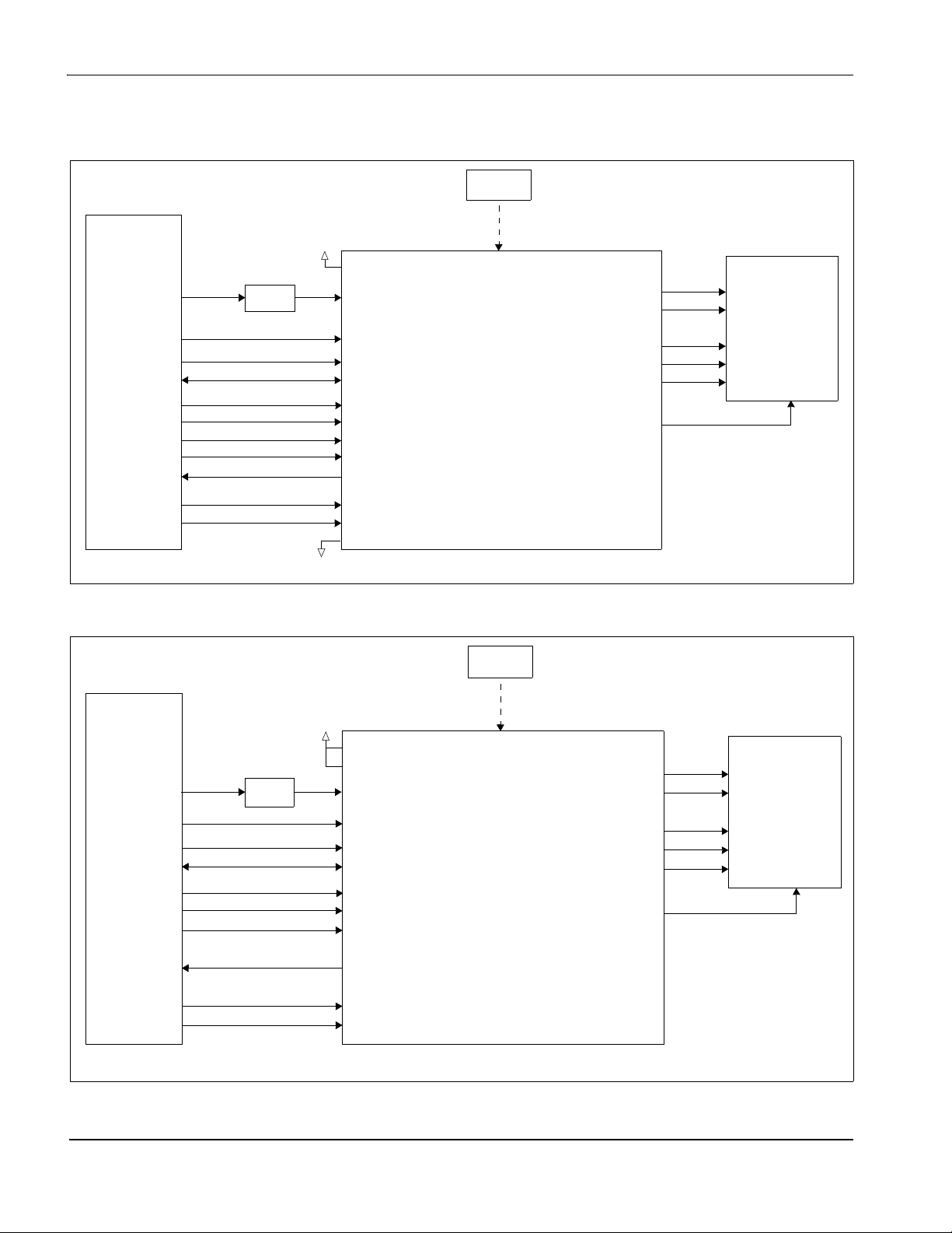
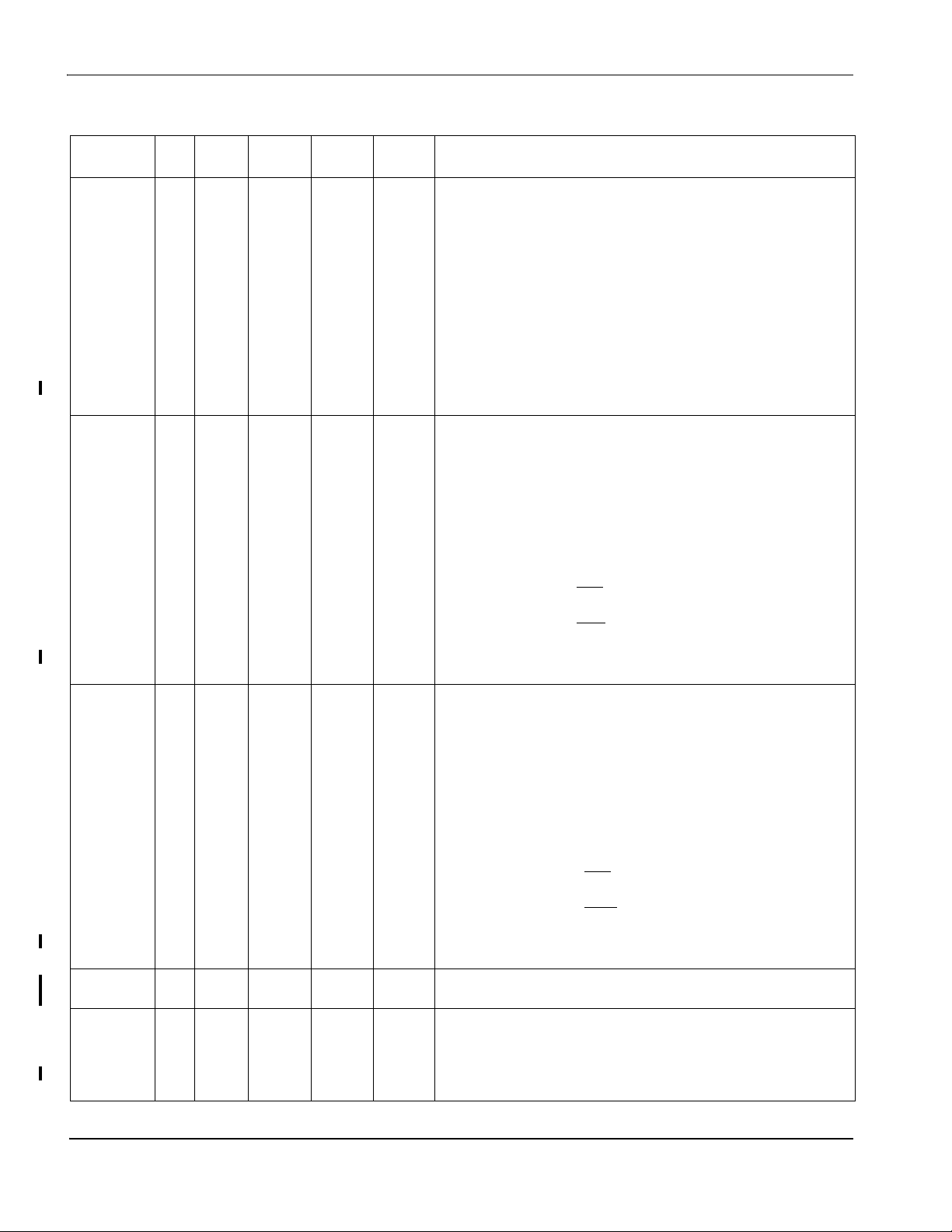
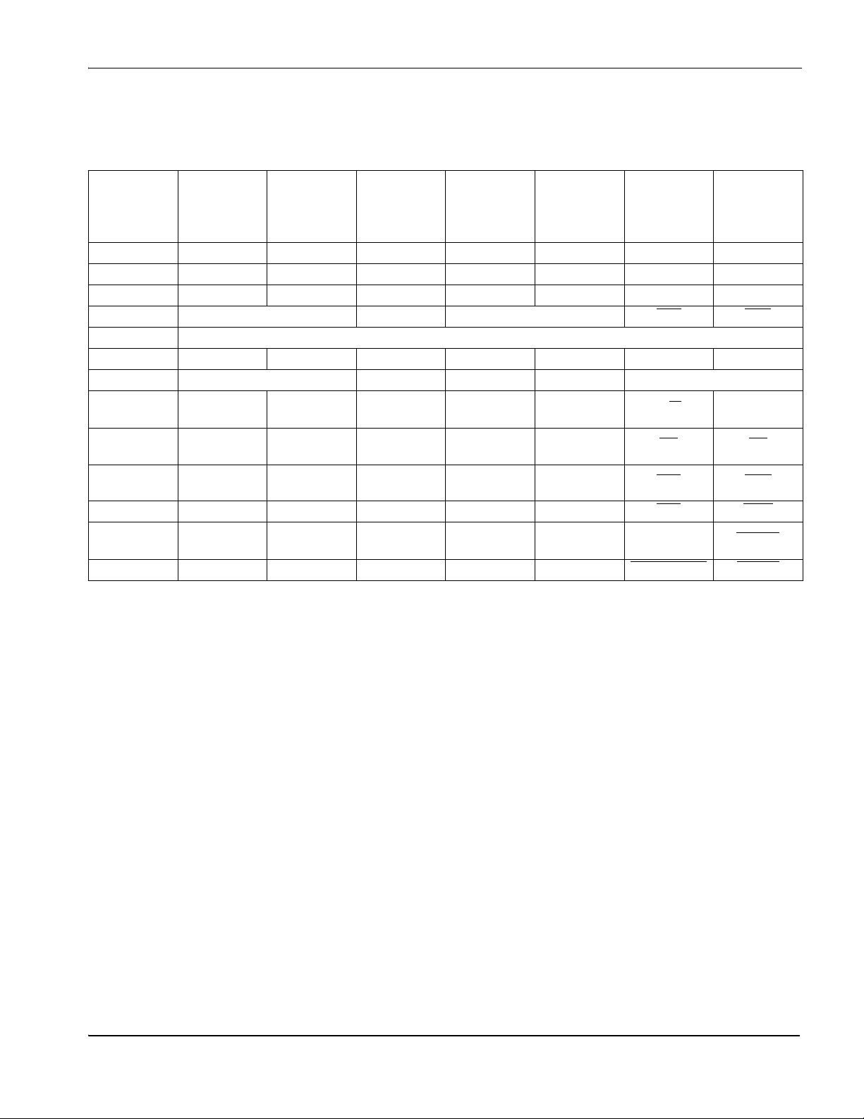
3 Typical System Implementation Diagrams
.
Oscillator
Generic #1
BUS
A[27:17]
CSn#
A[16:1]
D[15:0]
WE0#
WE1#
RD0#
RD1#
WAIT#
BUSCLK
RESET#
HIOVDD
Decoder
VSS
BS#
M/R#
CS#
AB[16:1]
DB[15:0]
WE0#
WE1#
RD#
RD/WR#
WAIT#
CLKI
RESET#
AB0
CLKI2
S1D13706
FPDAT[15:0]
FPFRAME
FPLINE
FPSHIFT
DRDY
GPO
D[15:0]
FPFRAME
FPLINE
FPSHIFT
MOD
16-bit
Single
LCD
Display
Bias Power
Generic #2
BUS
A[27:17]
CSn#
A[16:0]
D[15:0]
BHE#
WAIT#
BUSCLK
RESET#
WE#
RD#
Figure 3-1: Typical System Diagram (Generic #1 Bus)
.
Oscillator
VDD
Decoder
BS#
RD/WR#
M/R#
CS#
AB[16:0]
DB[15:0]
WE0#
WE1#
RD#
WAIT#
CLKI
RESET#
S1D13706
CLKI2
FPDAT[8:0]
FPFRAME
FPLINE
FPSHIFT
DRDY
GPO
D[8:0]
FPFRAME
FPLINE
FPSHIFT
DRDY
9-bit
TFT
Display
Bias Power
Figure 3-2: Typical System Diagram (Generic #2 Bus)
S1D13706 Hardware Functional Specification
X31B-A-001-09 Issue Date: 2004/02/09
Page 15
Epson Research and Development Page 15
Vancouver Design Center
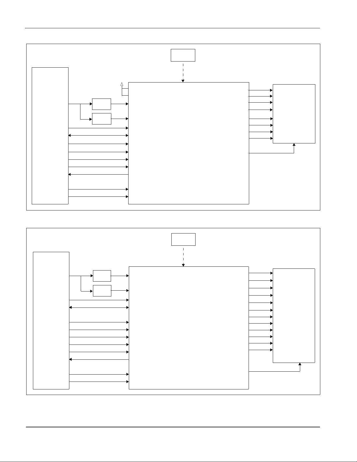
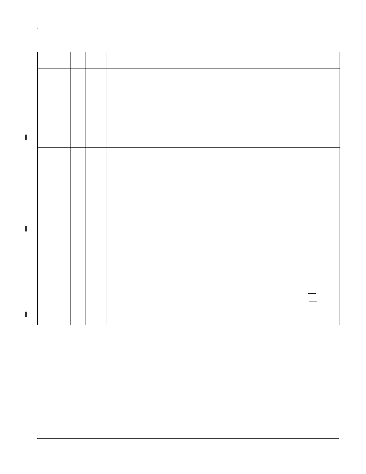
.
Oscillator
SH-4
BUS
A[25:17]
CSn#
A[16:1]
D[15:0]
WE0#
WE1#
BS#
RD/WR#
RD#
RDY#
CKIO
RESET#
Decoder
VSS
M/R#
CS#
AB[16:1]
DB[15:0]
WE0#
WE1#
BS#
RD/WR#
RD#
WAIT#
CLKI
RESET#
AB0
CLKI2
S1D13706
Figure 3-3: Typical System Diagram (Hitachi SH-4 Bus)
.
Oscillator
FPDAT15
FPDAT12
FPDAT[9:0]
FPFRAME
FPLINE
FPSHIFT
DRDY
GPO
D11
D10
D[9:0]
FPFRAME
FPLINE
FPSHIFT
DRDY
12-bit
TFT
Display
Bias Power
SH-3
BUS
A[25:17]
CSn#
A[16:1]
D[15:0]
WE0#
WE1#
BS#
RD/WR#
RD#
WAIT#
CKIO
RESET#
Decoder
VSS
M/R#
CS#
AB[16:1]
DB[15:0]
WE0#
WE1#
BS#
RD/WR#
RD#
WAIT#
CLKI
RESET#
AB0
CLKI2
S1D13706
Figure 3-4: Typical System Diagram (Hitachi SH-3 Bus)
FPDAT[17:0]
FPFRAME
FPLINE
FPSHIFT
DRDY
GPO
D[17:0]
FPFRAME
FPLINE
FPSHIFT
DRDY
18-bit
TFT
Display
Bias Power
Hardware Functional Specification S1D13706
Issue Date: 2004/02/09 X31B-A-001-09
Page 16
Page 16 Epson Research and Development
Vancouver Design Center
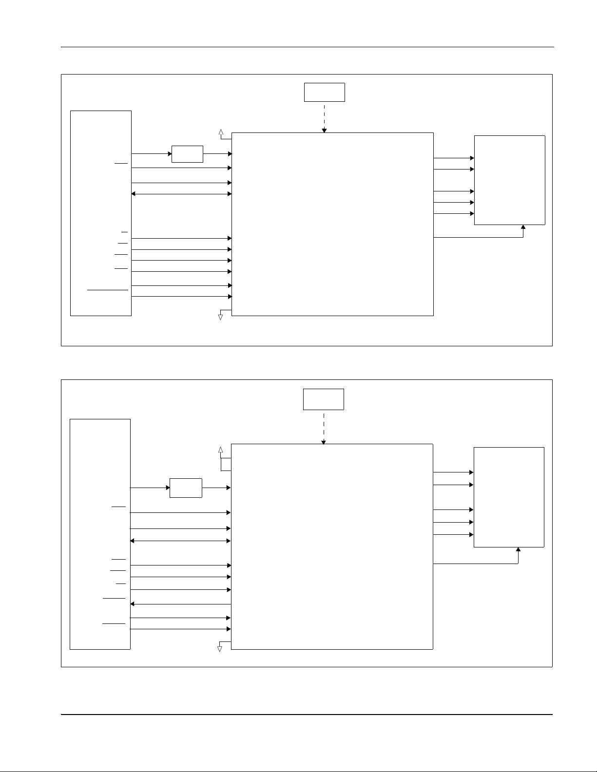
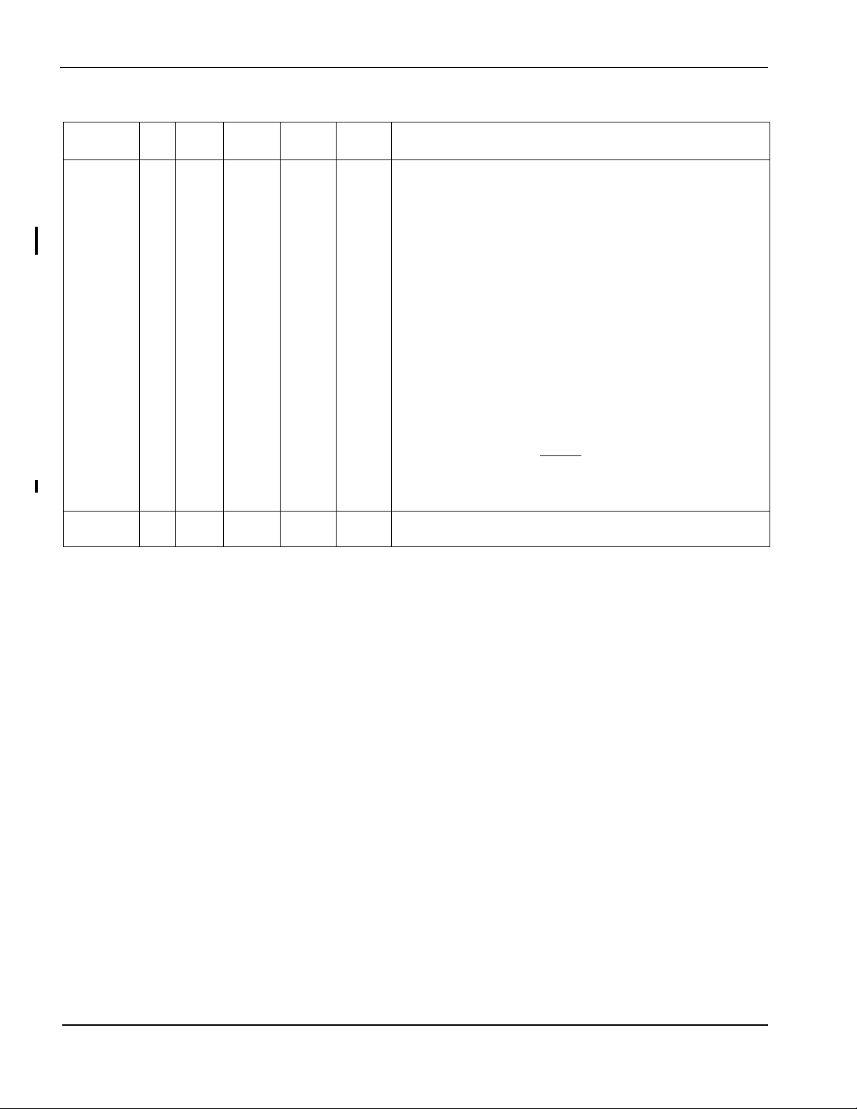
.
Oscillator
MC68K #1
BUS
A[23:17]
FC0, FC1
A[16:1]
D[15:0]
LDS#
UDS#
AS#
R/W#
DTACK#
HIOVDD
Decoder
Decoder
RD#
WE0#
M/R#
CS#
AB[16:1]
DB[15:0]
AB0
WE1#
BS#
RD/WR#
WAIT#
CLKI2
S1D13706
FPDAT[17:0]
FPFRAME
FPLINE
FPSHIFT
GPIO0
GPIO1
GPIO2
GPIO3
GPO
D[17:0]
SPS
LP
CLK
PS
CLS
REV
SPL
18-bit
HR-TFT
Display
Bias Power
RESET#
MC68K #2
BUS
A[31:17]
FC0, FC1
A[16:0]
D[31:16]
R/W#
DSACK1#
CLK
DS#
AS#
SIZ1
SIZ0
CLKI
RESET#
Figure 3-5: Typical System Diagram (MC68K # 1, Motorola 16-Bit 68000)
.
Oscillator
Decoder
Decoder
M/R#
CS#
AB[16:0]
DB[15:0]
WE1#
BS#
RD/WR#
RD#
WE0#
WAIT#
CLKI2
S1D13706
FPDAT[17:0]
FPFRAME
FPLINE
FPSHIFT
DRDY
GPIO0
GPIO1
GPIO2
GPIO3
GPIO4
GPIO5
GPIO6
D[17:0]
DY
LP
XSCL
GCP
XINH
YSCL
FR
FRS
RES
DD_P1
YSCLD
18-bit
D-TFD
Display
XSET (Bias Power)
CLK
RESET#
CLKI
RESET#
GPO
Figure 3-6: Typical System Diagram (MC68K #2, Motorola 32-Bit 68030)
S1D13706 Hardware Functional Specification
X31B-A-001-09 Issue Date: 2004/02/09
Page 17
Epson Research and Development Page 17
Vancouver Design Center
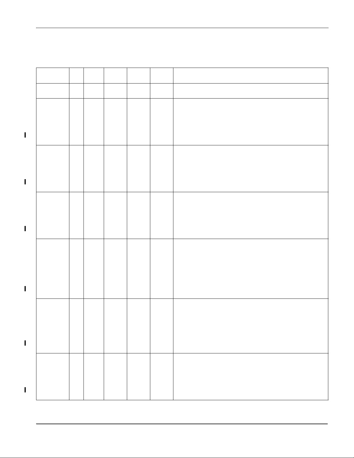
.
Oscillator
REDCAP2
BUS
A[21:17]
CSn
A[16:1]
D[15:0]
R/W
OE
EB1
EB0
CLK
RESET_OUT
Decoder
HIOVDD
VSS
BS#
M/R#
CS#
AB[16:1]
DB[15:0]
RD/WR#
RD#
WE0#
WE1#
CLKI
RESET#
AB0
CLKI2
S1D13706
FPDAT[7:4]
FPSHIFT
FPFRAME
FPLINE
DRDY
GPO
D[3:0]
FPSHIFT
FPFRAME
FPLINE
MOD
4-bit
Single
LCD
Display
Bias Power
*Note: CSn# can be any of CS0-CS4
Figure 3-7: Typical System Diagram (Motorola REDCAP2 Bus)
MC68EZ328/
MC68VZ328
DragonBall
BUS
A[25:17]
CS
A[16:1]
D[15:0]
LWE
UWE
OE
DTACK
CLKO
RESET
X
Decoder
HIOVDD
VSS
BS#
RD/WR#
M/R#
CS#
AB[16:1]
DB[15:0]
WE0#
WE1#
RD#
WAIT#
CLKI
RESET#
AB0
.
Oscillator
CLKI2
S1D13706
FPDAT[7:0]
FPSHIFT
FPFRAME
FPLINE
DRDY
GPO
D[7:0]
FPSHIFT
FPFRAME
FPLINE
MOD
8-bit
Single
LCD
Display
Bias Power
Figure 3-8: Typical System Diagram (Motorola MC68EZ328/MC68VZ328 “DragonBall” Bus)
Hardware Functional Specification S1D13706
Issue Date: 2004/02/09 X31B-A-001-09
Page 18
Page 18 Epson Research and Development
Vancouver Design Center
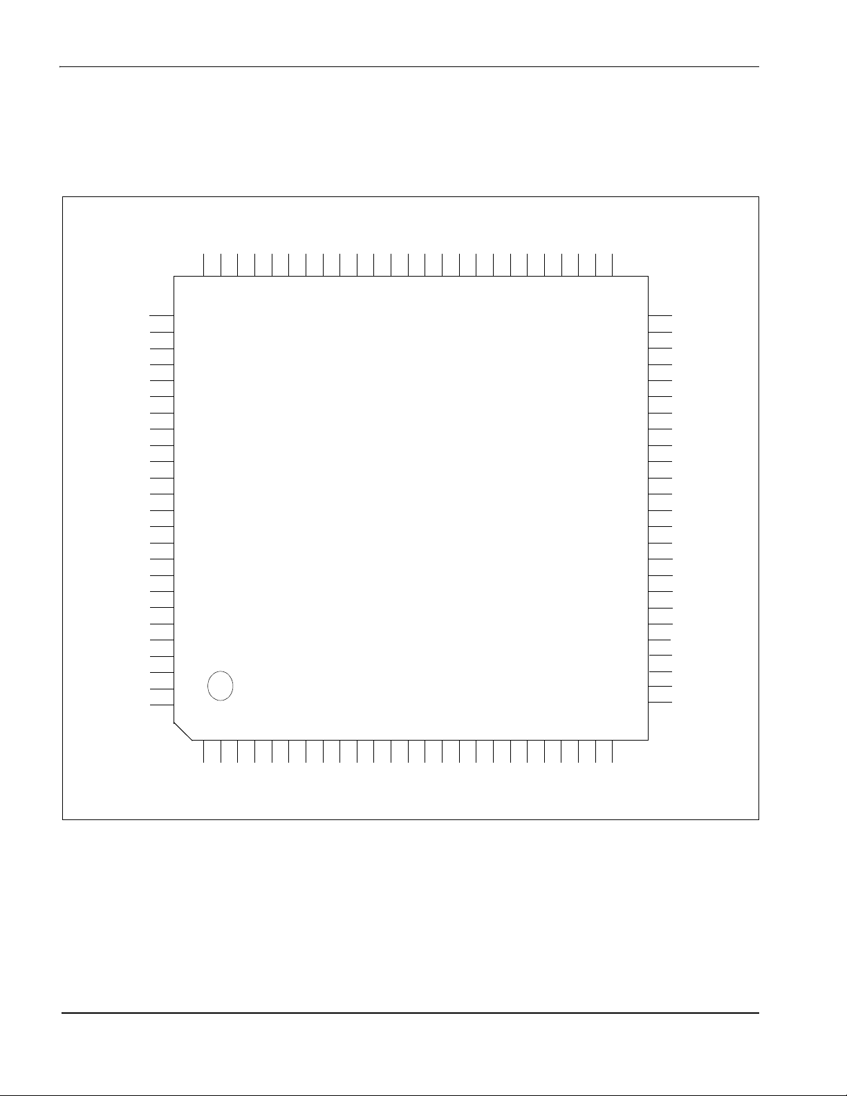
4 Pins
4.1 Pinout Diagram - TQFP15 - 100pin
75747372717069686766656463626160595857565554535251
VSS
FPDAT17
FPDAT16
FPDAT15
FPDAT14
FPDAT13
FPDAT12
FPDAT11
FPDAT10
FPDAT9
FPDAT8
FPDAT7
NIOVDD
VSS
FPDAT6
FPDAT5
FPDAT4
FPDAT3
FPDAT2
FPDAT1
FPDAT0
FPSHIFT
FPLINE
FPFRAME
COREVDD
76
77
78
79
80
81
82
83
84
85
86
87
88
89
90
91
92
93
94
95
96
97
98
99
100
NIOVDD
CLKI2
CNF7
CNF6
CNF5
CNF4
CNF3
CNF2
CNF1
CNF0
TESTEN
AB16
AB15
AB14
AB13
AB12
AB11
AB10
AB9
AB8
AB7
AB6
AB5
COREVDD
AB4
VSS
AB3
AB2
AB1
AB0
CS#
50
VSS
DRDY
GPO
GPIO0
GPIO1
GPIO2
GPIO3
GPIO4
GPIO5
GPIO6
VSS
DB0
DB1
DB2
DB3
DB4
DB5
DB6
DB7
DB8
49
48
47
46
45
44
43
42
41
40
39
38
37
36
35
34
33
32
31
30
29
28
27
26
NIOVDD
CVOUT
DB10
PWMOUT
NIOVDD
HIOVDD
VSS
DB9
S1D13706
RD/WR#
RESET#
WE1#
BS#
RD#
WE0#
M/R#
VSS
HIOVDD
WAIT#
DB15
DB14
DB13
DB12
CLKI
DB11
1
2
3
4
5
6
7
101112131415161718192021222324
8
9
25
Figure 4-1: Pinout Diagram - TQFP15 - 100pin (S1D13706F00A)
Note
Package type: 100 pin surface mount TQFP15
S1D13706 Hardware Functional Specification
X31B-A-001-09 Issue Date: 2004/02/09
Page 19
Epson Research and Development Page 19
Vancouver Design Center
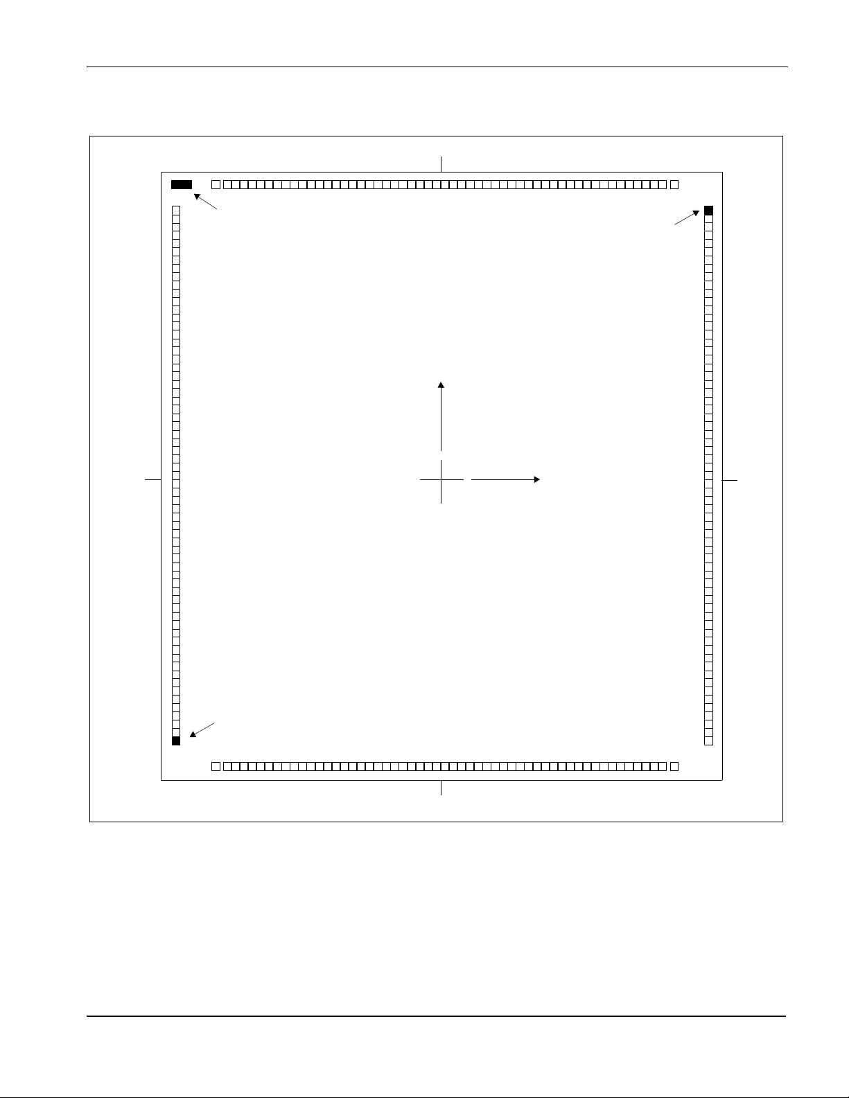
4.2 Pinout Diagram - Die Form
120125130135140145150155160165170
175
DIE No. X5534D
180
Unusable Pad
115
185
190
195
200
205
210
215
220
225
230
Y
(0,0)
110
105
100
95
90
X
85
80
75
70
65
235
Unusable Pad
15 10 403530252015
555045
60
Figure 4-2: Pinout Diagram - Die Form (S1D13706D00A)
Chip Size: 5.88 x 6.55 mm
PAD size: 68 x 68
Hardware Functional Specification S1D13706
Issue Date: 2004/02/09 X31B-A-001-09
µm
Page 20
Page 20 Epson Research and Development
Vancouver Design Center
Table 4-1: Pinout Assignments - Die Form (S1D13706D00A)
Pin No. Pad No. Pin Name X (µm) Y (µm) Pin No. Pad No. Pin Name X (µm) Y (µm)
1 1 LVDD -2331 -3149 51 119 LVDD 2813 2667
2 3 AB3 -2100 -3149 52 122 FPFRAME 2100 3149
3 5 AB2 -1932 -3149 53 124 FPLINE 1932 3149
4 8 AB1 -1680 -3149 54 127 FPSHIFT 1680 3149
5 10 AB0 -1512 -3149 55 129 FPDAT0 1512 3149
6 12 CS# -1344 -3149 56 131 FPDAT1 1344 3149
7 15 M/R# -1092 -3149 57 134 FPDAT2 1092 3149
8 17 BS# -924 -3149 58 136 FPDAT3 924 3149
9 20 RD# -672 -3149 59 139 FPDAT4 672 3149
10 22 WE0# -504 -3149 60 141 FPDAT5 504 3149
11 24 WE1# -336 -3149 61 143 FPDAT6 336 3149
12 27 RD/WR# -84 -3149 62 146 VSS 84 3149
13 29 RESET# 84 -3149 63 148 HVDD -84 3149
14 31 VSS 252 -3149 64 150 FPDAT7 -252 3149
15 34 CLKI 504 -3149 65 153 FPDAT8 -504 3149
16 36 HVDD 672 -3149 66 155 FPDAT9 -672 3149
17 39 WAIT# 924 -3149 67 158 FPDAT10 -924 3149
18 41 DB15 1092 -3149 68 160 FPDAT11 -1092 3149
19 43 DB14 1260 -3149 69 162 FPDAT12 -1260 3149
20 46 DB13 1512 -3149 70 165 FPDAT13 -1512 3149
21 48 DB12 1680 -3149 71 167 FPDAT14 -1680 3149
22 50 DB11 1848 -3149 72 169 FPDAT15 -1848 3149
23 53 DB10 2100 -3149 73 172 FPDAT16 -2100 3149
24 55 DB9 2331 -3149 74 174 FPDAT17 -2331 3149
25 58 VSS 2813 -2478 75 177 VSS -2813 2478
26 60 HVDD 2813 -2310 76 179 HVDD -2813 2310
27 62 DB8 2813 -2142 77 181 CLKI2 -2813 2142
28 65 DB7 2813 -1890 78 184 CNF7 -2813 1890
29 67 DB6 2813 -1722 79 186 CNF6 -2813 1722
30 70 DB5 2813 -1470 80 189 CNF5 -2813 1470
31 72 DB4 2813 -1302 81 191 CNF4 -2813 1302
32 74 DB3 2813 -1134 82 193 CNF3 -2813 1134
33 77 DB2 2813 -882 83 196 CNF2 -2813 882
34 79 DB1 2813 -714 84 198 CNF1 -2813 714
35 81 DB0 2813 -546 85 200 CNF0 -2813 546
36 84 VSS 2813 -294 86 203 TESTEN -2813 294
37 86 HVDD 2813 -126 87 205 AB16 -2813 126
38 89 PWMOUT 2813 126 88 208 AB15 -2813 -126
39 91 GPIO6 2813 294 89 210 AB14 -2813 -294
40 93 GPIO5 2813 462 90 212 AB13 -2813 -462
41 96 GPIO4 2813 714 91 215 AB12 -2813 -714
42 98 GPIO3 2813 882 92 217 AB11 -2813 -882
43 100 GPIO2 2813 1050 93 219 AB10 -2813 -1050
44 103 GPIO1 2813 1302 94 222 AB9 -2813 -1302
45 105 GPIO0 2813 1470 95 224 AB8 -2813 -1470
46 108 CVOUT 2813 1722 96 227 AB7 -2813 -1722
47 110 GPO 2813 1890 97 229 AB6 -2813 -1890
48 112 DRDY 2813 2058 98 231 AB5 -2813 -2058
49 115 HVDD 2813 2310 99 234 AB4 -2813 -2310
50 117 VSS 2813 2478 100 236 VSS -2813 -2478
S1D13706 Hardware Functional Specification
X31B-A-001-09 Issue Date: 2004/02/09
Page 21
Epson Research and Development Page 21
Vancouver Design Center
4.3 Pin Descriptions
Key:
I = Input
O=Output
IO = Bi-Directional (Input/Output)
P=Power pin
LIS = LVTTL
LI = LVTTL input
LB2A = LVTTL IO buffer (6mA/-6mA@3.3V)
LB3P = Low noise LVTTL IO buffer (12mA/-12mA@3.3V)
LO3 = Low noise LVTTL Output buffer (12mA/-12mA@3.3V)
LB3M = Low noise LVTTL IO buffer with input mask (12mA/-12mA@3.3V)
T1 = Test mode control input with pull-down resistor (typical value of 50Ω at 3.3V)
Hi-Z = High Impedance
a
Schmitt input
a
LVTTL is Low Voltage TTL (see Section 5, “D.C. Characteristics” on page 31).
4.3.1 Host Interface
Table 4-2: Host Interface Pin Descriptions
Pin Name Type Pin # Cell
AB0 I 5 LIS HIOVDD 0
AB[16:1] I
87-99,
2-4
LI HIOVDD 0 System address bus bits 16-1.
IO
Vol tage
RESET#
State
Description
This input pin has multiple functions.
• For Generic #1, this pin is not used and should be connected
to VSS.
• For Generic #2, this pin inputs system address bit 0 (A0).
• For SH-3/SH-4, this pin is not used and should be connected
to VSS.
• For MC68K #1, this pin inputs the lower data strobe (LDS#).
• For MC68K #2, this pin inputs system address bit 0 (A0).
• For REDCAP2, this pin is not used and should be connected
to VSS.
• For DragonBall, this pin is not used and should be connected
to VSS.
See Table 4-8: “Host Bus Interface Pin Mapping,” on page 29 for
summary.
Hardware Functional Specification S1D13706
Issue Date: 2004/02/09 X31B-A-001-09
Page 22
Page 22 Epson Research and Development
Vancouver Design Center
Table 4-2: Host Interface Pin Descriptions
IO
Pin Name Type Pin # Cell
DB[15:0] IO
18-24,
27-35
LB2A HIOVDD Hi-Z
Volta ge
WE0# I 10 LIS HIOVDD 1
WE1# I 11 LIS HIOVDD 1
CS# I 6 LI HIOVDD 1
M/R# I 7 LIS HIOVDD 0
RESET#
State
Input data from the system data bus.
• For Generic #1, these pins are connected to D[15:0].
• For Generic #2, these pins are connected to D[15:0].
• For SH-3/SH-4, these pins are connected to D[15:0].
• For MC68K #1, these pins are connected to D[15:0].
• For MC68K #2, these pins are connected to D[31:16] for a 32bit device (e.g. MC68030) or D[15:0] for a 16-bit device (e.g.
MC68340).
• For REDCAP2, these pins are connected to D[15:0].
• For DragonBall, these pins are connected to D[15:0].
See Table 4-8: “Host Bus Interface Pin Mapping,” on page 29 for
summary.
This input pin has multiple functions.
• For Generic #1, this pin inputs the write enable signal for the
lower data byte (WE0#).
• For Generic #2, this pin inputs the write enable signal (WE#)
• For SH-3/SH-4, this pin inputs the write enable signal for data
byte 0 (WE0#).
• For MC68K #1, this pin must be tied to HIO V
• For MC68K #2, this pin inputs the bus size bit 0 (SIZ0).
• For REDCAP2, this pin inputs the byte enable signal for the
D[7:0] data byte (EB1).
• For DragonBall, this pin inputs the byte enable signal for the
D[7:0] data byte (LWE
See Table 4-8: “Host Bus Interface Pin Mapping,” on page 29 for
summary.
This input pin has multiple functions.
• For Generic #1, this pin inputs the write enable signal for the
upper data byte (WE1#).
• For Generic #2, this pin inputs the byte enable signal for the
high data byte (BHE#).
• For SH-3/SH-4, this pin inputs the write enable signal for data
byte 1 (WE1#).
• For MC68K #1, this pin inputs the upper data strobe (UDS#).
• For MC68K #2, this pin inputs the data strobe (DS#).
• For REDCAP2, this pin inputs the byte enable signal for the
D[15:8] data byte (EB0
• For DragonBall, this pin inputs the byte enable signal for the
D[15:8] data byte (UWE
See Table 4-8: “Host Bus Interface Pin Mapping,” on page 29 for
summary.
Chip select input. See Table 4-8: “Host Bus Interface Pin Mapping,”
on page 29 for summary.
This input pin is used to select between the display buffer and
register address spaces of the S1D13706. M/R# is set high to
access the display buffer and low to access the registers. See
Table 4-8: “Host Bus Interface Pin Mapping,” on page 29 for
summary.
Description
DD
).
).
).
S1D13706 Hardware Functional Specification
X31B-A-001-09 Issue Date: 2004/02/09
Page 23
Epson Research and Development Page 23
Vancouver Design Center
Table 4-2: Host Interface Pin Descriptions
IO
Pin Name Type Pin # Cell
Vol tage
RESET#
BS# I 8 LIS HIOVDD 1
RD/WR# I 12 LIS HIOVDD 1
RD# I 9 LIS HIOVDD 1
State
This input pin has multiple functions.
• For Generic #1, this pin must be tied to HIO VDD.
• For Generic #2, this pin must be tied to HIO VDD.
• For SH-3/SH-4, this pin inputs the bus start signal (BS#).
• For MC68K #1, this pin inputs the address strobe (AS#).
• For MC68K #2, this pin inputs the address strobe (AS#).
• For REDCAP2, this pin must be tied to HIO V
• For DragonBall, this pin must be tied to HIO VDD.
See Table 4-8: “Host Bus Interface Pin Mapping,” on page 29 for
summary.
This input pin has multiple functions.
• For Generic #1, this pin inputs the read command for the
upper data byte (RD1#).
• For Generic #2, this pin must be tied to HIO V
• For SH-3/SH-4, this pin inputs the RD/WR# signal. The
S1D13706 needs this signal for early decode of the bus cycle.
• For MC68K #1, this pin inputs the R/W# signal.
• For MC68K #2, this pin inputs the R/W# signal.
• For REDCAP2, this pin inputs the R/W
• For DragonBall, this pin must be tied to HIO VDD.
See Table 4-8: “Host Bus Interface Pin Mapping,” on page 29 for
summary.
This input pin has multiple functions.
• For Generic #1, this pin inputs the read command for the
lower data byte (RD0#).
• For Generic #2, this pin inputs the read command (RD#).
• For SH-3/SH-4, this pin inputs the read signal (RD#).
• For MC68K #1, this pin must be tied to HIO VDD.
• For MC68K #2, this pin inputs the bus size bit 1 (SIZ1).
• For REDCAP2, this pin inputs the output enable (OE).
• For DragonBall, this pin inputs the output enable (OE
See Table 4-8: “Host Bus Interface Pin Mapping,” on page 29 for
summary.
Description
signal.
DD
DD
.
.
).
Hardware Functional Specification S1D13706
Issue Date: 2004/02/09 X31B-A-001-09
Page 24
Page 24 Epson Research and Development
Vancouver Design Center
Table 4-2: Host Interface Pin Descriptions
IO
Pin Name Type Pin # Cell
Volta ge
RESET#
WAIT# O 17 LB2A HIOVDD Hi-Z
RESET# I 13 LIS HIOVDD 0
State
During a data transfer, this output pin is driven active to force the
system to insert wait states. It is driven inactive to indicate the
completion of a data transfer. WAIT# is released to the high
impedance state after the data transfer is complete. Its active
polarity is configurable. See Table 4-7: “Summary of PowerOn/Reset Options,” on page 28.
• For Generic #1, this pin outputs the wait signal (WAIT#).
• For Generic #2, this pin outputs the wait signal (WAIT#).
• For SH-3 mode, this pin outputs the wait request signal
(WAIT#).
• For SH-4 mode, this pin outputs the device ready signal
(RDY#).
• For MC68K #1, this pin outputs the data transfer acknowledge
signal (DTACK#).
• For MC68K #2, this pin outputs the data transfer and size
acknowledge bit 1 (DSACK1#).
• For REDCAP2, this pin is unused (Hi-Z).
• For DragonBall, this pin outputs the data transfer
acknowledge signal (DTACK
See Table 4-8: “Host Bus Interface Pin Mapping,” on page 29 for
summary.
Active low input to set all internal registers to the default state and
to force all signals to their inactive states.
Description
).
S1D13706 Hardware Functional Specification
X31B-A-001-09 Issue Date: 2004/02/09
Page 25
Epson Research and Development Page 25
Vancouver Design Center
4.3.2 LCD Interface
Table 4-3: LCD Interface Pin Descriptions
IO
Pin Name Type Pin # Cell
FPDAT[17:0] O
FPFRAME O 52 LB3P NIOVDD 0
FPLINE O 53 LB3P NIOVDD 0
FPSHIFT O 54 LB3P NIOVDD 0
DRDY O 48 LO3 NIOVDD 0
GPIO0 IO 45 LB3M NIOVDD 0
GPIO1 IO 44 LB3M NIOVDD 0
74-64,
61-55
LB3P NIOVDD 0 Panel Data bits 17-0.
Volta ge
RESET#
State
This output pin has multiple functions.
•Frame Pulse
• SPS for Sharp HR-TFT
• DY for Epson D-TFD
See Table 4-9: “LCD Interface Pin Mapping,” on page 30 for
summary.
This output pin has multiple functions.
•Line Pulse
• LP for Sharp HR-TFT
• LP for Epson D-TFD
See Table 4-9: “LCD Interface Pin Mapping,” on page 30 for
summary.
This output pin has multiple functions.
• Shift Clock
• CLK for Sharp HR-TFT
• XSCL for Epson D-TFD
See Table 4-9: “LCD Interface Pin Mapping,” on page 30 for
summary.
This output pin has multiple functions.
• Display enable (DRDY) for TFT panels
• 2nd shift clock (FPSHIFT2) for passive LCD with Format 1
interface
• GCP for Epson D-TFD
• LCD backplane bias signal (MOD) for all other LCD panels
See Table 4-9: “LCD Interface Pin Mapping,” on page 30 for
summary.
This pin has multiple functions.
• PS for Sharp HR-TFT
• XINH for Epson D-TFD
• General purpose IO pin 0 (GPIO0)
• Hardware Video Invert
See Table 4-9: “LCD Interface Pin Mapping,” on page 30 for
summary.
This pin has multiple functions.
• CLS for Sharp HR-TFT
• YSCL for Epson D-TFD
• General purpose IO pin 1 (GPIO1)
See Table 4-9: “LCD Interface Pin Mapping,” on page 30 for
summary.
Description
Hardware Functional Specification S1D13706
Issue Date: 2004/02/09 X31B-A-001-09
Page 26

Page 26 Epson Research and Development
Vancouver Design Center
Table 4-3: LCD Interface Pin Descriptions
IO
Pin Name Type Pin # Cell
Vol tage
RESET#
State
GPIO2 IO 43 LB3M NIOVDD 0
GPIO3 IO 42 LB3M NIOVDD 0
GPIO4 IO 41 LB3M NIOVDD 0
GPIO5 IO 40 LB3M NIOVDD 0
GPIO6 IO 39 LB3M NIOVDD 0
PWMOUT O 38 LB3P NIOVDD 0
CVOUT O 46 LB3P NIOVDD 0
This pin has multiple functions.
• REV for Sharp HR-TFT
• FR for Epson D-TFD
• General purpose IO pin 2 (GPIO2)
See Table 4-9: “LCD Interface Pin Mapping,” on page 30 for
summary.
This pin has multiple functions.
• SPL for Sharp HR-TFT
• FRS for Epson D-TFD
• General purpose IO pin 3 (GPIO3)
See Table 4-9: “LCD Interface Pin Mapping,” on page 30 for
summary.
This pin has multiple functions.
• RES for Epson D-TFD
• General purpose IO pin 4 (GPIO4)
See Table 4-9: “LCD Interface Pin Mapping,” on page 30 for
summary.
This pin has multiple functions.
• DD_P1 for Epson D-TFD
• General purpose IO pin 5 (GPIO5)
See Table 4-9: “LCD Interface Pin Mapping,” on page 30 for
summary.
This pin has multiple functions.
• YSCLD for Epson D-TFD
• General purpose IO pin 6 (GPIO6)
See Table 4-9: “LCD Interface Pin Mapping,” on page 30 for
summary.
This output pin has multiple functions.
• PWM Clock output
• General purpose output
This output pin has multiple functions.
• CV Pulse Output
• General purpose output
Description
S1D13706 Hardware Functional Specification
X31B-A-001-09 Issue Date: 2004/02/09
Page 27
Epson Research and Development Page 27
Vancouver Design Center
4.3.3 Clock Input
Table 4-4: Clock Input Pin Descriptions
IO
Pin Name Type Pin # Cell
CLKI I 15 LI NIOVDD —
CLKI2 I 77 LI NIOVDD — Typically used as input clock source for pixel clock
Vol tage
RESET#
State
Typically used as input clock source for bus clock and memory
clock
Description
4.3.4 Miscellaneous
Table 4-5: Miscellaneous Pin Descriptions
IO
Pin Name Type Pin # Cell
CNF[7:0] I 78-85 LI NIOVDD —
GPO O 47 LO3 NIOVDD 0
TESTEN I 86 T1 NIOVDD 0
Vol tage
RESET#
State
These inputs are used to configure the S1D13706 - see Table 4-7:
“Summary of Power-On/Reset Options,” on page 28.
Note: These pins are used for configuration of the S1D13706
and must be connected directly to IO V
General Purpose Output (possibly used for controlling the LCD
power). It may also be used for the MOD control signal of the Sharp
HR-TFT panel.
Test Enable input used for production test only (has type 1 pull-
down resistor with a typical value of 50Ω at 3.3V).
Description
or VSS.
DD
4.3.5 Power And Ground
Table 4-6: Power And Ground Pin Descriptions
IO
Pin Name Type Pin # Cell
HIOVDD P 16, 26 P — —
NIOVDD P
COREVDD P 1, 51 P — — 2 Core V
VSS P
37, 49,
63, 76
14, 25,
36, 50,
62, 75,
100
Vol tage
P——
P——7 V
RESET#
State
IO V
Section 4.3.1, “Host Interface” on page 21.
IO V
described in Section 4.3.2, “LCD Interface” on page 25, Section
4.3.3, “Clock Input” on page 27, and Section 4.3.4, “Miscellaneous”
on page 27.
SS
Description
pins associated with the host interface pins as described in
DD
pins associated with the non-host interface pins as
DD
pins.
DD.
pins.
Hardware Functional Specification S1D13706
Issue Date: 2004/02/09 X31B-A-001-09
Page 28
Page 28 Epson Research and Development
Vancouver Design Center
4.4 Summary of Configuration Options
These pins are used for configuration of the S1D13706 and must be connected directly to
NIOV
state at any other time has no effect.
S1D13706
Configuration
Input
Select host bus interface as follows:
CNF4,CNF[2:0]
or VSS. The state of CNF[6:0] is latched on the rising edge of RESET#. Changing
DD
Table 4-7: Summary of Power-On/Reset Options
Power-On/Reset State
1 (connected to NIOV
CNF4 CNF2 CNF1 CNF0 Host Bus
1000 SH-4/SH-3 interface, Big Endian
0000 SH-4/SH-3 interface, Little Endian
1001 MC68K #1, Big Endian
0001 Reserved
1010 MC68K #2, Big Endian
0010 Reserved
1011 Generic #1, Big Endian
0011 Generic #1, Little Endian
1100 Reserved
0100 Generic #2, Little Endian
1101 REDCAP2, Big Endian
0101 Reserved
1110 DragonBall (MC68EZ328/MC68VZ328), Big Endian
0110 Reserved
X111 Reserved
) 0 (Connected to VSS)
DD
Note: The host bus interface is 16-bit only.
CNF3 Configure GPIO pins as inputs at power-on
CNF5 WAIT# is active high WAIT# is active low
CLKI to BCLK divide select:
CNF7 CNF6 CLKI to BCLK Divide Ratio
CNF[7:6]
00 1 : 1
01 2 : 1
10 3 : 1
11 4 : 1
Configure GPIO pins as outputs at power-on (for use
by HR-TFT/D-TFD when selected)
S1D13706 Hardware Functional Specification
X31B-A-001-09 Issue Date: 2004/02/09
Page 29
Epson Research and Development Page 29
Vancouver Design Center
4.5 Host Bus Interface Pin Mapping
Table 4-8: Host Bus Interface Pin Mapping
Motorola
S1D13706
Pin Name
Generic #1 Generic #2
Hitachi
SH-3 /SH-4
Motorola
MC68K #1
Motorola
MC68K #2
Motorola
REDCAP2
AB[16:1] A[16:1] A[16:1] A[16:1] A[16:1] A[16:1] A[16:1] A[16:1]
AB0 A0
1
A0 A0
DB[15:0] D[15:0] D[15:0] D[15:0] D[15:0] D[15:0]
1
LDS# A0 A0
2
1
D[15:0] D[15:0]
CS# External Decode CSn# External Decode CSn
M/R# External Decode
CLKI BUSCLK BUSCLK CKIO CLK CLK CLK CLKO
BS# Connected to V
RD/WR# RD1#
DD
Connected to
V
DD
RD# RD0# RD# RD#
WE0# WE0# WE# WE0#
BS# AS# AS# Connected to V
RD/WR# R/W# R/W# R/W
Connected to
V
DD
Connected to
V
DD
SIZ1 OE OE
SIZ0 EB1 LWE
WE1# WE1# BHE# WE1# UDS# DS# EB0 UWE
WAIT# WAIT# WAIT#
WAIT#/
RDY#
DTACK# DSACK1# N/A DTACK
RESET# RESET# RESET# RESET# RESET# RESET# RESET_OUT RESET
MC68EZ328/
MC68VZ328
DragonBall
1
A0
CSX
DD
Connected to
V
DD
Note
1
A0 for these busses is not used internally by the S1D13706 and should be connected to VSS.
2
If the target MC68K bus is 32-bit, then these signals should be connected to D[31:16].
Hardware Functional Specification S1D13706
Issue Date: 2004/02/09 X31B-A-001-09
Page 30
Page 30 Epson Research and Development
Vancouver Design Center
4.6 LCD Interface Pin Mapping
Table 4-9: LCD Interface Pin Mapping
Monochrome Passive
Panel
Pin Name
FPFRAME FPFRAME SPS DY
FPLINE FPLINE LP LP
FPSHIFT FPSHIFT DCLK XSCL
DRDY MOD FPSHIFT2 MOD DRDY
FPDAT0
FPDAT1
FPDAT2
FPDAT3
FPDAT4 D0 D4 D0 (R2)
FPDAT5 D1 D5 D1 (B1)
FPDAT6 D2 D6 D2 (G1)
FPDAT7 D3 D7 D3 (R1)
FPDAT8
FPDAT9
FPDAT10
FPDAT11
FPDAT12
FPDAT13
FPDAT14
FPDAT15
FPDAT16
FPDAT17
GPIO0 GPIO0 GPIO0 GPIO0 GPIO0 GPIO0 GPIO0 GPIO0 GPIO0 GPIO0 PS XINH
GPIO1 GPIO1 GPIO1 GPIO1 GPIO1 GPIO1 GPIO1 GPIO1 GPIO1 GPIO1 CLS YSCL
GPIO2 GPIO2 GPIO2 GPIO2 GPIO2 GPIO2 GPIO2 GPIO2 GPIO2 GPIO2 REV FR
GPIO3 GPIO3 GPIO3 GPIO3 GPIO3 GPIO3 GPIO3 GPIO3 GPIO3 GPIO3 SPL FRS
GPIO4 GPIO4 GPIO4 GPIO4 GPIO4 GPIO4 GPIO4 GPIO4 GPIO4 GPIO4
GPIO5 GPIO5 GPIO5 GPIO5 GPIO5 GPIO5 GPIO5 GPIO5 GPIO5 GPIO5
GPIO6 GPIO6 GPIO6 GPIO6 GPIO6 GPIO6 GPIO6 GPIO6 GPIO6 GPIO6
GPO GPO (General Purpose Output) MOD
CVOUT CVOUT
PWMOUT PWMOUT
Single
4-bit 8-bit 9-bit 12-bit 18-bit 18-bit 18-bit
driven 0 D0 driven 0 D0 (B5)2D0 (G3)2D0 (R6)
driven 0 D1 driven 0 D1 (R5)2D1 (R3)2D1 (G5)
driven 0 D2 driven 0 D2 (G4)2D2 (B2)2D2 (B4)
driven 0 D3 driven 0 D3 (B3)2D3 (G2)2D3 (R4)
driven 0 driven 0 driven 0 driven 0 driven 0 D4 (G3)
driven 0 driven 0 driven 0 driven 0 driven 0 D5 (B2)2driven 0R0R2R2R2
driven 0 driven 0 driven 0 driven 0 driven 0 D6 (R2)2driven 0 driven 0R1R1R1
driven 0 driven 0 driven 0 driven 0 driven 0 D7 (G1)2driven 0 driven 0R0R0R0
driven 0 driven 0 driven 0 driven 0 driven 0 D12 (R3)2driven 0G0G2G2G2
driven 0 driven 0 driven 0 driven 0 driven 0 D13 (G2)2driven 0 driven 0G1G1G1
driven 0 driven 0 driven 0 driven 0 driven 0 D14 (B1)2driven 0 driven 0G0G0G0
driven 0 driven 0 driven 0 driven 0 driven 0 D15 (R1)2driven 0B0B2B2B2
driven 0 driven 0 driven 0 driven 0 driven 0 driven 0 driven 0 driven 0B1B1B1
driven 0 driven 0 driven 0 driven 0 driven 0 driven 0 driven 0 driven 0B0B0B0
4-bit
Color Passive Panel Color TFT Panel
Single
Format 1
8-bit
2
D4 (R3)
2
D5 (G2)
2
D6 (B1)2D6 (G1)2D10 (G4)
2
D7 (R1)
Format 2
8-bit
2
D4 (R2)2D8 (B5)
2
D5 (B1)2D9 (R5)
2
D7 (R1)2D11 (B3)
16-Bit
2
R2 R3 R5 R5 R5
2
R1 R2 R4 R4 R4
2
R0 R1 R3 R3 R3
2
G2 G3 G5 G5 G5
2
G1 G2 G4 G4 G4
2
G0 G1 G3 G3 G3
2
B2 B3 B5 B5 B5
2
B1 B2 B4 B4 B4
2
B0 B1 B3 B3 B3
Others
Sharp HR-
TFT
no connect GCP
GPIO4
(output only)
GPIO5
(output only)
GPIO6
(output only)
Epson
1
D-TFD
RES
DD_P1
YSCLD
3
GPO
1
Note
1
GPIO pins must be configured as outputs (CNF3 = 0 at RESET#) when the HR-TFT or
D-TFD interface is selected.
2
These pin mappings use signal names commonly used for each panel type, however
signal names may differ between panel manufacturers. The values shown in brackets
represent the color components as mapped to the corresponding FPDATxx signals at
the first valid edge of FPSHIFT. For further FPDATxx to LCD interface mapping, see
Section 6.4, “Display Interface” on page 56.
3
When the HR-TFT interface is selected (REG[10h] bits 1-0 = 10), this GPO can be
used to control the HR-TFT MOD signal. Note this is not the same signal as the
S1D13706 DRDY(MOD) signal used for passive panels.
S1D13706 Hardware Functional Specification
X31B-A-001-09 Issue Date: 2004/02/09
Page 31

Epson Research and Development Page 31
Vancouver Design Center
5 D.C. Characteristics
Table 5-1: Absolute Maximum Ratings
Symbol Parameter Rating Units
Core V
DD
IO V
DD
V
IN
V
OUT
T
STG
T
SOL
Symbol Parameter Condition Min Typ Max Units
Core V
DD
HIO V
DD
NIO V
DD
V
IN
T
OPR
Supply Voltage VSS - 0.3 to 4.0 V
Supply Voltage VSS - 0.3 to 4.0 V
Input Voltage VSS - 0.3 to IO VDD + 0.5 V
Output Voltage VSS - 0.3 to IO VDD + 0.5 V
Storage Temperature -65 to 150 ° C
Solder Temperature/Time 260 for 10 sec. max at lead ° C
Table 5-2: Recommended Operating Conditions
Supply Voltage VSS = 0 V
Supply Voltage VSS = 0 V
Supply Voltage VSS = 0 V 3.0 3.3 3.6 V
Input Voltage V
Operating Temperature -40 25 85 ° C
1.8 2.0 2.2 V
3.0 3.3 3.6 V
1.8 2.0 2.2 V
3.0 3.3 3.6 V
SS
IO V
DD
V
Note
The S1D13706 requires that Core VDD ≤ HIO VDD and Core VDD ≤ NIO VDD.
Table 5-3: Electrical Characteristics for VDD = 3.3V typical
Symbol Parameter Condition Min Typ Max Units
I
DDS
I
IZ
I
OZ
V
V
V
V
V
V
V
R
C
C
C
OH
OL
IH
IL
T+
T-
H1
PD
I
O
IO
Quiescent Current Quiescent Conditions 170 µA
Input Leakage Current -1 1 µA
Output Leakage Current -1 1 µA
VDD = min
High Level Output Voltage
IOH = -6mA (Type 2)
VDD - 0.4 V
-12mA (Type 3)
VDD = min
Low Level Output Voltage
IOL = 6mA (Type 2)
0.4 V
12mA (Type 3)
High Level Input Voltage LVTTL Level, VDD = max 2.0 V
Low Level Input Voltage LVTTL Level, VDD = min 0.8 V
High Level Input Voltage LVTTL Schmitt 1.1 2.4 V
Low Level Input Voltage LVTTL Schmitt 0.6 1.8 V
Hysteresis Voltage LVTTL Schmitt 0.1 V
Pull Down Resistance VI = V
DD
20 50 120 kΩ
Input Pin Capacitance 10 pF
Output Pin Capacitance 10 pF
Bi-Directional Pin Capacitance 10 pF
Hardware Functional Specification S1D13706
Issue Date: 2004/02/09 X31B-A-001-09
Page 32

Page 32 Epson Research and Development
Vancouver Design Center
6 A.C. Characteristics
Conditions: HIO VDD = 2.0V ± 10% and HIO VDD = 3.3V ± 10%
= 3.3V ± 10%
DD
and T
fall
for all inputs must be < 5 nsec (10% ~ 90%)
6.1 Clock Timing
6.1.1 Input Clocks
Clock Input Waveform
NIO V
T
= -40° C to 85° C
A
T
rise
C
= 50pF (Bus/MPU Interface)
L
C
= 0pF (LCD Panel Interface)
L
t
PWH
90%
V
IH
V
IL
10%
t
r
Figure 6-1: Clock Input Requirements
Table 6-1: Clock Input Requirements for CLKI when CLKI to BCLK divide > 1
Symbol Parameter
Input Clock Frequency (CLKI) 40 100 MHz
f
OSC
T
t
Input Clock period (CLKI) 1/f
OSC
Input Clock Pulse Width High (CLKI) 4.5 4.5 ns
PWH
Input Clock Pulse Width Low (CLKI) 4.5 4.5 ns
t
PWL
Input Clock Fall Time (10% - 90%) 5 5 ns
t
f
Input Clock Rise Time (10% - 90%) 5 5 ns
t
r
T
OSC
t
PWL
t
f
2.0V 3.3V
MinMaxMinMax
OSC
1/f
OSC
Units
ns
Note
Maximum internal requirements for clocks derived from CLKI must be considered
when determining the frequency of CLKI. See Section 6.1.2, “Internal Clocks” on page
34 for internal clock requirements.
S1D13706 Hardware Functional Specification
X31B-A-001-09 Issue Date: 2004/02/09
Page 33

Epson Research and Development Page 33
Vancouver Design Center
Table 6-2: Clock Input Requirements for CLKI when CLKI to BCLK divide = 1
Symbol Parameter
f
T
t
t
Input Clock Frequency (CLKI) 20 66 MHz
OSC
Input Clock period (CLKI) 1/f
OSC
Input Clock Pulse Width High (CLKI) 3 3 ns
PWH
Input Clock Pulse Width Low (CLKI) 3 3 ns
PWL
Input Clock Fall Time (10% - 90%) 5 5 ns
t
f
Input Clock Rise Time (10% - 90%) 5 5 ns
t
r
Note
Maximum internal requirements for clocks derived from CLKI must be considered
when determining the frequency of CLKI. See Section 6.1.2, “Internal Clocks” on page
34 for internal clock requirements.
Table 6-3: Clock Input Requirements for CLKI2
Symbol Parameter
f
T
t
t
Input Clock Frequency (CLKI2) 20 66 MHz
OSC
Input Clock period (CLKI2) 1/f
OSC
Input Clock Pulse Width High (CLKI2) 3 3 ns
PWH
Input Clock Pulse Width Low (CLKI2) 3 3 ns
PWL
Input Clock Fall Time (10% - 90%) 5 5 ns
t
f
Input Clock Rise Time (10% - 90%) 5 5 ns
t
r
2.0V 3.3V
MinMaxMinMax
OSC
1/f
OSC
2.0V 3.3V
MinMaxMinMax
OSC
1/f
OSC
Units
ns
Units
ns
Note
Maximum internal requirements for clocks derived from CLKI2 must be considered
when determining the frequency of CLKI2. See Section 6.1.2, “Internal Clocks” on page
34 for internal clock requirements.
Hardware Functional Specification S1D13706
Issue Date: 2004/02/09 X31B-A-001-09
Page 34

Page 34 Epson Research and Development
Vancouver Design Center
6.1.2 Internal Clocks
Table 6-4: Internal Clock Requirements
Symbol Parameter
f
f
f
f
PWMCLK
Bus Clock frequency 20 66 MHz
BCLK
Memory Clock frequency 20 50 MHz
MCLK
Pixel Clock frequency 20 50 MHz
PCLK
PWM Clock frequency 20 66 MHz
Note
For further information on internal clocks, refer to Section 7, “Clocks” on page 90.
2.0V 3.3V
MinMaxMinMax
Units
S1D13706 Hardware Functional Specification
X31B-A-001-09 Issue Date: 2004/02/09
Page 35

Epson Research and Development Page 35
Vancouver Design Center
6.2 CPU Interface Timing
The following section includes CPU interface AC Timing for both 2.0V and 3.3V. The
2.0V timings are based on HIO V
HIO V
= Core VDD = 3.3V.
DD
6.2.1 Generic #1 Interface Timing
= Core VDD = 2.0V. The 3.3V timings are based on
DD
CLK
A[16:1]
M/R#
CS#
RD0#,RD1#
WE0#,WE1#
WAIT#
D[15:0](write)
D[15:0](read)
T
CLK
t1 t2
t3
t5
t4
t6
t7
t8
t9
t13
t11
t12
t14
VALID
t10
t15
Figure 6-2: Generic #1 Interface Timing
Hardware Functional Specification S1D13706
Issue Date: 2004/02/09 X31B-A-001-09
Page 36

Page 36 Epson Research and Development
Vancouver Design Center
Table 6-5: Generic #1 Interface Timing
Symbol Parameter
f
Bus Clock frequency 20 50 MHz
CLK
T
Bus Clock period 1/f
CLK
2.0V 3.3V
Min Max Min Max
CLK
1/f
CLK
t1 Clock pulse width high 22.5 9 ns
t2 Clock pulse width low 22.5 9 ns
A[16:1], M/R# setup to first CLK rising edge where CS# = 0 and
t3
either RD0#, RD1# = 0 or WE0#, WE1# = 0
A[16:1], M/R# hold from either RD0#, RD1# or WE0#, WE1#
t4
rising edge
11ns
00ns
t5 CS# setup to CLK rising edge 0 1 ns
t6 CS# hold from either RD0#, RD1# or WE0#, WE1# rising edge 0 0 ns
t7a RD0#, RD1#, WE0#, WE1# asserted for MCLK = BCLK 8.5 8.5 T
t7b RD0#, RD1#, WE0#, WE1# asserted for MCLK = BCLK ÷ 2 11.5 11.5 T
t7c RD0#, RD1#, WE0#, WE1# asserted for MCLK = BCLK ÷ 3 13.5 13.5 T
t7d RD0#, RD1#, WE0#, WE1# asserted for MCLK = BCLK ÷ 4 17.5 17.5 T
t8 RD0#, RD1#, WE0#, WE1# setup to CLK rising edge 2 1 ns
Falling edge of either RD0#, RD1# or WE0#, WE1# to WAIT#
t9
driven low
Rising edge of either RD0#, RD1# or WE0#, WE1# to WAIT#
t10
high impedance
D[15:0] setup to third CLK rising edge where CS# = 0 and
t11
WE0#, WE1# = 0 (write cycle) (see note 1)
5 31 3 15 ns
5 34 3 13 ns
10ns
t12 D[15:0] hold from WAIT# rising edge (write cycle) 1 0 ns
t13 RD0#, RD1# falling edge to D[15:0] driven (read cycle) 4 27 3 14 ns
t14 WAIT# rising edge to D[15:0] valid (read cycle) 0 2 ns
t15 RD0#, RD1# rising edge to D[15:0] high impedance (read cycle) 3 29 3 11 ns
1. t11 is the delay from when data is placed on the bus until the data is latched into the write buffer.
Unit
ns
CLK
CLK
CLK
CLK
S1D13706 Hardware Functional Specification
X31B-A-001-09 Issue Date: 2004/02/09
Page 37

Epson Research and Development Page 37
Vancouver Design Center
6.2.2 Generic #2 Interface Timing (e.g. ISA)
BUSCLK
SA[16:0]
M/R#, SBHE#
CS#
MEMR#
MEMW#
IOCHRDY
SD[15:0] (write)
SD[15:0] (read)
T
BUSCLK
t1 t2
t3
t5
t4
t6
t7
t8
t9
t13
t11
t14
t10
t12
t15
VAL ID
Figure 6-3: Generic #2 Interface Timing
Hardware Functional Specification S1D13706
Issue Date: 2004/02/09 X31B-A-001-09
Page 38

Page 38 Epson Research and Development
Vancouver Design Center
Table 6-6: Generic #2 Interface Timing
Symbol Parameter
f
BUSCLK
T
BUSCLK
Bus Clock frequency 20 50 MHz
Bus Clock period 1/f
2.0V 3.3V
MinMaxMinMax
BUSCLK
1/f
BUSCLK
Unit
ns
t1 Clock pulse width high 22.5 9 ns
t2 Clock pulse width low 22.5 9 ns
SA[16:0], M/R#, SBHE# setup to first BUSCLK rising edge
t3
where CS# = 0 and either MEMR# = 0 or MEMW# = 0
SA[16:0], M/R#, SBHE# hold from either MEMR# or MEMW#
t4
rising edge
11ns
00ns
t5 CS# setup to BUSCLK rising edge 0 1 ns
t6 CS# hold from either MEMR# or MEMW# rising edge 0 0 ns
t7a MEMR#/MEMW# asserted for MCLK = BCLK 8.5 8 T
t7b MEMR#/MEMW# asserted for MCLK = BCLK ÷ 211.511T
t7c MEMR#/MEMW# asserted for MCLK = BCLK ÷ 313.513T
t7d MEMR#/MEMW# asserted for MCLK = BCLK ÷ 417.517T
BUSCLK
BUSCLK
BUSCLK
BUSCLK
t8 MEMR# or MEMW# setup to BUSCLK rising edge 2 1 ns
Falling edge of either MEMR# or MEMW# to IOCHRDY driven
t9
low
Rising edge of either MEMR# or MEMW# to IOCHRDY high
t10
impedance
SD[15:0] setup to third BUSCLK rising edge where CS# = 0 and
t11
MEMW# = 0 (write cycle) (see note 1)
5 3 15 ns
5 3 13 ns
10ns
t12 SD[15:0] hold from IOCHRDY rising edge (write cycle) 1 0 ns
t13 MEMR# falling edge to SD[15:0] driven (read cycle) 4 26 3 13 ns
t14 IOCHRDY rising edge to SD[15:0] valid (read cycle) 0 2 ns
Rising edge of MEMR# to SD[15:0] high impedance (read
t15
cycle)
5 33 3 12 ns
1. t11 is the delay from when data is placed on the bus until the data is latched into the write buffer.
S1D13706 Hardware Functional Specification
X31B-A-001-09 Issue Date: 2004/02/09
Page 39

Epson Research and Development Page 39
Vancouver Design Center
6.2.3 Hitachi SH-4 Interface Timing
T
CKIO
CKIO
t1 t2
A[16:1], M/R#
RD/WR#
BS#
CSn#
WEn#
RD#
RDY#
D[15:0]
(write)
D[15:0]
(read)
t3
t4
t5 t6
t7
t8
t9
t10
t13
t14
Hi-Z
Hi-Z
t11
t15
t12
t16
Hi-Z Hi-Z
Hi-Z
t17
VAL ID
t18
Hi-Z
Figure 6-4: Hitachi SH-4 Interface Timing
Hardware Functional Specification S1D13706
Issue Date: 2004/02/09 X31B-A-001-09
Page 40

Page 40 Epson Research and Development
Vancouver Design Center
Table 6-7: Hitachi SH-4 Interface Timing
Symbol Parameter
f
T
Clock frequency
CKIO
Clock period
CKIO
t1
Clock pulse width low
t2
Clock pulse width high
t3
A[16:1], M/R#, RD/WR# setup to CKIO
t4
A[16:1], M/R#, RD/WR# hold from CSn#
t5
BS# setup
t6
BS# hold
t7
CSn# setup
t8
CSn# high setup to CKIO
t9a
RD# or WEn# asserted for MCLK = BCLK (max. MCLK = 50MHz)
t9b
RD# or WEn# asserted for MCLK = BCLK ÷ 2
t9c
RD# or WEn# asserted for MCLK = BCLK ÷ 3
t9d
RD# or WEn# asserted for MCLK = BCLK ÷ 4
t10
Falling edge RD# to D[15:0] driven (read cycle)
t11
Falling edge CSn# to RDY# driven high
t12
CKIO to RDY# low
t13
CSn# high to RDY# high
t14
Falling edge CKIO to RDY# high impedance
t15
D[15:0] setup to 2
t16
D[15:0] hold (write cycle)
t17
RDY# falling edge to D[15:0] valid (read cycle)
t18
Rising edge RD# to D[15:0] high impedance (read cycle)
nd
CKIO after BS# (write cycle) (see note 1)
2.0V 3.3V
Min Max Min Max
Unit
20 66 MHz
1/f
CKIO
1/f
CKIO
ns
22.5 6.8 ns
22.5 6.8 ns
01ns
00ns
31ns
72ns
01ns
02ns
8.5 8.5 T
11.5 11.5 T
13.5 13.5 T
18.5 18.5 T
CKIO
CKIO
CKIO
CKIO
524312ns
319312ns
542418ns
535414ns
538414ns
10ns
00ns
02ns
531312ns
1. t15 is the delay from when data is placed on the bus until the data is latched into the write buffer.
Note
Minimum one software WAIT state is required.
S1D13706 Hardware Functional Specification
X31B-A-001-09 Issue Date: 2004/02/09
Page 41

Epson Research and Development Page 41
Vancouver Design Center
6.2.4 Hitachi SH-3 Interface Timing
T
CKIO
CKIO
t1 t2
A[16:1], M/R#
RD/WR#
BS#
CSn#
WEn#
RD#
WAIT#
D[15:0]
(write)
D[15:0]
(read)
Hi-Z
Hi-Z
Hi-Z
t3
t5 t6
t7
t10
t12
t14
t4
t8
t9
t11
t13
Hi-Z
t15
Hi-Z
t16
VALID
t17
Hi-Z
Figure 6-5: Hitachi SH-3 Interface Timing
Hardware Functional Specification S1D13706
Issue Date: 2004/02/09 X31B-A-001-09
Page 42

Page 42 Epson Research and Development
Vancouver Design Center
Table 6-8: Hitachi SH-3 Interface Timing
Symbol Parameter
f
T
Bus Clock frequency
CKIO
Bus Clock period
CKIO
t1
Bus Clock pulse width low
t2
Bus Clock pulse width high
t3
A[16:1], M/R#, RD/WR# setup to CKIO
t4
CSn# high setup to CKIO
t5
BS# setup
t6
BS# hold
t7
CSn# setup
t8
A[16:1], M/R#, RD/WR# hold from CS#
t9a
RD# or WEn# asserted for MCLK = BCLK (max. MCLK = 50MHz)
t9b
RD# or WEn# asserted for MCLK = BCLK ÷ 2
t9c
RD# or WEn# asserted for MCLK = BCLK ÷ 3
t9d
RD# or WEn# asserted for MCLK = BCLK ÷ 4
t10
Falling edge RD# to D[15:0] driven (read cycle)
t11
Rising edge CSn# to WAIT# high impedance
t12
Falling edge CSn# to WAIT# driven low
t13
CKIO to WAIT# delay
t14
D[15:0] setup to 2
t15
D[15:0] hold (write cycle)
t16
WAIT# rising edge to D[15:0] valid (read cycle)
t17
Rising edge RD# to D[15:0] high impedance (read cycle)
nd
CKIO after BS# (write cycle) (see note 1)
2.0V 3.3V
Min Max Min Max
Unit
20 66 MHz
1/f
CKIO
1/f
CKIO
ns
22.5 6.8 ns
22.5 6.8 ns
01ns
01ns
31ns
72ns
01ns
00ns
8.5 8.5 T
11.5 11.5 T
13.5 13.5 T
18.5 18.5 T
CKIO
CKIO
CKIO
CKIO
524312ns
424210ns
324212ns
645418ns
10ns
00ns
02ns
531312ns
1. t14 is the delay from when data is placed on the bus until the data is latched into the write buffer.
Note
Minimum one software WAIT state is required.
S1D13706 Hardware Functional Specification
X31B-A-001-09 Issue Date: 2004/02/09
Page 43

Epson Research and Development Page 43
Vancouver Design Center
6.2.5 Motorola MC68K #1 Interface Timing (e.g. MC68000)
T
CLK
CLK
t1 t2
A[16:1]
M/R#
CS#
AS#
UDS#
LDS#
R/W#
DTACK#
D[15:0](write)
t15
t3
t13
t4
t5
t6
t7
t8
t9
t11
t10
t12
t14
t16
t17
t18
t19
D[15:0](read)
t20
t21
VALID
Figure 6-6: Motorola MC68K #1 Interface Timing
Hardware Functional Specification S1D13706
Issue Date: 2004/02/09 X31B-A-001-09
Page 44

Page 44 Epson Research and Development
Vancouver Design Center
Table 6-9: Motorola MC68K #1 Interface Timing
Symbol Parameter
Bus Clock Frequency 20 50 MHz
f
CLK
T
Bus Clock period 1/f
CLK
2.0V 3.3V
Min Max Min Max
CLK
1/f
CLK
Unit
ns
t1 Clock pulse width high 22.5 9 ns
t2 Clock pulse width low 22.5 9 ns
A[16:1], M/R# setup to first CLK rising edge where CS# = 0,
t3
AS# = 0, UDS# = 0, and LDS# = 0
11ns
t4 A[16:1], M/R# hold from AS# rising edge 0 0 ns
t5 CS# setup to CLK rising edge while CS#, AS#, UDS#/LDS# = 0 0 1 ns
t6 CS# hold from AS# rising edge 0 0 ns
t7a AS# asserted for MCLK = BCLK 8 8 T
t7b AS# asserted for MCLK = BCLK ÷ 21111T
t7c AS# asserted for MCLK = BCLK ÷ 31313T
t7d AS# asserted for MCLK = BCLK ÷ 41818T
CLK
CLK
CLK
CLK
t8 AS# setup to CLK rising edge while CS#, AS#, UDS#/LDS# = 0 1 1 ns
t9 AS# setup to CLK rising edge 1 2 ns
UDS#/LDS# setup to CLK rising edge while CS#, AS#,
t10
UDS#/LDS# = 0
31ns
t11 UDS#/LDS# high setup to CLK rising edge 3 2 ns
t12 First CLK rising edge where AS# = 1 to DTACK# high impedance 5 40 3 14 ns
R/W# setup to CLK rising edge before all CS#, AS#, UDS# and/or
t13
LDS# = 0
01ns
t14 R/W# hold from AS# rising edge 0 0 ns
t15 AS# = 0 and CS# = 0 to DTACK# driven high 4 23 3 13 ns
t16 AS# rising edge to DTACK# rising edge 6 39 4 16 ns
D[15:0] valid to third CLK rising edge where CS# = 0, AS# = 0 and
t17
either UDS# = 0 or LDS# = 0 (write cycle) (see note 1)
10ns
t18 D[15:0] hold from DTACK# falling edge (write cycle) 0 0 ns
t19 UDS# = 0 and/or LDS# = 0 to D[15:0] driven (read cycle) 4 27 3 13 ns
t20 DTACK# falling edge to D[15:0] valid (read cycle) 0 2 ns
t21 UDS#, LDS# rising edge to D[15:0] high impedance (read cycle) 5 33 3 13 ns
1. t17 is the delay from when data is placed on the bus until the data is latched into the write buffer.
S1D13706 Hardware Functional Specification
X31B-A-001-09 Issue Date: 2004/02/09
Page 45

Epson Research and Development Page 45
Vancouver Design Center
6.2.6 Motorola MC68K #2 Interface Timing (e.g. MC68030)
CLK
A[16:0]
M/R#, SIZ[1:0]
CS#
AS#
DS#
R/W#
DSACK1#
T
CLK
t1 t2
t13
t15
t3
t5
t7
t8
t10
t4
t6
t9
t11
t12
t14
t16
D[31:16](write)
D[31:16](read)
t19
t17
t20
t18
t21
VALID
Figure 6-7: Motorola MC68K #2 Interface Timing
Note
For information on the implementation of the Motorola 68K #2 Host Bus Interface, see
Interfacing To The Motorola MC68030 Microprocessor, document number
X31B-G-013-xx.
Hardware Functional Specification S1D13706
Issue Date: 2004/02/09 X31B-A-001-09
Page 46

Page 46 Epson Research and Development
Vancouver Design Center
Table 6-10: Motorola MC68K #2 Interface Timing
Symbol Parameter
Bus Clock frequency 20 50 MHz
f
CLK
T
Bus Clock period 1/f
CLK
2.0V 3.3V
Min Max Min Max
CLK
1/f
CLK
Unit
ns
t1 Clock pulse width high 22.5 9 ns
t2 Clock pulse width low 22.5 9 ns
A[16:0], SIZ[1:0], M/R# setup to first CLK rising edge where
t3
CS# = 0, AS# = 0, DS# = 0
11ns
t4 A[16:0], SIZ[1:0], M/R# hold from AS# rising edge 0 0 ns
t5 CS# setup to CLK rising edge 0 1 ns
t6 CS# hold from AS# rising edge 0 0 ns
t7a AS# asserted for MCLK = BCLK 8 8 T
t7b AS# asserted for MCLK = BCLK ÷ 21111T
t7c AS# asserted for MCLK = BCLK ÷ 31313T
t7d AS# asserted for MCLK = BCLK ÷ 41818T
CLK
CLK
CLK
CLK
t8 AS# falling edge to CLK rising edge 1 1 ns
t9 AS# rising edge to CLK rising edge 1 3 ns
t10 DS# falling edge to CLK rising edge 1 1 ns
t11 DS# setup to CLK rising edge 1 3 ns
t12 First CLK where AS# = 1 to DSACK1# high impedance 5 40 3 14 ns
R/W# setup to CLK rising edge before all CS# = 0, AS# = 0, and
t13
DS# = 0
11ns
t14 R/W# hold from AS# rising edge 0 0 ns
t15 AS# = 0 and CS# = 0 to DSACK1# rising edge 4 23 3 14 ns
t16 AS# rising edge to DSACK1# rising edge 6 39 4 17 ns
D[31:16] valid to third CLK rising edge where CS# = 0, AS# = 0,
t17
and DS# = 0 (write cycle) (see note 1)
10ns
t18 D[31:16] hold from falling edge of DSACK1# (write cycle) 0 0 ns
t19 DS# falling edge to D[31:16] driven (read cycle) 4 32 3 14 ns
t20 DSACK1# falling edge to D[31:16] valid (read cycle) 0 2 ns
t21 DS# rising edge to D[31:16] invalid/high impedance (read cycle) 5 36 3 13 ns
1. t17 is the delay from when data is placed on the bus until the data is latched into the write buffer.
S1D13706 Hardware Functional Specification
X31B-A-001-09 Issue Date: 2004/02/09
Page 47

Epson Research and Development Page 47
Vancouver Design Center
6.2.7 Motorola REDCAP2 Interface Timing
CKO
M/R#
A[16:1]
R/W
CSn
EB0
EB1
(write)
D[15:0]
(write)
OE
EB0
EB1
(read)
D[15:0]
(read)
T
CKO
t1 t2
Hi-Z
Hi-Z
t5
t3
t6
t8
VALID
t10
t13
t12
t9
VAL ID
t4
t7
Hi-Z
t11
t14
Hi-Z
Note: CSn may be any of CS0 - CS4.
Figure 6-8: Motorola REDCAP2 Interface Timing
Note
For further information on implementing the REDCAP2 microprocessor, see Interfacing to the Motorola REDCAP2 DSP with Integrated MCU, document number
X31B-G-013-xx.
Hardware Functional Specification S1D13706
Issue Date: 2004/02/09 X31B-A-001-09
Page 48

Page 48 Epson Research and Development
Vancouver Design Center
Table 6-11: Motorola REDCAP2 Interface Timing
Symbol Parameter
f
Bus Clock frequency
CKO
T
Bus Clock period
CKO
t1
Bus Clock pulse width low
t2
Bus Clock pulse width high
t3
A[16:1], M/R#, R/W
t4
A[16:1], M/R#, R/W
t5a
t5b
t5c
t5d
t6
t7
t8
t9
t10
t11
t12
t13a
t13b
t13c
t13d
t14
asserted for MCLK = BCLK
CSn
CSn asserted for MCLK = BCLK ÷ 2
CSn asserted for MCLK = BCLK ÷ 3
CSn asserted for MCLK = BCLK ÷ 4
EB0, EB1 asserted to CKO rising edge (write cycle)
, EB1 de-asserted to CKO rising edge (write cycle)
EB0
D[15:0] input setup to 3rd CKO rising edge after EB0
asserted low (write cycle) (see note 1)
D[15:0] input hold from 3rd CKO rising edge after EB0
asserted low (write cycle)
, EB0, EB1 setup to CKO rising edge (read cycle)
OE
, EB0, EB1 hold to CKO rising edge (read cycle)
OE
D[15:0] output delay from OE
(read cycle)
1st CKO rising edge after EB0
valid for MCLK = BCLK (read cycle)
1st CKO rising edge after EB0 or EB1 asserted low to D[15:0]
valid for MCLK = BCLK ÷ 2 (read cycle)
1st CKO rising edge after EB0
valid for MCLK = BCLK ÷ 3 (read cycle)
1st CKO rising edge after EB0
valid for MCLK = BCLK ÷ 4 (read cycle)
CKO rising edge to D[15:0] output in Hi-Z (read cycle)
, CSn setup to CKO rising edge
, CSn hold from CKO rising edge
, EB0, EB1 falling edge
or EB1 asserted low to D[15:0]
or EB1 asserted low to D[15:0]
or EB1 asserted low to D[15:0]
or EB1
or EB1
2.0V 3.3V
Min Max Min Max
Units
17 17 MHz
1/f
CKO
1/f
CKO
ns
26 26 ns
26 26 ns
11 ns
00 ns
88T
10 10 T
13 13 T
15 15 T
CKO
CKO
CKO
CKO
11 ns
14 ns
10 ns
23 8 ns
10 ns
10 ns
4293 10ns
4.5CKO
+ 7
7CKO +
10
8.5CKO
+ 8
9CKO +
11
4.5CKO +
20
6.5CKO +
20
9.5CKO +
20
11.5CKO
+ 20
ns
ns
ns
ns
4311 11ns
1. t8 is the delay from when data is placed on the bus until the data is latched into the write buffer.
S1D13706 Hardware Functional Specification
X31B-A-001-09 Issue Date: 2004/02/09
Page 49

Epson Research and Development Page 49
Vancouver Design Center
6.2.8 Motorola DragonBall Interface Timing with DTACK (e.g. MC68EZ328/MC68VZ328)
CLKO
A[16:1]
CSX
UWE/LWE
(write)
OE
(read)
D[15:0]
(write)
D[15:0]
(read)
Hi-Z
Hi-Z
T
CLKO
t1
t3
t2
t4
t5
t6
t8
t9
t10
t12
t7
t11
t13
Hi-Z
t14
VAL ID
t15
Hi-Z
DTACK
t16
t17
Figure 6-9: Motorola DragonBall Interface with DTACK Timing
t19
t18
Hardware Functional Specification S1D13706
Issue Date: 2004/02/09 X31B-A-001-09
Page 50

Page 50 Epson Research and Development
Vancouver Design Center
Table 6-12: Motorola DragonBall Interface with DTACK Timing
MC68EZ328 MC68VZ328
Symbol Parameter
Min Max Min Max Min Max Min Max
f
T
Bus Clock frequency 16 16 20 33 MHz
CLKO
Bus Clock period
CLKO
1/f
CLKO
1/f
CLKO
1/f
CLKO
1/f
CLKO
t1 Clock pulse width high 28.1 28.1 22.5 13.5 ns
t2 Clock pulse width low 28.1 28.1 22.5 13.5 ns
A[16:1] setup 1st CLKO when CSX
t3
UWE
/LWE or OE = 0
= 0 and either
0000 ns
t4 A[16:1] hold from CSX rising edge 0000 ns
t5a CSX asserted for MCLK = BCLK 8888T
t5b CSX asserted for MCLK = BCLK ÷ 2 11111111T
t5c CSX asserted for MCLK = BCLK ÷ 3 13131313T
t5d CSX asserted for MCLK = BCLK ÷ 4 17171717T
t6 CSX setup to CLKO rising edge 0000 ns
t7 CSX rising edge to CLKO rising edge 0000 ns
t8 UWE/LWE falling edge to CLKO rising edge1010 ns
t9 UWE
/LWE rising edge to CSX rising edge0000 ns
t10 OE falling edge to CLKO rising edge 1111 ns
t11 OE hold from CSX rising edge 0000 ns
D[15:0] setup to 3rd CLKO when CSX
t12
/LWE asserted (write cycle) (see note 1)
UWE
,
1010 ns
t13 D[15:0] in hold from CSX rising edge (write cycle)0000 ns
t14 Falling edge of OE
CLKO rising edge to D[15:0] output Hi-Z
t15
(read cycle)
t16 CSX
falling edge to DTACK driven high 3 20 3 13 3 20 3 13 ns
to D[15:0] driven (read cycle) 4 30 3 15 4 30 3 15 ns
4 21 2 12 4 21 2 12 ns
t17 DTACK falling edge to D[15:0] valid (read cycle)0202ns
t18 CSX high to DTACK high 5 34 3 16 5 34 3 16 ns
t19 CLKO rising edge to D
TACK Hi-Z 5401654016 ns
Unit2.0V 3.3V 2.0V 3.3V
ns
CLKO
CLKO
CLKO
CLKO
1. t12 is the delay from when data is placed on the bus until the data is latched into the write buffer.
S1D13706 Hardware Functional Specification
X31B-A-001-09 Issue Date: 2004/02/09
Page 51

Epson Research and Development Page 51
Vancouver Design Center
6.2.9 Motorola DragonBall Interface Timing w/o DTACK (e.g. MC68EZ328/MC68VZ328)
CLKO
A[16:1]
CSX
UWE/LWE
(write)
OE
(read)
D[15:0]
(write)
D[15:0]
(read)
Hi-Z
Hi-Z
T
CLKO
t1
t3
t2
t4
t5
t6
t8
t9
t10
t12
t7
t11
t13
Hi-Z
t15
t16
t14
VAL ID
Hi-Z
Figure 6-10: Motorola DragonBall Interface without DTACK# Timing
Hardware Functional Specification S1D13706
Issue Date: 2004/02/09 X31B-A-001-09
Page 52

Page 52 Epson Research and Development
Vancouver Design Center
Table 6-13: Motorola DragonBall Interface without DTACK Timing
MC68EZ328 MC68VZ328
Symbol Parameter
Min Max Min Max Min Max Min Max
f
T
Bus Clock frequency 16 16 20 33 MHz
CLKO
Bus Clock period
CLKO
1/f
CLKO
1/f
CLKO
1/f
CLKO
1/f
CLKO
t1 Clock pulse width high 28.1 28.1 22.5 13.6 ns
t2 Clock pulse width low 28.1 28.1 22.5 13.6 ns
A[16:1] setup 1st CLKO when CSX
t3
either UWE
/LWE or OE = 0
= 0 and
00 00ns
t4 A[16:1] hold from CSX rising edge 0 0 0 0 ns
CSX asserted for MCLK = BCLK
t5a
(CPU wait state register should be programmed
8888T
to 4 wait states)
asserted for MCLK = BCLK ÷ 2
CSX
(CPU wait state register should be programmed
t5b
11 11 11 11 T
to 6 wait states)
asserted for MCLK = BCLK ÷ 3
CSX
(CPU wait state register should be programmed
t5c
—
Note 1
—
Note 1
13 13 T
to 10 wait states)
asserted for MCLK = BCLK ÷ 4
CSX
(CPU wait state register should be programmed
t5d
—
Note 1
—
Note 1
17 17 T
to 12 wait states)
t6 CSX setup to CLKO rising edge 0 0 0 0 ns
t7 CSX
rising edge setup to CLKO rising edge 0 0 0 0 ns
t8 UWE/LWE setup to CLKO rising edge 1 0 1 0 ns
t9 UWE/LWE rising edge to CSX rising edge 0 0 0 0 ns
t10 OE
setup to CLKO rising edge 1 1 1 1 ns
t11 OE hold from CSX rising edge 0 0 0 0 ns
D[15:0] setup to 3rd CLKO after CSX, UWE/LWE
t12
asserted (write cycle) (see note 2)
CSX
t13
t14 Falling edge of OE
rising edge to D[15:0] output Hi-Z (write
cycle)
to D[15:0] driven (read cycle) 4 30 3 15 4 30 3 15 ns
1st CLKO rising edge after OE and CSX
t15a
asserted low to D[15:0] valid for MCLK = BCLK
(read cycle)
1st CLKO rising edge after OE
t15b
asserted low to D[15:0] valid for MCLK = BCLK ÷
and CSX
2 (read cycle)
1st CLKO rising edge after OE
t15c
asserted low to D[15:0] valid for MCLK = BCLK ÷
and CSX
3 (read cycle)
1st CLKO rising edge after OE
t15d
asserted low to D[15:0] valid for MCLK = BCLK ÷
and CSX
4 (read cycle)
CLKO rising edge to D[15:0] output Hi-Z
t16
(read cycle)
10 10ns
00 00ns
5.5T
8T
9.5T
13T
CLKO
+ 4
CLKO
19
CLKO
+ 17
CLKO
+ 9
+
5.5T
+ 20
8.5T
+ 20
10.5T
+ 20
14.5T
+ 20
CLKO
CLKO
CLKO
CLKO
5.5T
8T
9.5T
13T
+ 4
CLKO
19
+ 17
CLKO
+ 9
CLKO
CLKO
+
5.5T
+ 20
8.5T
+ 20
10.5T
+ 20
14.5T
+ 20
CLKO
CLKO
CLKO
CLKO
4212 12 4212 12ns
Unit2.0V 3.3V 2.0V 3.3V
ns
CLKO
CLKO
CLKO
CLKO
ns
ns
ns
ns
S1D13706 Hardware Functional Specification
X31B-A-001-09 Issue Date: 2004/02/09
Page 53

Epson Research and Development Page 53
Vancouver Design Center
1. The MC68EZ328 cannot support the MCLK = BCLK ÷ 3 and MCLK = BCLK ÷ 4 settings without DTACK.
2. t12 is the delay from when data is placed on the bus until the data is latched into the write buffer.
Hardware Functional Specification S1D13706
Issue Date: 2004/02/09 X31B-A-001-09
Page 54

Page 54 Epson Research and Development
Vancouver Design Center
6.3 LCD Power Sequencing
6.3.1 Passive/TFT Power-On Sequence
GPO*
Power Save
Mode Enable**
(REG[A0h] bit 0)
t2
LCD Signals***
*It is recommended to use the general purpose output pin GPO to control the LCD bias power.
**The LCD power-on sequence is activated by programming the Power Save Mode Enable bit (REG[A0h] bit 0) to 0.
***LCD Signals include: FPDAT[17:0], FPSHIFT, FPLINE, FPFRAME, and DRDY.
t1
Figure 6-11: Passive/TFT Power-On Sequence Timing
Table 6-14: Passive/TFT Power-On Sequence Timing
Symbol Parameter Min Max Units
t1
t2
LCD signals active to LCD bias active
Power Save Mode disabled to LCD signals active
1. t1 is controlled by software and must be determined from the bias power supply delay requirements of the panel
connected.
Note 1 Note 1
020ns
Note
For HR-TFT Power-On/Off sequence information, see Connecting to the Sharp
HR-TFT Panels, document number X31B-G-011-xx.
For D-TFD Power-On/Off sequence information, see Connecting to the Epson D-TFD
Panels, document number X31B-G-012-xx.
S1D13706 Hardware Functional Specification
X31B-A-001-09 Issue Date: 2004/02/09
Page 55

Epson Research and Development Page 55
Vancouver Design Center
6.3.2 Passive/TFT Power-Off Sequence
t1
GPO*
Power Save
Mode Enable**
(REG[A0h] bit 0)
LCD Signals***
*It is recommended to use the general purpose output pin GPO to control the LCD bias power.
**The LCD power-off sequence is activated by programming the Power Save Mode Enable bit (REG[A0h] bit 0) to 1.
***LCD Signals include: FPDAT[17:0], FPSHIFT, FPLINE, FPFRAME, and DRDY.
Figure 6-12: Passive/TFT Power-Off Sequence Timing
t2
Table 6-15: Passive/TFT Power-Off Sequence Timing
Symbol Parameter Min Max Units
t1
t2
LCD bias deactivated to LCD signals inactive
Power Save Mode enabled to LCD signals low
1. t1 is controlled by software and must be determined from the bias power supply delay requirements of the panel
connected.
Note 1 Note 1
020ns
Hardware Functional Specification S1D13706
Issue Date: 2004/02/09 X31B-A-001-09
Page 56

Page 56 Epson Research and Development
Vancouver Design Center
6.4 Display Interface
The timing parameters required to drive a flat panel display are shown below. Timing
details for each supported panel type are provided in the remainder of this section.
HT
HDPS
HPWHPS
VPS
VDPS
VPW
HDP
VT
VDP
Figure 6-13: Panel Timing Parameters
S1D13706 Hardware Functional Specification
X31B-A-001-09 Issue Date: 2004/02/09
Page 57

Epson Research and Development Page 57
Vancouver Design Center
Table 6-16: Panel Timing Parameter Definition and Register Summary
Symbol Description Derived From Units
HT Horizontal Total ((REG[12h] bits 6-0) + 1) x 8
1
HDP
Horizontal Display Period
HDPS Horizontal Display Period Start Position
HPS FPLINE Pulse Start Position (REG[23h] bits 1-0, REG[22h] bits 7-0) + 1
HPW FPLINE Pulse Width (REG[20h] bits 6-0) + 1
VT Vertical Total (REG[19h] bits 1-0, REG[18h] bits 7-0) + 1
VDP Vertical Display Period (REG[1Dh] bits 1-0, REG[1Ch] bits 7-0) + 1
VDPS Vertical Display Period Start Position REG[1Fh] bits 1-0, REG[1Eh] bits 7-0
VPS FPFRAME Pulse Start Position REG[27h] bits 1-0, REG[26h] bits 7-0
VPW FPFRAME Pulse Width (REG[24h] bits 6-0) + 1
1. For passive panels, the HDP must be a minimum of 32 pixels and must be increased by multiples of 16.
For TFT panels, the HDP must be a minimum of 8 pixels and must be increased by multiples of 8.
2. The following formulas must be valid for all panel timings:
HDPS + HDP < HT
VDPS + VDP < VT
1
((REG[14h] bits 6-0) + 1) x 8
For STN panels: ((REG[17h] bits 1-0, REG[16h] bits 7-0) + 22)
For TFT panels: ((REG[17h] bits 1-0, REG[16h] bits 7-0) + 5)
Lines (HT)
Ts
Hardware Functional Specification S1D13706
Issue Date: 2004/02/09 X31B-A-001-09
Page 58

Page 58 Epson Research and Development
Vancouver Design Center
6.4.1 Generic STN Panel Timing
VT (= 1 Frame)
VPW
FPFRAME
VDP
FPLINE
1
(DRDY)
MOD
FPDAT[17:0]
FPLINE
FPSHIFT
MOD2(DRDY)
FPDAT[17:0]
1PCLK
HDPS
HT (= 1 Line)
HPWHPS
HDP
Figure 6-14: Generic STN Panel Timing
S1D13706 Hardware Functional Specification
X31B-A-001-09 Issue Date: 2004/02/09
Page 59

Epson Research and Development Page 59
Vancouver Design Center
VT = Vertical Total
= [(REG[19h] bits 1-0, REG[18h] bits 7-0) + 1] lines
VPS = FPFRAME Pulse Start Position
= 0 lines, because (REG[27h] bits 1-0, REG[26h] bits 7-0) = 0
VPW = FPFRAME Pulse Width
= [(REG[24h] bits 2-0) + 1] lines
VDPS = Vertical Display Period Start Position
= 0 lines, because (REG[1Fh] bits 1-0, REG[1Eh] bits 7-0) = 0
VDP = Vertical Display Period
= [(REG[1Dh] bits 1-0, REG[1Ch] bits 7-0) + 1] lines
HT = Horizontal Total
= [((REG[12h] bits 6-0) + 1) x 8] pixels
HPS = FPLINE Pulse Start Position
= [(REG[23h] bits 1-0, REG[22h] bits 7-0) + 1] pixels
HPW = FPLINE Pulse Width
= [(REG[20h] bits 6-0) + 1] pixels
HDPS = Horizontal Display Period Start Position
= 22 pixels, because (REG[17h] bits 1-0, REG[16h] bits 7-0) = 0
HDP = Horizontal Display Period
= [((REG[14h] bits 6-0) + 1) x 8] pixels
*For passive panels, the HDP must be a minimum of 32 pixels and must be increased by multiples of 16.
*HPS must comply with the following formula:
HPS > HDP + 22
HPS + HPW < HT
*Panel Type Bits (REG[10h] bits 1-0) = 00b (STN)
*FPFRAME Pulse Polarity Bit (REG[24h] bit 7) = 1 (active high)
*FPLINE Polarity Bit (REG[20h] bit 7) = 1 (active high)
1
*MOD
*MOD
is the MOD signal when (REG[11h] bits 5-0) = 0 (MOD toggles every FPFRAME)
2
is the MOD signal when (REG[11h] bits 5-0) = n (MOD toggles every n FPLINE)
Hardware Functional Specification S1D13706
Issue Date: 2004/02/09 X31B-A-001-09
Page 60

Page 60 Epson Research and Development
Vancouver Design Center
6.4.2 Single Monochrome 4-Bit Panel Timing
FPFRAME
FPLINE
DRDY (MOD)
FPDAT[7:4]
Invalid
LINE1 LINE2 LINE3 LINE4 LINE239 LINE240 LINE1 LINE2
FPLINE
DRDY (MOD)
FPSHIFT
FPDAT7
FPDAT6
FPDAT5
FPDAT4
* Diagram drawn with 2 FPLINE vertical blank period
Example timing for a 320x240 panel
Invalid
Invalid
Invalid
Invalid
1-1 1-5
1-2 1-6 1-318
1-3
1-4 1-8
Figure 6-15: Single Monochrome 4-Bit Panel Timing
VDP
HDP
1-7
VNDP
Invalid
1-317
1-319
1-320
HNDP
Invalid
Invalid
Invalid
Invalid
VDP = Vertical Display Period
= (REG[1Dh] bits 1-0, REG[1Ch] bits 7-0) + 1 Lines
VNDP = Vertical Non-Display Period
= VT - VDP
= (REG[19h] bits 1-0, REG[18h] bits 7-0) - (REG[1Dh] bits 1-0, REG[1Ch] bits 7-0) Lines
HDP = Horizontal Display Period
= ((REG[14h] bits 6-0) + 1) x 8Ts
HNDP = Horizontal Non-Display Period
= HT - HDP
= (((REG[12h] bits 6-0) + 1) x 8Ts) - (((REG[14h] bits 6-0) + 1) x 8Ts)
S1D13706 Hardware Functional Specification
X31B-A-001-09 Issue Date: 2004/02/09
Page 61

Epson Research and Development Page 61
Vancouver Design Center
Sync Timing
Data Timing
t1
FPFRAME
t4
FPLINE
t5
DRDY (MOD)
FPLINE
t6
t8 t9
t7
FPSHIFT
FPDAT[7:4]
t14 t10t11
t12 t13
Figure 6-16: Single Monochrome 4-Bit Panel A.C. Timing
t2
t3
12
Table 6-17: Single Monochrome 4-Bit Panel A.C. Timing
Symbol Parameter Min Typ Max Units
t1 FPFRAME setup to FPLINE falling edge note 2 Ts (note 1)
t2 FPFRAME hold from FPLINE falling edge note 3 Ts
t3 FPLINE period note 4 Ts
t4 FPLINE pulse width note 5 Ts
t5 MOD transition to FPLINE rising edge note 6 Ts
t6 FPSHIFT falling edge to FPLINE rising edge note 7 Ts
t7 FPSHIFT falling edge to FPLINE falling edge t6 + t4 Ts
t8 FPLINE falling edge to FPSHIFT falling edge t14 + 2 Ts
t9 FPSHIFT period 4 Ts
t10 FPSHIFT pulse width low 2 Ts
t11 FPSHIFT pulse width high 2 Ts
t12 FPDAT[7:4] setup to FPSHIFT falling edge 1 Ts
t13 FPDAT[7:4] hold to FPSHIFT falling edge 2 Ts
t14 FPLINE falling edge to FPSHIFT rising edge note 8 Ts
1. Ts = pixel clock period
2. t1
3. t2
4. t3
5. t4
6. t5
7. t6
8. t14
= HPS + t4
min
= t3
min
min
min
min
min
min
min
= HT
= HPW
= HPS - 1
= HPS - (HDP + HDPS) + 2, if negative add t3
= HDPS - (HPS + t4
min
- (HPS + t4
)
min
), if negative add t3
min
min
min
Hardware Functional Specification S1D13706
Issue Date: 2004/02/09 X31B-A-001-09
Page 62

Page 62 Epson Research and Development
Vancouver Design Center
6.4.3 Single Monochrome 8-Bit Panel Timing
FPFRAME
FPLINE
DRDY (MOD)
FPDAT[7:0]
FPLINE
DRDY (MOD)
FPSHIFT
FPDAT7
FPDAT6
FPDAT5
FPDAT4
FPDAT3
FPDAT2
FPDAT1
FPDAT0
Invalid
Invalid
Invalid
Invalid
Invalid
Invalid
Invalid
Invalid
Invalid
VDP
LINE1 LINE2 LINE3 LINE4 LINE479 LINE480 LINE1 LINE2
HDP
1-1 1-9
1-2 1-10 1-634
1-3
1-11
1-4 1-12
1-5 1-13
1-6 1-14
1-7 1-15 1-639
1-8 1-16
VNDP
Invalid
1-633
1-635
1-636
1-637
1-638
1-640
HNDP
Invalid
Invalid
Invalid
Invalid
Invalid
Invalid
Invalid
Invalid
* Diagram drawn with 2 FPLINE vertical blank period
Example timing for a 640x480 panel
Figure 6-17: Single Monochrome 8-Bit Panel Timing
VDP = Vertical Display Period
= (REG[1Dh] bits 1-0, REG[1Ch] bits 7-0) + 1 Lines
VNDP = Vertical Non-Display Period
= VT - VDP
= (REG[19h] bits 1-0, REG[18h] bits 7-0) - (REG[1Dh] bits 1-0, REG[1Ch] bits 7-0) Lines
HDP = Horizontal Display Period
= ((REG[14h] bits 6-0) + 1) x 8Ts
HNDP = Horizontal Non-Display Period
= HT - HDP
= (((REG[12h] bits 6-0) + 1) x 8Ts) - (((REG[14h] bits 6-0) + 1) x 8Ts)
S1D13706 Hardware Functional Specification
X31B-A-001-09 Issue Date: 2004/02/09
Page 63

Epson Research and Development Page 63
Vancouver Design Center
Sync Timing
Data Timing
t1
FPFRAME
t4
FPLINE
t5
DRDY (MOD)
FPLINE
t6
t8 t9
t7
FPSHIFT
FPDAT[7:0]
t14
Figure 6-18: Single Monochrome 8-Bit Panel A.C. Timing
t2
t3
t10t11
t12 t13
12
Table 6-18: Single Monochrome 8-Bit Panel A.C. Timing
Symbol Parameter Min Typ Max Units
t1 FPFRAME setup to FPLINE falling edge note 2 Ts (note 1)
t2 FPFRAME hold from FPLINE falling edge note 3 Ts
t3 FPLINE period note 4 Ts
t4 FPLINE pulse width note 5 Ts
t5 MOD transition to FPLINE rising edge note 6 Ts
t6 FPSHIFT falling edge to FPLINE rising edge note 7 Ts
t7 FPSHIFT falling edge to FPLINE falling edge t6 + t4 Ts
t8 FPLINE falling edge to FPSHIFT falling edge t14 + 4 Ts
t9 FPSHIFT period 8 Ts
t10 FPSHIFT pulse width low 4 Ts
t11 FPSHIFT pulse width high 4 Ts
t12 FPDAT[7:0] setup to FPSHIFT falling edge 4 Ts
t13 FPDAT[7:0] hold to FPSHIFT falling edge 4 Ts
t14 FPLINE falling edge to FPSHIFT rising edge note 8 Ts
1. Ts = pixel clock period
2. t1
3. t2
4. t3
5. t4
6. t5
7. t6
8. t14
= HPS + t4
min
= t3
min
min
min
min
min
min
min
= HT
= HPW
= HPS - 1
= HPS - (HDP + HDPS) + 4, if negative add t3
= HDPS - (HPS + t4
min
- (HPS + t4
)
min
), if negative add t3
min
min
min
Hardware Functional Specification S1D13706
Issue Date: 2004/02/09 X31B-A-001-09
Page 64

Page 64 Epson Research and Development
Vancouver Design Center
6.4.4 Single Color 4-Bit Panel Timing
VDP
FPFRAME
FPLINE
DRDY (MOD)
FPDAT[7:4]
LINE1 LINE2 LINE3 LINE4
FPLINE
DRDY (MOD)
HDP
.5Ts .5Ts.5Ts .5Ts .5Ts .5Ts .5Ts .5Ts .5Ts
FPSHIFT
FPDAT7
FPDAT6
FPDAT5
FPDAT4
Notes:
- FPSHIFT uses extended low states in order to process 8 pixels in 6 FPSHIFT clocks
- Ts = Pixel clock period (PCLK)
- Diagram drawn with 2 FPLINE vertical blank period
- Example timing for a 320x240 panel
Invalid
Invalid
Invalid
Invalid
. 5Ts . 5 Ts .5 Ts . 5 Ts . 5 Ts .5 Ts2.5Ts
1-R1
1-G2
1-B3
1-G1
1-B2
1-R4
1-B1
1-R3
1-G4
1-R2
1-G3
1-B4
.5Ts .5Ts
LINE239 LINE240
.5Ts
VNDP
InvalidInvalid
1-B319
1-R320
1-G320
1-B320
LINE1 LINE2
HNDP
Invalid
Invalid
Invalid
Invalid
Figure 6-19: Single Color 4-Bit Panel Timing
VDP = Vertical Display Period
= (REG[1Dh] bits 1-0, REG[1Ch] bits 7-0) + 1 Lines
VNDP = Vertical Non-Display Period
= VT - VDP
= (REG[19h] bits 1-0, REG[18h] bits 7-0) - (REG[1Dh] bits 1-0, REG[1Ch] bits 7-0) Lines
HDP = Horizontal Display Period
= ((REG[14h] bits 6-0) + 1) x 8Ts
HNDP = Horizontal Non-Display Period
= HT - HDP
= (((REG[12h] bits 6-0) + 1) x 8Ts) - (((REG[14h] bits 6-0) + 1) x 8Ts)
S1D13706 Hardware Functional Specification
X31B-A-001-09 Issue Date: 2004/02/09
Page 65

Epson Research and Development Page 65
Vancouver Design Center
Sync Timing
Data Timing
FPFRAME
FPLINE
DRDY (MOD)
FPLINE
FPSHIFT
FPDAT[7:4]
Figure 6-20: Single Color 4-Bit Panel A.C. Timing
t1
t4
t5
t6
t7
t14
t2
t3
t8 t9
t10t11
t12 t13
12
Table 6-19: Single Color 4-Bit Panel A.C. Timing
Symbol Parameter Min Typ Max Units
t1 FPFRAME setup to FPLINE falling edge note 2 Ts (note 1)
t2 FPFRAME hold from FPLINE falling edge note 3 Ts
t3 FPLINE period note 4 Ts
t4 FPLINE pulse width note 5 Ts
t5 MOD transition to FPLINE rising edge note 6 Ts
t6 FPSHIFT falling edge to FPLINE rising edge note 7 Ts
t7 FPSHIFT falling edge to FPLINE falling edge t6 + t4 Ts
t8 FPLINE falling edge to FPSHIFT falling edge t14 + 0.5 Ts
t9 FPSHIFT period 1 Ts
t10 FPSHIFT pulse width low 0.5 Ts
t11 FPSHIFT pulse width high 0.5 Ts
t12 FPDAT[7:4] setup to FPSHIFT falling edge 0.5 Ts
t13 FPDAT[7:4] hold to FPSHIFT falling edge 0.5 Ts
t14 FPLINE falling edge to FPSHIFT rising edge note 8 Ts
1. Ts = pixel clock period
2. t1
3. t2
4. t3
5. t4
6. t5
7. t6
8. t14
= HPS + t4
min
= t3
min
min
min
min
min
min
min
= HT
= HPW
= HPS - 1
= HPS - (HDP + HDPS) + 1.5), if negative add t3
= HDPS - (HPS + t4
min
- (HPS + t4
)
min
) + 1, if negative add t3
min
min
min
Hardware Functional Specification S1D13706
Issue Date: 2004/02/09 X31B-A-001-09
Page 66

Page 66 Epson Research and Development
Vancouver Design Center
6.4.5 Single Color 8-Bit Panel Timing (Format 1)
VDP
FPFRAME
FPLINE
FPDAT[7:0]
Invalid
LINE1 LINE2 LINE3 LINE4
LINE239 LINE240
FPLINE
HDP
FPSHIFT
2Ts 2Ts
2 Ts 2 Ts 2 Ts 2 Ts 2 Ts
2Ts 2 Ts 2 Ts 2Ts 2Ts 2Ts
4Ts
4Ts
2Ts
2Ts
2Ts 2Ts 2Ts 2Ts 2Ts 2Ts
4Ts
4Ts 4Ts
FPSHIFT2
2Ts 2Ts 2 Ts 2 Ts 2 Ts 2 Ts
1-R1
FPDAT7
FPDAT6
FPDAT5
FPDAT4
FPDAT3
FPDAT2
FPDAT1
FPDAT0
Invalid
Invalid
Invalid
Invalid
Invalid
Invalid
Invalid
Invalid
1-G1
1-B1
1-R7
1-G7
1-R2
1-G2
1-B7
1-B2
1-R3
1-G8
1-G3
1-B3
1-R4 1-R9 1-G9 1-G14 1-B14
1-G4
1-B4
1-B9
1-R10
1-R5
1-G5
1-G10
1-B10
1-B5 1-R6
1-R11 1-G11 1-B16
Notes:
- The duty cycle of FPSHIFT changes in order to process 16 pixels in 6 FPSHIFT/FPSHIFT2 rising edges
- Ts = Pixel clock period (PCLK)
- Diagram drawn with 2 FPLINE vertical blank period
- Example timing for a 320x240 panel
4Ts
1-R121-B61-G6
1-B11
1-B12
1-G12
1-G13
1-R8
1-R13
1-R14
1-B8
1-B13
1-R15
1-G15
1-B15
1-R16
1-G16
VNDP
Invalid
LINE1 LINE2
HNDP
4Ts4Ts
2Ts
1-
R316
Invalid
1-
B316
Invalid
1-
Invalid
G317
1-
R318
Invalid
1-
B318
Invalid
1-
G319
Invalid
1-
R320
Invalid
1-
B320
Invalid
Figure 6-21: Single Color 8-Bit Panel Timing (Format 1)
VDP = Vertical Display Period
= (REG[1Dh] bits 1-0, REG[1Ch] bits 7-0) + 1 Lines
VNDP = Vertical Non-Display Period
= VT - VDP
= (REG[19h] bits 1-0, REG[18h] bits 7-0) - (REG[1Dh] bits 1-0, REG[1Ch] bits 7-0) Lines
HDP = Horizontal Display Period
= ((REG[14h] bits 6-0) + 1) x 8Ts
HNDP = Horizontal Non-Display Period
= HT - HDP
= (((REG[12h] bits 6-0) + 1) x 8Ts) - (((REG[14h] bits 6-0) + 1) x 8Ts)
S1D13706 Hardware Functional Specification
X31B-A-001-09 Issue Date: 2004/02/09
Page 67

Epson Research and Development Page 67
Vancouver Design Center
Sync Timing
Data Timing
t1
t2
FPFRAME
t4
t3
FPLINE
FPLINE
t6a
t6b
t7a
t8 t9
t14
FPSHIFT
t7b
FPSHIFT2
t12
t12 t13
FPDAT[7:0]
1
Figure 6-22: Single Color 8-Bit Panel A.C. Timing (Format 1)
t10t11
t13
2
Table 6-20: Single Color 8-Bit Panel A.C. Timing (Format 1)
Symbol Parameter Min Typ Max Units
t1 FPFRAME setup to FPLINE falling edge note 2 Ts (note 1)
t2 FPFRAME hold from FPLINE falling edge note 3 Ts
t3 FPLINE period note 4 Ts
t4 FPLINE pulse width note 5 Ts
t6a FPSHIFT falling edge to FPLINE rising edge note 6 Ts
t6b FPSHIFT2 falling edge to FPLINE rising edge note 7 Ts
t7a FPSHIFT falling edge to FPLINE falling edge t6a + t4 Ts
t7b FPSHIFT2 falling edge to FPLINE falling edge t6b + t4 Ts
t8 FPLINE falling edge to FPSHIFT rising, FPSHIFT2 falling edge t14 + 2 Ts
t9 FPSHIFT2, FPSHIFT period 4 6 Ts
t10 FPSHIFT2, FPSHIFT pulse width low 2 Ts
t11 FPSHIFT2, FPSHIFT pulse width high 2 Ts
t12 FPDAT[7:0] setup to FPSHIFT2, FPSHIFT falling edge 1 Ts
t13 FPDAT[7:0] hold from FPSHIFT2, FPSHIFT falling edge 1 Ts
t14 FPLINE falling edge to FPSHIFT rising edge note 8 Ts
1. Ts = pixel clock period
2. t1
3. t2
4. t3
5. t4
6. t6a
7. t6b
8. t14
= HPS + t4
min
= t3
min
min
min
min
min
min
min
= HT
= HPW
= HPS - (HDP + HDPS), if negative add t3
= HPS - (HDP + HDPS) + 2, if negative add t3
= HDPS - (HPS + t4
min
- (HPS + t4
)
min
), if negative add t3
min
min
min
min
Hardware Functional Specification S1D13706
Issue Date: 2004/02/09 X31B-A-001-09
Page 68

Page 68 Epson Research and Development
Vancouver Design Center
6.4.6 Single Color 8-Bit Panel Timing (Format 2)
FPFRAME
FPLINE
DRDY (MOD)
FPDAT[7:0]
FPLINE
DRDY (MOD)
FPSHIFT
FPDAT7
FPDAT6
FPDAT5
FPDAT4
FPDAT3
FPDAT2
FPDAT1
FPDAT0
Invalid
Invalid
Invalid
Invalid
Invalid
Invalid
Invalid
Invalid
VDP
Invalid
LINE1 LINE2 LINE3 LINE4 LINE239 LINE240 LINE1 LINE2
HDP HNDP
2Ts 2Ts 2Ts 2Ts 2Ts 2Ts
TsTsTs Ts Ts Ts
1-R1
1-B3
1-G6
1-G1
1-R4
1-B6
1-B 1
1-G4
1-R7
1-R2
1-B 4
1-G7
1-G2
1-R5
1-B7
1-B 2
1-G5
1-R8
1-R3
1-B 5
1-G 8
1-G3
1-R6
1-B 8
Ts
TsTsTsTs
Invalid
1-G318
1-B318
1-R3 19
1-G319
1-B319
1-R320
1-G320
1-B320
VNDP
Invalid
Invalid
Invalid
Invalid
Invalid
Invalid
Invalid
Invalid
Notes:
- The duty cycle of FPSHIFT changes in order to process 8 pixels in 3 FPSHIFT rising clocks
- Ts = Pixel clock period (PCLK)
- Diagram drawn with 2 FPLINE vertical blank period
- Example timing for a 320x240 panel
Figure 6-23: Single Color 8-Bit Panel Timing (Format 2)
VDP = Vertical Display Period
= (REG[1Dh] bits 1-0, REG[1Ch] bits 7-0) + 1 Lines
VNDP = Vertical Non-Display Period
= VT - VDP
= (REG[19h] bits 1-0, REG[18h] bits 7-0) - (REG[1Dh] bits 1-0, REG[1Ch] bits 7-0) Lines
HDP = Horizontal Display Period
= ((REG[14h] bits 6-0) + 1) x 8Ts
HNDP = Horizontal Non-Display Period
= HT - HDP
= (((REG[12h] bits 6-0) + 1) x 8Ts) - (((REG[14h] bits 6-0) + 1) x 8Ts)
S1D13706 Hardware Functional Specification
X31B-A-001-09 Issue Date: 2004/02/09
Page 69

Epson Research and Development Page 69
Vancouver Design Center
Sync Timing
Data Timing
t1
FPFRAME
t4
FPLINE
t5
DRDY (MOD)
FPLINE
t6
t8 t9
t7
FPSHIFT
FPDAT[7:0]
t14 t10t11
t12 t13
Figure 6-24: Single Color 8-Bit Panel A.C. Timing (Format 2)
t2
t3
12
Table 6-21: Single Color 8-Bit Panel A.C. Timing (Format 2)
Symbol Parameter Min Typ Max Units
t1 FPFRAME setup to FPLINE falling edge note 2 Ts (note 1)
t2 FPFRAME hold from FPLINE falling edge note 3 Ts
t3 FPLINE period note 4 Ts
t4 FPLINE pulse width note 5 Ts
t5 MOD transition to FPLINE rising edge note 6 Ts
t6 FPSHIFT falling edge to FPLINE rising edge note 7 Ts
t7 FPSHIFT falling edge to FPLINE falling edge t6 + t4 Ts
t8 FPLINE falling edge to FPSHIFT falling edge t14 + 2 Ts
t9 FPSHIFT period 2 Ts
t10 FPSHIFT pulse width low 1 Ts
t11 FPSHIFT pulse width high 1 Ts
t12 FPDAT[7:0] setup to FPSHIFT falling edge 1 Ts
t13 FPDAT[7:0] hold to FPSHIFT falling edge 1 Ts
t14 FPLINE falling edge to FPSHIFT rising edge note 8 Ts
1. Ts = pixel clock period
2. t1
3. t2
4. t3
5. t4
6. t5
7. t6
8. t14
= HPS + t4
min
= t3
min
min
min
min
min
min
min
= HT
= HPW
= HPS - 1
= HPS - (HDP + HDPS) + 1, if negative add t3
= HDPS - (HPS + t4
min
- (HPS + t4
)
min
), if negative add t3
min
min
min
Hardware Functional Specification S1D13706
Issue Date: 2004/02/09 X31B-A-001-09
Page 70

Page 70 Epson Research and Development
Vancouver Design Center
6.4.7 Single Color 16-Bit Panel Timing
VDP
FPFRAME
FPLINE
DRDY (MOD)
FPDAT[15:0]
Invalid
LINE1 LINE2 LINE3 LINE4 LINE479 LINE480
FPLINE
DRDY (MOD)
HDP
FPSHIFT
FPDAT15
FPDAT14
FPDAT13
FPDAT12
FPDAT7
FPDAT6
FPDAT5
FPDAT4
FPDAT11
FPDAT10
FPDAT9
FPDAT8
FPDAT3
FPDAT2
FPDAT1
FPDAT0
Invalid
Invalid
Invalid
Invalid
Invalid
Invalid
Invalid
Invalid
Invalid
Invalid
Invalid
Invalid
Invalid
Invalid
Invalid
Invalid
3Ts
3Ts 3 Ts
-
1-R1
1-B1 1-R7
1-G2
1-R3
1-B3
1-G4
1-R5
1-B5
1-G1
1-R2
1-B2
1-G3
1-R4 1-G9
1-B4
1-G5 1-B10 1-R640
1-R6 1-G11
Notes:
- The duty cycle of FPSHIFT changes in order to process 16 pixels in 3 FPSHIFT rising clocks
- Ts = Pixel clock period (PCLK)
- Diagram drawn with 2 FPLINE vertical blank period
- Example timing for a 640x480 panel
3Ts 3Ts
3Ts
1-G6 1-G635
1-B7 1-R637
1-G8
1-R9 1-G638
1-B9
1-G10
1-R11 1-G640
1-B6
1-G7 1-B636
1-R8
1-B8
1-R10
2Ts
1-B11
1-G12
1-R13
1-B13
1-G14
1-R15
1-B15
1-G16
1-R12
1-B12
1-G13
1-R14
1-B14
1-G15
1-R16
1-B16
2Ts
3Ts
3Ts 3Ts2Ts
2Ts
3Ts 3Ts 3Ts2Ts
2Ts
VNDP
Invalid
3Ts
3Ts
1-G636
1-B637
1-R639
1-B639
1-R636
1-G637
1-R638
1-B638
1-G639
1-B640
LINE1 LINE2
HNDP
Invalid
Invalid
Invalid
Invalid
Invalid
Invalid
Invalid
Invalid
Invalid
Invalid
Invalid
Invalid
Invalid
Invalid
Invalid
Invalid
Figure 6-25: Single Color 16-Bit Panel Timing
VDP = Vertical Display Period
= (REG[1Dh] bits 1-0, REG[1Ch] bits 7-0) + 1 Lines
VNDP = Vertical Non-Display Period
= VT - VDP
= (REG[19h] bits 1-0, REG[18h] bits 7-0) - (REG[1Dh] bits 1-0, REG[1Ch] bits 7-0) Lines
HDP = Horizontal Display Period
= ((REG[14h] bits 6-0) + 1) x 8Ts
HNDP = Horizontal Non-Display Period
= HT - HDP
= (((REG[12h] bits 6-0) + 1) x 8Ts) - (((REG[14h] bits 6-0) + 1) x 8Ts)
S1D13706 Hardware Functional Specification
X31B-A-001-09 Issue Date: 2004/02/09
Page 71

Epson Research and Development Page 71
Vancouver Design Center
Sync Timing
DRDY (MOD)
Data Timing
FPFRAME
FPLINE
FPLINE
FPSHIFT
FPDAT[15:0]
t1
t4
t5
t6
t7
t14 t10t11
t2
t3
t8 t9
t12 t13
12
Figure 6-26: Single Color 16-Bit Panel A.C. Timing
Table 6-22: Single Color 16-Bit Panel A.C. Timing
Symbol Parameter Min Typ Max Units
t1 FPFRAME setup to FPLINE falling edge note 2 Ts (note 1)
t2 FPFRAME hold from FPLINE falling edge note 3 Ts
t3 FPLINE period note 4 Ts
t4 FPLINE pulse width note 5 Ts
t5 MOD transition to FPLINE rising edge note 6 Ts
t6 FPSHIFT falling edge to FPLINE rising edge note 7 Ts
t7 FPSHIFT falling edge to FPLINE falling edge t6 + t4 Ts
t8 FPLINE falling edge to FPSHIFT falling edge t14 + 3 Ts
t9 FPSHIFT period 5 Ts
t10 FPSHIFT pulse width low 2 Ts
t11 FPSHIFT pulse width high 2 Ts
t12 FPDAT[15:0] setup to FPSHIFT rising edge 2 Ts
t13 FPDAT[15:0] hold to FPSHIFT rising edge 2 Ts
t14 FPLINE falling edge to FPSHIFT rising edge note 8 Ts
1. Ts = pixel clock period
2. t1
3. t2
4. t3
5. t4
6. t5
7. t6
8. t14
= HPS + t4
min
= t3
min
min
min
min
min
min
min
= HT
= HPW
= HPS - 1
= HPS - (HDP + HDPS) + 2, if negative add t3
= HDPS - (HPS + t4
min
- (HPS + t4
)
min
), if negative add t3
min
min
min
Hardware Functional Specification S1D13706
Issue Date: 2004/02/09 X31B-A-001-09
Page 72

Page 72 Epson Research and Development
Vancouver Design Center
6.4.8 Generic TFT Panel Timing
VT (= 1 Frame)
VPS
FPFRAME
VPW
FPLINE
DRDY
FPDAT[17:0]
FPLINE
FPSHIFT
DRDY
FPDAT[17:0]
HPS
VDPS
HT (= 1 Line)
HPW
HDPS HDP
invalid invalid
VDP
Figure 6-27: Generic TFT Panel Timing
VT = Vertical Total = [(REG[19h] bits 1-0, REG[18h] bits 7-0) + 1] lines
VPS = FPFRAME Pulse Start Position = (REG[27h] bits 1-0, REG[26h] bits 7-0) lines
VPW = FPFRAME Pulse Width = [(REG[24h] bits 2-0) + 1] lines
VDPS = Vertical Display Period Start Position = (REG[1Fh] bits 1-0, REG[1Eh] bits 7-0) lines
VDP = Vertical Display Period = [(REG[1Dh] bits 1-0, REG[1Ch] bits 7-0) + 1] lines
HT = Horizontal Total = [((REG[12h] bits 6-0) + 1) x 8] pixels
HPS = FPLINE Pulse Start Position = [(REG[23h] bits 1-0, REG[22h] bits 7-0) + 1] pixels
HPW = FPLINE Pulse Width = [(REG[20h] bits 6-0) + 1] pixels
HDPS = Horizontal Display Period Start Position = [(REG[17h] bits 1-0, REG[16h] bits 7-0) + 5] pixels
HDP = Horizontal Display Period = [((REG[14h] bits 6-0) + 1) x 8] pixels
*For TFT panels, the HDP must be a minimum of 8 pixels and must be increased by multiples of 8.
*Panel Type Bits (REG[10h] bits 1-0) = 01 (TFT)
*FPLINE Pulse Polarity Bit (REG[24h] bit 7) = 0 (active low)
*FPFRAME Polarity Bit (REG[20h] bit 7) = 0 (active low)
S1D13706 Hardware Functional Specification
X31B-A-001-09 Issue Date: 2004/02/09
Page 73

Epson Research and Development Page 73
Vancouver Design Center
6.4.9 9/12/18-Bit TFT Panel Timing
FPFRAME
FPLINE
FPDAT[17:0]
LINE240
DRDY
FPLINE
FPSHIFT
DRDY
FPDAT[17:0]
Note: DRDY is used to indicate the first pixel
Example Timing for 18-bit 320x240 panel
invalid
HNDP
VNDP
2
1
1-1 1-2 1-3 20
VDP
LINE1 LINE480
HDP
HNDP
VNDP
2
1
invalid
Figure 6-28: 18-Bit TFT Panel Timing
VDP = Vertical Display Period
= VDP Lines
VNDP = Vertical Non-Display Period
= VNDP1 + VNDP2
= VT - VDP Lines
VNDP1 = Vertical Non-Display Period 1
= VNDP - VNDP2 Lines
VNDP2 = Vertical Non-Display Period 2
= VDPS - VPS Lines if negative add VT
HDP = Horizontal Display Period
= HDP Ts
HNDP = Horizontal Non-Display Period
= HNDP1 + HNDP2
= HT - HDP Ts
HNDP1 = Horizontal Non-Display Period 1
= HDPS - HPS Ts if negative add HT
HNDP2 = Horizontal Non-Display Period 2
= HPS - (HDP + HDPS) Ts if negative add HT
Hardware Functional Specification S1D13706
Issue Date: 2004/02/09 X31B-A-001-09
Page 74

Page 74 Epson Research and Development
Vancouver Design Center
t1
t2
FPFRAME
t3
FPLINE
t4
FPLINE
DRDY
FPSHIFT
FPDAT[17:0]
Note: DRDY is used to indicate the first pixel
t10
t5
t6
t9
t11
t12
t13
t7
t8
t14
t15 t16
invalid
21319
320
invalid
Figure 6-29: TFT A.C. Timing
S1D13706 Hardware Functional Specification
X31B-A-001-09 Issue Date: 2004/02/09
Page 75

Epson Research and Development Page 75
Vancouver Design Center
Table 6-23: TFT A.C. Timing
Symbol Parameter Min Typ Max Units
t1
t2
t3
t4
t5
t6
t7
t8 DRDY falling edge to FPLINE falling edge note 3 Ts
t9 FPSHIFT period 1 Ts
t10 FPSHIFT pulse width high 0.5 Ts
t11 FPSHIFT pulse width low 0.5 Ts
t12 FPLINE setup to FPSHIFT falling edge 0.5 Ts
t13 DRDY to FPSHIFT falling edge setup time 0.5 Ts
t14 DRDY hold from FPSHIFT falling edge 0.5 Ts
t15 Data setup to FPSHIFT falling edge 0.5 Ts
t16 Data hold from FPSHIFT falling edge 0.5 Ts
1. Ts = pixel clock period
2. t6min = HDPS - HPS if negative add HT
3. t8min = HPS - (HDP + HDPS) if negative add HT
FPFRAME cycle time VT Lines
FPFRAME pulse width low VPW Lines
FPFRAME falling edge to FPLINE falling edge phase difference HPS Ts (note 1)
FPLINE cycle time HT Ts
FPLINE pulse width low HPW Ts
FPLINE Falling edge to DRDY active note 2 250 Ts
DRDY pulse width HDP Ts
Hardware Functional Specification S1D13706
Issue Date: 2004/02/09 X31B-A-001-09
Page 76

Page 76 Epson Research and Development
Vancouver Design Center
6.4.10 160x160 Sharp ‘Direct’ HR-TFT Panel Timing (e.g. LQ031B1DDxx)
FPFRAME
(SPS)
FPLINE
(LP)
FPLINE
(LP)
FPSHIFT
(CLK)
FPDAT[17:0]
GPIO3
(SPL)
GPIO1
(CLS)
t12
t1
t2
t3
t4
t5
t6
D1
D2 D3
t7
t9
t10
t11
t8
D160
GPIO0
(PS)
GPIO2
(REV)
t13
Figure 6-30: 160x160 Sharp ‘Direct’ HR-TFT Panel Horizontal Timing
S1D13706 Hardware Functional Specification
X31B-A-001-09 Issue Date: 2004/02/09
Page 77

Epson Research and Development Page 77
Vancouver Design Center
Table 6-24: 160x160 Sharp ‘Direct’ HR-TFT Horizontal Timing
Symbol Parameter Min Typ Max Units
t1
t2
t3
t4
t5 Data setup to FPSHIFT rising edge 0.5 Ts
t6 Data hold from FPSHIFT rising edge 0.5 Ts
t7
t8
t9
t10 GPIO3 pulse width 1 Ts
t11 GPIO1(GPIO0) pulse width 136 Ts
t12 GPIO1 rising edge (GPIO0 falling edge) to FPLINE rise edge 4 Ts
t13 GPIO2 toggle edge to FPLINE rise edge 10 Ts
1. Ts = pixel clock period
2. t1typ = (REG[22h] bits 7-0) + 1
3. t2typ = ((REG[12h] bits 6-0) + 1) x 8
4. t3typ = (REG[20h] bits 6-0) + 1
5. t7typ = ((REG[16h] bits 7-0) + 5) - ((REG[22h] bits 7-0) + 1)
6. t8typ = ((REG[14h] bits 6-0) + 1) x 8
FPLINE start position 13 Ts (note 1)
Horizontal total period 180 220 Ts
FPLINE width 2 Ts
FPSHIFT period 1 Ts
Horizontal display start position 5 Ts
Horizontal display period 160 Ts
FPLINE rising edge to GPIO3 rising edge 4 Ts
Hardware Functional Specification S1D13706
Issue Date: 2004/02/09 X31B-A-001-09
Page 78

Page 78 Epson Research and Development
Vancouver Design Center
t1
FPDAT[17:0]
FPFRAME
(SPS)
GPIO1
(CLS)
GPIO0
(PS)
FPLINE
(LP)
FPSHIFT
(CLK)
GPIO1
(CLS)
t2
LINE1
LINE2
t3
LINE160
t4
t5 t6
t7
t8
t9
t10
t11
t12
t13
t14
GPIO0
(PS)
Figure 6-31: 160x160 Sharp ‘Direct’ HR-TFT Panel Vertical Timing
S1D13706 Hardware Functional Specification
X31B-A-001-09 Issue Date: 2004/02/09
Page 79

Epson Research and Development Page 79
Vancouver Design Center
Table 6-25: 160x160 Sharp ‘Direct’ HR-TFT Panel Vertical Timing
Symbol Parameter Min Typ Max Units
t1
t2
t3
t4
t5
t6
t7
t8 GPIO0 alternate timing period 162 Lines
t9 GPIO1 first pulse rising edge to FPLINE rising edge 4 Ts (note 1)
t10 GPIO1 first pulse width 48 Ts
t11 GPIO1 first pulse falling edge to second pulse rising edge 40 Ts
t12 GPIO1 second pulse width 48 Ts
t13 GPIO0 falling edge to FPLINE rising edge 4 Ts
t14 GPIO0 low pulse width 24 Ts
1. Ts = pixel clock period
Vertical total period 203 264 Lines
Vertical display start position 40 Lines
Vertical display period 160 Lines
Vertical sync pulse width 2 Lines
FPFRAME falling edge to GPIO1 alternate timing start 5 Lines
GPIO1 alternate timing period 4 Lines
FPFRAME falling edge to GPIO0 alternate timing start 40 Lines
Hardware Functional Specification S1D13706
Issue Date: 2004/02/09 X31B-A-001-09
Page 80

Page 80 Epson Research and Development
Vancouver Design Center
6.4.11 320x240 Sharp ‘Direct’ HR-TFT Panel Timing (e.g. LQ039Q2DS01)
FPFRAME
(SPS)
FPLINE
(LP)
FPLINE
(LP)
FPSHIFT
(CLK)
FPDAT[17:0]
GPIO3
(SPL)
t1
t2
t3
t4
t5
t6
D1
D2 D3
t7
t9
t10
t11
t8
D320
GPIO1
(CLS)
GPIO0
(PS)
GPIO2
(REV)
t12
t13
Figure 6-32: 320x240 Sharp ‘Direct’ HR-TFT Panel Horizontal Timing
S1D13706 Hardware Functional Specification
X31B-A-001-09 Issue Date: 2004/02/09
Page 81

Epson Research and Development Page 81
Vancouver Design Center
Table 6-26: 320x240 Sharp ‘Direct’ HR-TFT Panel Horizontal Timing
Symbol Parameter Min Typ Max Units
t1
t2
t3
t4
t5 Data setup to FPSHIFT rising edge 0.5 Ts
t6 Data hold from FPSHIFT rising edge 0.5 Ts
t7
t8
t9
t10 GPIO3 pulse width 1 Ts
t11 GPIO1(GPIO0) pulse width 353 Ts
t12 GPIO1 rising edge (GPIO0 falling edge) to FPLINE rise edge 5 Ts
t13 GPIO2 toggle edge to FPLINE rise edge 11 Ts
1. Ts = pixel clock period
2. t1typ = (REG[22h] bits 7-0) + 1
3. t2typ = ((REG[12h] bits 6-0) + 1) x 8
4. t3typ = (REG[20h] bits 6-0) + 1
5. t7typ = ((REG[16h] bits 7-0) + 5) - ((REG[22h] bits 7-0) + 1)
6. t8typ = ((REG[14h] bits 6-0) + 1) x 8
FPLINE start position 14 Ts (note 1)
Horizontal total period 400 440 Ts
FPLINE width 1 Ts
FPSHIFT period 1 Ts
Horizontal display start position 60 Ts
Horizontal display period 320 Ts
FPLINE rising edge to GPIO3 rising edge 59 Ts
t1
t2 t3
FPDAT[17:0]
LINE1
LINE2
LINE240
t4
FPFRAME
(SPS)
Figure 6-33: 320x240 Sharp ‘Direct’ HR-TFT Panel Vertical Timing
Table 6-27: 320x240 Sharp ‘Direct’ HR-TFT Panel Vertical Timing
Symbol Parameter Min Typ Max Units
t1
t2
t3
t4
Vertical total period 245 330 Lines
Vertical display start position 4 Lines
Vertical display period 240 Lines
Vertical sync pulse width 2 Lines
Hardware Functional Specification S1D13706
Issue Date: 2004/02/09 X31B-A-001-09
Page 82

Page 82 Epson Research and Development
Vancouver Design Center
6.4.12 160x240 Epson D-TFD Panel Timing (e.g. LF26SCR)
t1
FPLINE
(LP)
t2
FPSHIFT
(XSCL)
t4
t3
t5
t6
FPDAT[17:0]
(R,G,B)
GPIO4
(RES)
GPIO1
(YSCL)
GPIO0
(XINH)
GPIO6
(YSCLD)
t10
1 2 3 4
t7
t9
160
t8
t9
t10
t11
t12
t12t11
t13
t14
t15
GPIO2
(FR)
t16
GPIO3
(FRS)
t17
t17
GPIO5
(DD_P1)
Figure 6-34: 160x240 Epson D-TFD Panel Horizontal Timing
S1D13706 Hardware Functional Specification
X31B-A-001-09 Issue Date: 2004/02/09
Page 83

Epson Research and Development Page 83
Vancouver Design Center
Table 6-28: 160x240 Epson D-TFD Panel Horizontal Timing
Symbol Parameter Min Typ Max Units
t1
t2
t3
t4
t5
t6 Last data to FPSHIFT inactive 3 Ts
t7
t8
t9 GPIO4 first pulse falling edge to second pulse falling edge 200 Ts
t10 GPIO4 pulse width 11 Ts
t11 GPIO1 pulse width 100 Ts
t12 GPIO1 low period 100) Ts
t13 GPIO0 pulse width 200 Ts
t14 GPIO6 low pulse width 90 Ts
t15 GPIO6 rising edge to GPIO0 falling edge 10 Ts
t16 GPIO2 toggle to GPIO3 toggle 1 Ts
t17 GPIO5 low pulse width 7 Ts
FPLINE pulse width 9 Ts (note 1)
FPLINE falling edge to FPSHIFT start position 8.5 Ts
FPSHIFT active period 167 Ts
FPSHIFT start to first data 4 Ts
Horizontal display period 160 Ts
FPLINE falling edge to GPIO4 first pulse falling edge 1 Ts
Horizontal total period 400 Ts
1. Ts = pixel clock period
Hardware Functional Specification S1D13706
Issue Date: 2004/02/09 X31B-A-001-09
Page 84

Page 84 Epson Research and Development
t1
GPIO4
(RES)
t2
DRDY
(GCP)
Vancouver Design Center
1 1
bit7
Index 00h
(REG[2Ch])
1GCP Data Register
bit7
10 11000
bit0
bit7
Index 00h
Index 01h
Figure 6-35: 160x240 Epson D-TFD Panel GCP Horizontal Timing
Table 6-29: 160x240 Epson D-TFD Panel GCP Horizontal Timing
Symbol Parameter Min Typ Max Units
t1
t2
1. Ts = pixel clock period
Half of the horizontal total period 200 Ts (note 1)
GCP clock period 1 Ts
S1D13706 Hardware Functional Specification
X31B-A-001-09 Issue Date: 2004/02/09
Page 85

Epson Research and Development Page 85
Vancouver Design Center
Vertical Total = 250HT
t1
FPFRAME
(DY)
t2
GPIO1
(YSCL)
GPIO0
(XINH)
t3
FPDAT[17:0]
(R,G,B)
GPIO2 (FR)
(odd frame)
line1
line2
GPIO2 (FR)
(even frame)
Figure 6-36: 160x240 Epson D-TFD Panel Vertical Timing
Table 6-30: 160x240 Epson D-TFD Panel Vertical Timing
Symbol Parameter Min Typ Max Units
t1
t2
t3 Vertical display start 400 Ts
1. Ts = pixel clock period
FPFRAME pulse width 200 Ts (note 1)
Horizontal total period 400 Ts
Hardware Functional Specification S1D13706
Issue Date: 2004/02/09 X31B-A-001-09
Page 86

Page 86 Epson Research and Development
Vancouver Design Center
6.4.13 320x240 Epson D-TFD Panel Timing (e.g. LF37SQR)
t1
FPLINE
(LP)
FPSHIFT
(XSCL)
FPDAT[17:0]
(R,G,B)
GPIO4
(RES)
GPIO1
(YSCL)
GPIO0
(XINH)
t10
t2
t4
1 2 3 4
t7
t3
t5
320
t6
t8
t9
t9
t10
t11
t12 t12t11
t13
t14
t15
GPIO6
(YSCLD)
GPIO2
(FR)
t16
GPIO3
(FRS)
t17
t17
GPIO5
(DD_P1)
Figure 6-37: 320x240 Epson D-TFD Panel Horizontal Timing
S1D13706 Hardware Functional Specification
X31B-A-001-09 Issue Date: 2004/02/09
Page 87

Epson Research and Development Page 87
Vancouver Design Center
Table 6-31: 320x240 Epson D-TFD Panel Horizontal Timing
Symbol Parameter Min Typ Max Units
t1
t2
t3
t4
t5
t6 Last data to FPSHIFT inactive 5 Ts
t7
t8
t9 GPIO4 first pulse falling edge to second pulse falling edge 200 Ts
t10 GPIO4 pulse width 11 Ts
t11 GPIO1 pulse width 100 Ts
t12 GPIO1 low period 100 Ts
t13 GPIO0 pulse width 200 Ts
t14 GPIO6 low pulse width 90 Ts
t15 GPIO6 rising edge to GPIO0 falling edge 10 Ts
t16 GPIO2 toggle to GPIO3 toggle 1 Ts
t17 GPIO5 low pulse width 7 Ts
FPLINE pulse width 9 Ts (note 1)
FPLINE falling edge to FPSHIFT start position 8.5 Ts
FPSHIFT active period 331 Ts
FPSHIFT start to first data 6 Ts
Horizontal display period 320 Ts
FPLINE falling edge to GPIO4 first pulse falling edge 1 Ts
Horizontal total period 400 Ts
1. Ts = pixel clock period
Hardware Functional Specification S1D13706
Issue Date: 2004/02/09 X31B-A-001-09
Page 88

Page 88 Epson Research and Development
Vancouver Design Center
t1
GPIO4
(RES)
t2
DRDY
(GCP)
1 1
bit7
Index 00h
(REG[2Ch])
bit7
1GCP Data Register
10 11000
bit0
Index 00h
bit7
Index 01h
Figure 6-38: 320x240 Epson D-TFD Panel GCP Horizontal Timing
Table 6-32: 320x240 Epson D-TFD Panel GCP Horizontal Timing
Symbol Parameter Min Typ Max Units
t1
t2
1. Ts = pixel clock period
Half of the horizontal total period 200 Ts (note 1)
GCP clock period 1 Ts
S1D13706 Hardware Functional Specification
X31B-A-001-09 Issue Date: 2004/02/09
Page 89

Epson Research and Development Page 89
Vancouver Design Center
Vertical Total = 250HT
t1
FPFRAME
(DY)
GPIO1
(YSCL)
GPIO0
(XINH)
t3
t2
FPDAT[17:0]
(R,G,B)
GPIO2 (FR)
(odd frame)
GPIO2 (FR)
(even frame)
line1
line2
Figure 6-39: 320x240 Epson D-TFD Panel Vertical Timing
Table 6-33: 320x240 Epson D-TFD Panel Vertical Timing
Symbol Parameter Min Typ Max Units
t1
t2
t3 Vertical display start 400 Ts
1. Ts = pixel clock period
FPFRAME pulse width 200 Ts (note 1)
Horizontal total period 400 Ts
Hardware Functional Specification S1D13706
Issue Date: 2004/02/09 X31B-A-001-09
Page 90

Page 90 Epson Research and Development
Vancouver Design Center
7 Clocks
7.1 Clock Descriptions
7.1.1 BCLK
BCLK is an internal clock derived from CLKI. BCLK can be a divided version (÷1, ÷2, ÷3,
÷4) of CLKI. CLKI is typically derived from the host CPU bus clock.
The source clock options for BCLK may be selected as in the following table.
Table 7-1: BCLK Clock Selection
Source Clock Options BCLK Selection
CLKI CNF[7:6] = 00
÷2 CNF[7:6] = 01
CLKI
÷3 CNF[7:6] = 10
CLKI
÷4 CNF[7:6] = 11
CLKI
7.1.2 MCLK
Note
For synchronous bus interfaces, it is recommended that BCLK be set the same as the
CPU bus clock (not a divided version of CLKI) e.g. SH-3, SH-4.
Note
The CLKI ÷ 3 and CLKI ÷ 4 options may not work properly with bus interfaces with
short back-to-back cycle timing.
MCLK provides the internal clock required to access the embedded SRAM. The S1D13706
is designed with efficient power saving control for clocks (clocks are turned off when not
used); reducing the frequency of MCLK does not necessarily save more power.
Furthermore, reducing the MCLK frequency relative to the BCLK frequency increases the
CPU cycle latency and so reduces screen update performance. For a balance of power
saving and performance, the MCLK should be configured to have a high enough frequency
setting to provide sufficient screen refresh as well as acceptable CPU cycle latency.
The source clock options for MCLK may be selected as in the following table.
Table 7-2: MCLK Clock Selection
Source Clock Options MCLK Selection
BCLK REG[04h] bit 5,4 = 00
÷2 REG[04h] bit 5,4 = 01
BCLK
÷3 REG[04h] bit 5,4 = 10
BCLK
÷4 REG[04h] bit 5,4 = 11
BCLK
S1D13706 Hardware Functional Specification
X31B-A-001-09 Issue Date: 2004/02/09
Page 91

Epson Research and Development Page 91
Vancouver Design Center
7.1.3 PCLK
PCLK is the internal clock used to control the LCD panel. PCLK should be chosen to match
the optimum frame rate of the LCD panel. See Section 9, “Frame Rate Calculation” on page
130 for details on the relationship between PCLK and frame rate.
Some flexibility is possible in the selection of PCLK. Firstly, LCD panels typically have a
range of permissible frame rates. Secondly, it may be possible to choose a higher PCLK
frequency and tailor the horizontal and vertical non-display periods to lower the frame-rate
to its optimal value.
The source clock options for PCLK may be selected as in the following table.
Table 7-3: PCLK Clock Selection
Source Clock Options PCLK Selection
MCLK REG[05h] = 00h
÷2 REG[05h] = 10h
MCLK
÷3 REG[05h] = 20h
MCLK
÷4 REG[05h] = 30h
MCLK
÷8 REG[05h] = 40h
MCLK
BCLK REG[05h] = 01h
÷2 REG[05h] = 11h
BCLK
÷3 REG[05h] = 21h
BCLK
÷4 REG[05h] = 31h
BCLK
÷8 REG[05h] = 41h
BCLK
CLKI REG[05h] = 02h
÷2 REG[05h] = 12h
CLKI
÷3 REG[05h] = 22h
CLKI
÷4 REG[05h] = 32h
CLKI
÷8 REG[05h] = 42h
CLKI
CLKI2 REG[05h] = 03h
÷2 REG[05h] = 13h
CLKI2
÷3 REG[05h] = 23h
CLKI2
÷4 REG[05h] = 33h
CLKI2
÷8 REG[05h] = 43h
CLKI2
Hardware Functional Specification S1D13706
Issue Date: 2004/02/09 X31B-A-001-09
Page 92

Page 92 Epson Research and Development
Vancouver Design Center
There is a relationship between the frequency of MCLK and PCLK that must be
maintained.
Table 7-4: Relationship between MCLK and PCLK
SwivelView Orientation Color Depth (bpp) MCLK to PCLK Relationship
16 f
8f
SwivelView 0° and 180°
SwivelView 90° and 270° 16/8/4/2/1 f
4f
2f
1f
MCLK
MCLK
MCLK
MCLK
MCLK
MCLK
≥ f
≥ f
PCLK
≥ f
PCLK
≥ f
PCLK
≥ f
PCLK
≥ 1.25f
PCLK
÷ 2
÷ 4
÷ 8
÷16
PCLK
7.1.4 PWMCLK
PWMCLK is the internal clock used by the Pulse Width Modulator for output to the panel.
The source clock options for PWMCLK may be selected as in the following table.
Table 7-5: PWMCLK Clock Selection
Source Clock Options PWMCLK Selection
CLKI REG[B1h] bit 0 = 0
CLKI2 REG[B1h] bit 0 = 1
For further information on controlling PWMCLK, see Section 8.3.9, “Pulse Width
Modulation (PWM) Clock and Contrast Voltage (CV) Pulse Configuration Registers” on
page 126.
Note
The S1D13706 provides Pulse Width Modulation output on the pin PWMOUT.
PWMOUT can be used to control LCD panels which support PWM control of the backlight inverter.
S1D13706 Hardware Functional Specification
X31B-A-001-09 Issue Date: 2004/02/09
Page 93

Epson Research and Development Page 93
Vancouver Design Center
7.2 Clock Selection
The following diagram provides a logical representation of the S1D13706 internal clocks.
CLKI
CLKI2
÷2
÷3
÷4
00
01
10
11
CNF[7:6]
00
01
10
11
BCLK
1
REG[04h] bits 5,4
00
÷2
÷3
÷4
÷2
÷3
01
10
11
000
001
010
MCLK
PCLK
REG[05h] bits 1,0
0
1
REG[B1h] bit 0
÷4
÷8
011
1xx
REG[05h] bits 6-4
PWMCLK
Figure 7-1: Clock Selection
Note
1
CNF[7:6] must be set at RESET#.
Hardware Functional Specification S1D13706
Issue Date: 2004/02/09 X31B-A-001-09
Page 94

Page 94 Epson Research and Development
Vancouver Design Center
7.3 Clocks versus Functions
Table 7-6: “S1D13706 Internal Clock Requirements”, lists the internal clocks required for
the following S1D13706 functions.
Table 7-6: S1D13706 Internal Clock Requirements
Function
Register Read/Write Required Not Required Not Required Not Required
Memory Read/Write Required Required Not Required Not Required
Look-Up Table Register
Read/Write
Software Power Save Required Not Required Not Required Not Required
LCD Output Required Required Required Not Required
Note
1
Bus Clock
(BCLK)
Required Required Not Required Not Required
PWMCLK is an optional clock (see Section 7.1.4, “PWMCLK” on page 92).
Memory Clock
(MCLK)
Pixel Clock
(PCLK)
PWM Clock
(PWMCLK)
1
1
1
1
1
S1D13706 Hardware Functional Specification
X31B-A-001-09 Issue Date: 2004/02/09
Page 95

Epson Research and Development Page 95
Vancouver Design Center
8 Registers
This section discusses how and where to access the S1D13706 registers. It also provides
detailed information about the layout and usage of each register.
8.1 Register Mapping
The S1D13706 registers are memory-mapped. When the system decodes the input pins as
CS# = 0 and M/R# = 0, the registers may be accessed. The register space is decoded by
A[16:0].
8.2 Register Set
The S1D13706 register set is as follows.
Table 8-1: S1D13706 Register Set
Register Pg Register Pg
Read-Only Configuration Registers
REG[00h] Revision Code Register 96 REG[01h] Display Buffer Size Register 97
REG[02h] Configuration Readback Register 97
Clock Configuration Registers
REG[04h] Memory Clock Configuration Register 97 REG[05h] Pixel Clock Configuration Register 98
Look-Up Table Registers
REG[08h] Look-Up Table Blue Write Data Register 99 REG[09h] Look-Up Table Green Write Data Register 99
REG[0Ah] Look-Up Table Red Write Data Register 99 REG[0Bh] Look-Up Table Write Address Register 100
REG[0Ch] Look-Up Table Blue Read Data Register 100 REG[0Dh] Look-Up Table Green Read Data Register 100
REG[0Eh] Look-Up Table Red Read Data Register 101 REG[0Fh] Look-Up Table Read Address Register 101
Panel Configuration Registers
REG[10h] Panel Type Register 101 REG[11h] MOD Rate Register 103
REG[12h] Horizontal Total Register 103 REG[14h] Horizontal Display Period Register 103
REG[16h] Horizontal Display Period Start Position Register 0 104 REG[17h] Horizontal Display Period Start Position Register 1 104
REG[18h] Vertical Total Register 0 105 REG[19h] Vertical Total Register 1 105
REG[1Ch] Vertical Display Period Register 0 105 REG[1Dh] Vertical Display Period Register 1 105
REG[1Eh] Vertical Display Period Start Position Register 0 106 REG[1Fh] Vertical Display Period Start Position Register 1 106
REG[20h] FPLINE Pulse Width Register 106 REG[22h] FPLINE Pulse Start Position Register 0 107
REG[23h] FPLINE Pulse Start Position Register 1 107 REG[24h] FPFRAME Pulse Width Register 107
REG[26h] FPFRAME Pulse Start Position Register 0 108 REG[27h] FPFRAME Pulse Start Position Register 1 108
REG[28h] D-TFD GCP Index Register 108 REG[2Ch] D-TFD GCP Data Register 108
Display Mode Registers
REG[70h] Display Mode Register 109 REG[71h] Special Effects Register 111
REG[74h] Main Window Display Start Address Register 0 113 REG[75h] Main Window Display Start Address Register 1 113
REG[76h] Main Window Display Start Address Register 2 113 REG[78h] Main Window Line Address Offset Register 0 114
REG[79h] Main Window Line Address Offset Register 1 114
Hardware Functional Specification S1D13706
Issue Date: 2004/02/09 X31B-A-001-09
Page 96

Page 96 Epson Research and Development
Vancouver Design Center
Table 8-1: S1D13706 Register Set
Register Pg Register Pg
Picture-in-Picture Plus (PIP+) Registers
REG[7Ch] PIP+ Window Display Start Address Register 0 115 REG[7Dh] PIP+ Window Display Start Address Register 1 115
REG[7Eh] PIP
REG[81h] PIP
REG[85h] PIP
REG[89h] PIP
REG[8Dh] PIP
REG[91h] PIP
REG[A0h] Power Save Configuration Register 120 REG[A1h] Reserved 120
REG[A2h] Reserved 121 REG[A3h] Reserved 121
REG[A4h] Scratch Pad Register 0 121 REG[A5h] Scratch Pad Register 1 121
REG[A8h] General Purpose IO Pins Configuration Register 0 122 REG[A9h] General Purpose IO Pins Configuration Register 1 122
REG[ACh] General Purpose IO Pins Status/Control Register 0 123 REG[ADh] General Purpose IO Pins Status/Control Register 1 125
REG[B0h] PWM Clock / CV Pulse Control Register 126 REG[B1h] PWM Clock / CV Pulse Configuration Register 128
REG[B2h] CV Pulse Burst Length Register 129 REG[B3h] PWMOUT Duty Cycle Register 129
+
Window Display Start Address Register 2 115 REG[80h] PIP+ Window Line Address Offset Register 0 115
+
Window Line Address Offset Register 1 115 REG[84h] PIP+ Window X Start Position Register 0 116
+
Window X Start Position Register 1 116 REG[88h] PIP+ Window Y Start Position Register 0 117
+
Window Y Start Position Register 1 117 REG[8Ch] PIP+ Window X End Position Register 0 118
+
Window X End Position Register 1 118 REG[90h] PIP+ Window Y End Position Register 0 119
+
Window Y End Position Register 1 119
Miscellaneous Registers
General Purpose IO Pins Registers
PWM Clock and CV Pulse Configuration Registers
8.3 Register Descriptions
Unless specified otherwise, all register bits are set to 0 during power-on.
8.3.1 Read-Only Configuration Registers
Revision Code Register
REG[00h] Read Only
Product Code Bits 5-0 Revision Code Bits 1-0
76543210
Note
The S1D13706 returns a value of 28h.
bits 7-2 Product Code
These are read-only bits that indicates the product code. The product code is 001010.
bits 1-0 Revision Code
These are read-only bits that indicates the revision code. The revision code is 00.
S1D13706 Hardware Functional Specification
X31B-A-001-09 Issue Date: 2004/02/09
Page 97

Epson Research and Development Page 97
Vancouver Design Center
Display Buffer Size Register
REG[01h] Read Only
Display Buffer Size Bits 7-0
76543210
bits 7-0 Display Buffer Size Bits [7:0]
This is a read-only register that indicates the size of the SRAM display buffer measured in
4K byte increments. The S1D13706 display buffer is 80K bytes and therefore this register
returns a value of 20 (14h).
Value of this register = display buffer size ÷ 4K bytes
= 80K bytes ÷ 4K bytes
= 20 (14h)
Configuration Readback Register
REG[02h] Read Only
CNF7 Status CNF6 Status
76543210
CNF5 Status CNF4 Status CNF3 Status CNF2 Status CNF1 Status CNF0 Status
bits 7-0 CNF[7:0] Status
These read-only status bits return the status of the configuration pins CNF[7:0]. CNF[7:0]
are latched at the rising edge of RESET#.
8.3.2 Clock Configuration Registers
Memory Clock Configuration Register
REG[04h] Read/Write
n/a MCLK Divide Select Bits 1-0 n/a Reserved
7 6543 2 10
bits 5-4 MCLK Divide Select Bits [1:0]
These bits determine the divide used to generate the Memory Clock (MCLK) from the
Bus Clock (BCLK).
Table 8-2: MCLK Divide Selection
MCLK Divide Select Bits BCLK to MCLK Frequency Ratio
00 1:1
01 2:1
10 3:1
11 4:1
bit 0 Reserved.
This bit must remain at 0.
Hardware Functional Specification S1D13706
Issue Date: 2004/02/09 X31B-A-001-09
Page 98

Page 98 Epson Research and Development
Vancouver Design Center
Pixel Clock Configuration Register
REG[05h] Read/Write
n/a PCLK Divide Select Bits 2-0 n/a PCLK Source Select Bits 1-0
76543 210
bits 6-4 PCLK Divide Select Bits [1:0]
These bits determine the divide used to generate the Pixel Clock (PCLK) from the Pixel
Clock Source.
Table 8-3: PCLK Divide Selection
PCLK Divide Select Bits PCLK Source to PCLK Frequency Ratio
000 1:1
001 2:1
010 3:1
011 4:1
1XX 8:1
bits 1-0 PCLK Source Select Bits [1:0]
These bits determine the source of the Pixel Clock (PCLK).
Table 8-4: PCLK Source Selection
PCLK Source Select Bits PCLK Source
00 MCLK
01 BCLK
10 CLKI
11 CLKI2
S1D13706 Hardware Functional Specification
X31B-A-001-09 Issue Date: 2004/02/09
Page 99

Epson Research and Development Page 99
Vancouver Design Center
8.3.3 Look-Up Table Registers
Note
The S1D13706 has three 256-position, 6-bit wide LUTs, one for each of red, green, and
blue (see Section 11, “Look-Up Table Architecture” on page 132).
Look-Up Table Blue Write Data Register
REG[08h] Write Only
LUT Blue Write Data Bits 5-0 n/a
7654321 0
bits 7-2 LUT Blue Write Data Bits [5:0]
This register contains the data to be written to the blue component of the Look-Up Table.
The data is stored in this register until a write to the LUT Write Address register
(REG[0Bh]) moves the data into the Look-Up Table.
Note
The LUT entry is updated only when the LUT Write Address Register (REG[0Bh]) is
written to.
Look-Up Table Green Write Data Register
REG[09h] Write Only
LUT Green Write Data Bits 5-0 n/a
7654321 0
bits 7-2 LUT Green Write Data Bits [5:0]
This register contains the data to be written to the green component of the Look-Up Table.
The data is stored in this register until a write to the LUT Write Address register
(REG[0Bh]) moves the data into the Look-Up Table.
Note
The LUT entry is updated only when the LUT Write Address Register (REG[0Bh]) is
written to.
Look-Up Table Red Write Data Register
REG[0Ah] Write Only
LUT Red Write Data Bits 5-0 n/a
7654321 0
bits 7-2 LUT Red Write Data Bits [5:0]
This register contains the data to be written to the red component of the Look-Up Table.
The data is stored in this register until a write to the LUT Write Address register
(REG[0Bh]) moves the data into the Look-Up Table.
Note
The LUT entry is updated only when the LUT Write Address Register (REG[0Bh]) is
written to.
Hardware Functional Specification S1D13706
Issue Date: 2004/02/09 X31B-A-001-09
Page 100

Page 100 Epson Research and Development
Vancouver Design Center
Look-Up Table Write Address Register
REG[0Bh] Write Only
LUT Write Address Bits 7-0
76543210
bits 7-0 LUT Write Address Bits [7:0]
This register forms a pointer into the Look-Up Table (LUT) which is used to write LUT
blue, green, and red data stored in REG[08h], REG[09h], and REG[0Ah]. The data is
updated to the LUT only with the completion of a write to this register. This is a writeonly register and returns 00h if read.
Note
When a value is written to the LUT Write Address register, the same value is automatically written to the LUT Read Address register (REG[0Fh].
Look-Up Table Blue Read Data Register
REG[0Ch] Read Only
LUT Blue Read Data Bits 5-0 n/a
7654321 0
bits 7-2 LUT Blue Read Data Bits [5:0]
This register contains the data from the blue component of the Look-Up Table. The LUT
position is controlled by the LUT Read Address Register (REG[0Fh]). This is a read-only
register.
Note
This register is updated only when the LUT Read Address Register (REG[0Fh]) is written to.
Look-Up Table Green Read Data Register
REG[0Dh] Read Only
LUT Green Read Data Bits 5-0 n/a
7654321 0
bits 7-2 LUT Green Read Data Bits [5:0]
This register contains the data from the green component of the Look-Up Table. The LUT
position is controlled by the LUT Read Address Register (REG[0Fh]). This is a read-only
register.
Note
This register is updated only when the LUT Read Address Register (REG[0Fh]) is written to.
S1D13706 Hardware Functional Specification
X31B-A-001-09 Issue Date: 2004/02/09
 Loading...