

Page 1

S1D13705 Embedded Memory LCD Controller
S1D13705
TECHNICAL MANUAL
Document No. X27A-Q -001-04
Copyright © 2001 Epson Research and Development, Inc. All Rights Reserved.
Information in this document is subject to change without notice. You may download and use this document, but only for your own use in
evaluating Seiko Epson/EPSON products. You may not modify the document. Epson Research and Development, Inc. disclaims any
representation that the contents of this document are accurate or current. The Programs/Technologies described in this document may contain
material protected under U.S. and/or International Patent laws.
EPSON is a registered trademark of Seiko Epson Corporation. All other Trademarks are the property of their respective owners
Page 2

Page 2 Epson Research and Development
Vancouver Design Center
THIS PAGE LEFT BLANK
S1D13705 TECHNICAL MANUAL
X27A-Q-001-04 Issue Date: 01/04/18
Page 3

Epson Research and Development Page 3
Vancouver Design Center
Customer Support Information
Comprehensive Support Tools
Seiko Epson Corp. provides to the system designer and computer OEM manufacturer a
complete set of resources and tools for the dev elopment of graphics sy stems.
Evaluation / Demonstration Board
• Assembled and fully tested graphics evaluation board with installation guide and schematics.
• To borrow an evaluation board, pl ease cont act your local Seiko Epson Corp. sal es repr esentative.
Chip Documentation
• Technical manual includes Data Sheet, Application Notes, and Programmer’s Reference.
Software
• OEM Utilities.
• User Utilit ies.
• Evaluation Software.
• To obtain these programs, contact Application Engineering Support.
Application Engineering Support
Engineering and Sales Support is provided by:
Japan
Seiko Epson Corporation
Electronic Devices Marketing Division
421-8, Hino, Hino-shi
Tokyo 191-8501, Japan
Tel: 042-587-5812
Fax: 042-587-5564
http://www.epson.co.jp
Hong Kong
Epson Hong Kong Ltd.
20/F., Harbour Centre
25 Harbour Road
Wanchai, Hong Kong
Tel: 2585-4600
Fax: 2827-4346
North America
Epson Electronics America, Inc.
150 River Oaks Parkway
San Jose, CA 95134, USA
Tel: (408) 922-0200
Fax: (408) 922-0238
http://www.eea.epson.com
Europe
Epson Europe Electronics GmbH
Riesstrasse 15
80992 Munich, Germany
Tel: 089-14005-0
Fax: 089-14005-110
Taiwan
Epson Taiwan T echnology
& Trading Ltd.
10F, No. 287
Nanking East Road
Sec. 3, Taipei, Taiwan
Tel: 02-2717-7360
Fax: 02-2712-9164
Singapore
Epson Singapore Pte., Ltd.
No. 1
Temasek Avenue #36-00
Millenia Tower
Singapore, 039192
Tel: 337-7911
Fax: 334-2716
TECHNICAL MANUAL S1D13705
Issue Date: 01/04/18 X27A-Q-001-04
Page 4

Page 4 Epson Research and Development
Vancouver Design Center
THIS PAGE LEFT BLANK
S1D13705 TECHNICAL MANUAL
X27A-Q-001-04 Issue Date: 01/04/18
Page 5
ENERGY
SAVING
EPSON
GRAPHICS
S1D13705
February 2001
S1D13705 Embedded Memory LCD Controller
The S1D13705 is a color/monochrome LCD graphics controller with an embedded 80K Byte SRAM
display buffer. The high integr ation of the S1D13705 provides a low c ost, low power, single chip solution
to meet the requirements of e mbedded markets such as Office Automati on equipment, Mobile Communications devices, and Palm-size PCs where board size and batter y li fe are major concerns.
Products requiring a “Portr ait” display can take advantage of th e Hardware Portrai t Mode feature of the
S1D13705. Virtual and Split Screen are just some of the displ ay mo des supported. While focusing on
devices targeted b y the Micros oft Windows CE Oper ating System, t he S1D13705’s impartiality to CPU
type or operating system makes it an ideal display solution for a wide variety of applications.
■ FEATURES
• Embedded 80K byte SRAM display buffer.
• Direct support for the following CPU’s:
Hitachi SH-3.
Hitachi SH-4.
Motorola M68xxx.
MPU bus interface with programmable
READY.
• Resolutions up to:
640x480 at a color depth of 2 bpp.
640x240 at a color depth of 4 bpp.
320x240 at a color depth of 8 bpp.
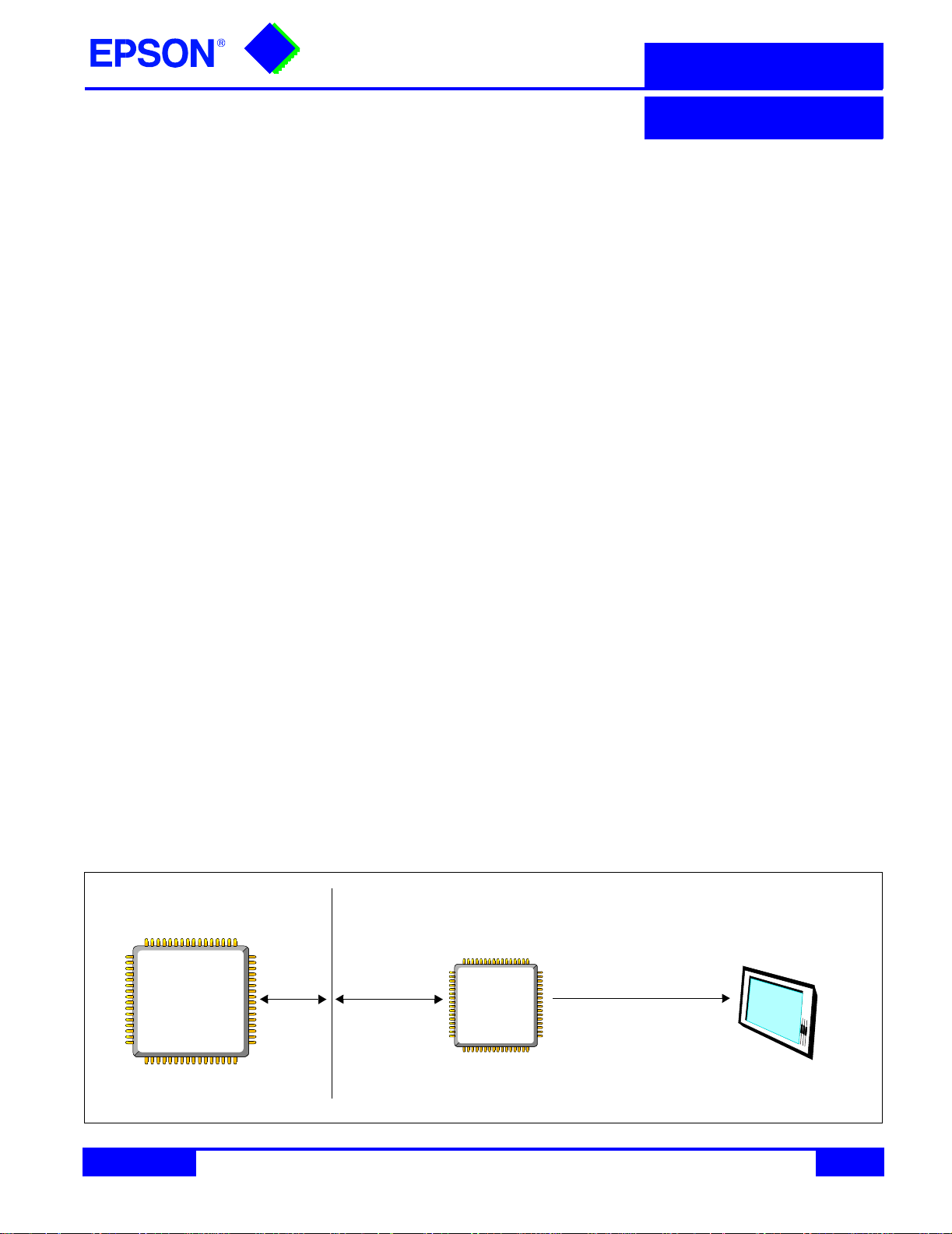
■ SYSTEM BLOCK DIAGRAM
• Up to 256 simultaneous colors from a possible
4096 colors on passive LCD panels and active
matrix TFT/D-TFD LCD panels.
• Register level support for EL panels.
• Hardware Portrait Mode
• Split Screen Display
• Virtual Display Support
• LCD power-down sequencing.
CPU
X27A-C-001-04 1
Data and
Control Signals
S1D13705
Digital Out
Flat Panel
Page 6

GRAPHICS
S1D13705
■ DESCRIPTION
Memory Interface
• Embedded 80K byte SRAM display buffer.
CPU Interface
• Direct support for:
Hitachi SH-3.
Hitachi SH-4.
Motorola M68xxx.
MPU bus interface with programmable READY.
• CPU write buffer.
Display Support
• 4/8-bit monochrome LCD interface.
• 4/8-bit color LCD interface.
• Single-panel, single-drive passive displays.
• Dual-panel, dual-drive passive displays.
• Active matrix TFT / D-TFD interface.
• Example resolutio ns:
640x480 at a color depth of 2 bpp.
640x240 at a color depth of 4 bpp.
320x240 at a color depth of 8 bpp.
Clock Source
• Single clock input for both pixel and memory clocks.
• The S1D13705 clock source can be internally divided
down for a higher frequency clock input.
• Dynamic switching of m emory clocks in portrait mode.
Display Modes
• 1/2/4/8 bit-per-pixel (bpp) support on LCD.
• Up to 16 shades of gray using FRM on
monochrome passive LCD panels.
• Up to 256 simultaneous colors from a possible 4096
colors on passive STN and active matrix TFT/D-TFD
LCD panels.
• Split Screen Display: a llows two differen t images to be
simultaneously viewed on the same display.
• Virtual Display Support: displays images larger than
the display size through the use of panning.
• Double Buffering/multi-pages: provides smooth
animation and instantaneous screen update.
• Hardware Portrait Mode: direct hardware 90°
rotation of display image for portrait mode dis play.
Power Down Modes
• Software Suspend mode.
• LCD power-down sequencing.
Operating Voltage
• CORE
2.7 to 3.6 volts; IO
VDD
2.7 to 5.5 volts.
VDD
Package
• 80-pin QFP 14.
CONTACT YOUR SALES REPRESENTATIVE FOR THESE
COMPREHENSIVE DESIGN TOOLS:
• S1D13705 Technical Manual
• S5U13705 Evaluation Boards
• Windows
CE Display Driver
• CPU Independent Software Utilities
Japan
Seiko Epson Corporation
Electronic Devices Marketing Division
421-8, Hino, Hino-shi
Tokyo 191-8501, Japan
Tel: 042-587-5812
Fax: 042-587-5564
http://www.epson.co.jp
Hong Kong
Epson Hong Kong Ltd.
20/F., Harbour Centre
25 Harbour Road
Wanchai, Hong Kong
Tel: 2585-4600
Fax: 2827-4346
Copyright © 2001 Epson Research and Development, Inc. All rights reserved. VDC
Information in this document is subject to chang e w ithout no tice. Y ou may do wnl oad an d use this docu ment, but only for your ow n use in evaluating Seiko Epson/
EPSON products. You may not modify the document. Epson Research and Development, Inc. disclaims any re presentati on that the contents of this document are
accurate or current. The Programs/Technologies described in this document may contain material protected under U.S. and/or International Patent laws.
EPSON is a registered trademark of Seiko Epson Corporation. Microsoft, Windows, and the Windows CE Logo are registere d trademarks of Microsoft Corporation.
North America
Epson Electronics America, Inc.
150 River Oaks Parkway
San Jose, CA 95134, USA
Tel: (408) 922-0200
Fax: (408) 922-0238
http://www.eea.epson.com
Europe
Epson Europe Electronics GmbH
Riesstrasse 15
80992 Munich, Germany
Tel: 089-14005-0
Fax: 089-14005-110
FOR SYSTEM INTEGRATION SERVICES
FOR WINDOWS® CE CONTACT:
Epson Research & Development, Inc.
Suite #320 - 11120 Horseshoe Way
Richmond, B.C., Canada V7A 5H7
Tel: (604) 275-5151
Fax: (604) 275-2167
Email: wince@erd.epson.com
http://www.erd.epson.com
Taiwan
Epson Taiwan Technology
& Trading Ltd.
10F, No. 287
Nanking East Road
Sec. 3, Taipei, Taiwan
Tel: 02-2717-7360
Fax: 02-2712-9164
Singapore
Epson Singapore Pte., Ltd.
No. 1
Temasek Avenue #36-00
Millenia Tower
Singapore, 039192
Tel: 337-7911
Fax: 334-2716
X27A-C-001-04 2
Page 7

S1D13705 Embedded Memory LCD Controller
Hardware Functional Specification
Document Number: X27A-A-001-10
Copyright © 1999, 2002 Epson Research and Development, Inc. All Rights Reser ved.
Information in this document is subject to change without notice. You may download and use this document, but only for your own use in
evaluating Seiko Epson/EPSON products. You may not modify the document. Epson Research and Development, Inc. disclaims any
representation that the contents of this document are accurate or current. The Programs/Technologies described in this document may contain
material protected under U.S. and/or International Patent laws.
EPSON is a registered trademark of Seiko Epson Corporation. All other Trademarks are the property of their respective owners
Page 8

Page 2 Epson Research and Development
Vancouver Design Center
THIS PA GE LEFT BLANK
S1D13705 Hardware Functional Specification
X27A-A-001-10 Issue Date: 02/02/01
Page 9

Epson Research and Development Page 3
Vancouver Design Center
Table of Contents
1 Introduction . . . . . . . . . . . . . . . . . . . . . . . . . . . . . . . . . . . . . . . . 9
1.1 Scope . . . . . . . . . . . . . . . . . . . . . . . . . . . . . . . . . . .9
1.2 Overview Description . . . . . . . . . . . . . . . . . . . . . . . . . . . . 9
2 Features . . . . . . . . . . . . . . . . . . . . . . . . . . . . . . . . . . . . . . . . . 10
2.1 Integrated Frame Buffer . . . . . . . . . . . . . . . . . . . . . . . . . . 10
2.2 CPU Interface . . . . . . . . . . . . . . . . . . . . . . . . . . . . . . 10
2.3 Display Support . . . . . . . . . . . . . . . . . . . . . . . . . . . . . . 10
2.4 Display Modes . . . . . . . . . . . . . . . . . . . . . . . . . . . . . . 11
2.5 Clock Source . . . . . . . . . . . . . . . . . . . . . . . . . . . . . . . 11
2.6 Miscellaneous . . . . . . . . . . . . . . . . . . . . . . . . . . . . . . 11
2.7 Package . . . . . . . . . . . . . . . . . . . . . . . . . . . . . . . . . 11
3 Typical System Implementation Diagrams . . . . . . . . . . . . . . . . . . . . . . 12
4 Functional Block Diagram . . . . . . . . . . . . . . . . . . . . . . . . . . . . . . . 15
4.1 Functional Block Descriptions . . . . . . . . . . . . . . . . . . . . . . . . 15
4.1.1 Host Interface . . . . . . . . . . . . . . . . . . . . . . . . . . . . . . . . . . . . . 15
4.1.2 Memory Controller . . . . . . . . . . . . . . . . . . . . . . . . . . . . . . . . . . 15
4.1.3 Sequence Controller . . . . . . . . . . . . . . . . . . . . . . . . . . . . . . . . . . 15
4.1.4 Look-Up Table . . . . . . . . . . . . . . . . . . . . . . . . . . . . . . . . . . . . 16
4.1.5 LCD Interface . . . . . . . . . . . . . . . . . . . . . . . . . . . . . . . . . . . . . 16
4.1.6 Power Save . . . . . . . . . . . . . . . . . . . . . . . . . . . . . . . . . . . . . . 16
5 Pins . . . . . . . . . . . . . . . . . . . . . . . . . . . . . . . . . . . . . . . . . . . 17
5.1 Pinout Diagram . . . . . . . . . . . . . . . . . . . . . . . . . . . . . . 17
5.2 Pin Description . . . . . . . . . . . . . . . . . . . . . . . . . . . . . . 18
5.2.1 Host Interface . . . . . . . . . . . . . . . . . . . . . . . . . . . . . . . . . . . . . 18
5.2.2 LCD Interface . . . . . . . . . . . . . . . . . . . . . . . . . . . . . . . . . . . . . 20
5.2.3 Clock Input . . . . . . . . . . . . . . . . . . . . . . . . . . . . . . . . . . . . . . 21
5.2.4 Miscellaneous . . . . . . . . . . . . . . . . . . . . . . . . . . . . . . . . . . . . . 21
5.2.5 Power Supply . . . . . . . . . . . . . . . . . . . . . . . . . . . . . . . . . . . . . 21
5.3 Summary of Configuration Options . . . . . . . . . . . . . . . . . . . . . . 22
5.4 Host Bus Interface Pin Mapping . . . . . . . . . . . . . . . . . . . . . . . 22
5.5 LCD Interface Pin Mapping . . . . . . . . . . . . . . . . . . . . . . . . . 23
6 D.C. Characteristics . . . . . . . . . . . . . . . . . . . . . . . . . . . . . . . . . . 24
7 A.C. Characteristics . . . . . . . . . . . . . . . . . . . . . . . . . . . . . . . . . . 26
7.1 Bus Interface Timing . . . . . . . . . . . . . . . . . . . . . . . . . . . 26
7.1.1 SH-4 Interface Timing . . . . . . . . . . . . . . . . . . . . . . . . . . . . . . . . 26
7.1.2 SH-3 Interface Timing . . . . . . . . . . . . . . . . . . . . . . . . . . . . . . . . 28
7.1.3 Motorola MC68K #1 Interface Timing . . . . . . . . . . . . . . . . . . . . . . . . 30
7.1.4 Motorola MC68K #2 Interface Timing . . . . . . . . . . . . . . . . . . . . . . . . 31
Hardware Functional Specification S1D13705
Issue Date: 02/02/01 X27A-A-001-10
Page 10

Page 4 Epson Research and Development
Vancouver Design Center
7.1.5 Generic #1 Interface Timing . . . . . . . . . . . . . . . . . . . . . . . . . . . . . . 32
7.1.6 Generic #2 Interface Timing . . . . . . . . . . . . . . . . . . . . . . . . . . . . . . 33
7.2 Clock Input Requirements . . . . . . . . . . . . . . . . . . . . . . . . . .34
7.3 Display Interface . . . . . . . . . . . . . . . . . . . . . . . . . . . . . .36
7.3.1 Power On/Reset Timing . . . . . . . . . . . . . . . . . . . . . . . . . . . . . . . . 36
7.3.2 Power Down/Up Timing . . . . . . . . . . . . . . . . . . . . . . . . . . . . . . . 37
7.3.3 Single Monochrome 4-Bit Panel Timing . . . . . . . . . . . . . . . . . . . . . . . 38
7.3.4 Single Monochrome 8-Bit Panel Timing . . . . . . . . . . . . . . . . . . . . . . . 40
7.3.5 Single Color 4-Bit Panel Timing . . . . . . . . . . . . . . . . . . . . . . . . . . . 42
7.3.6 Single Color 8-Bit Panel Timing (Format 1) . . . . . . . . . . . . . . . . . . . . . 44
7.3.7 Single Color 8-Bit Panel Timing (Format 2) . . . . . . . . . . . . . . . . . . . . . 46
7.3.8 Dual Monochrome 8-Bit Panel Timing . . . . . . . . . . . . . . . . . . . . . . . . 48
7.3.9 Dual Color 8-Bit Panel Timing . . . . . . . . . . . . . . . . . . . . . . . . . . . . 50
7.3.10 9/12-Bit TFT/D-TFD Panel Timing . . . . . . . . . . . . . . . . . . . . . . . . . . 52
8 Registers . . . . . . . . . . . . . . . . . . . . . . . . . . . . . . . . . . . . . . . . .55
8.1 Register Mapping . . . . . . . . . . . . . . . . . . . . . . . . . . . . .55
8.2 Register Descriptions . . . . . . . . . . . . . . . . . . . . . . . . . . . .55
9 Frame Rate Calculation . . . . . . . . . . . . . . . . . . . . . . . . . . . . . . . . .69
10 Display Data Formats . . . . . . . . . . . . . . . . . . . . . . . . . . . . . . . . . .70
11 Look-Up Table Architectur e . . . . . . . . . . . . . . . . . . . . . . . . . . . . . . .71
11.1 Monochrome Modes . . . . . . . . . . . . . . . . . . . . . . . . . . . .71
11.2 Color Modes . . . . . . . . . . . . . . . . . . . . . . . . . . . . . . .73
12 SwivelView™ . . . . . . . . . . . . . . . . . . . . . . . . . . . . . . . . . . . . . . .77
12.1 Default SwivelView Mode . . . . . . . . . . . . . . . . . . . . . . . . . .77
12.1.1 How to Set Up Default SwivelView Mode . . . . . . . . . . . . . . . . . . . . . . 78
12.2 Alternate SwivelView Mode . . . . . . . . . . . . . . . . . . . . . . . . .79
12.2.1 How to Set Up Alternate SwivelView Mode . . . . . . . . . . . . . . . . . . . . . 80
12.3 Comparison Between Default and Alternate SwivelView Modes . . . . . . . . . . .81
12.4 SwivelView Mode Limitations . . . . . . . . . . . . . . . . . . . . . . . .81
13 Power Save Modes . . . . . . . . . . . . . . . . . . . . . . . . . . . . . . . . . . . .82
13.1 Software Power Save Mode . . . . . . . . . . . . . . . . . . . . . . . . .82
13.2 Hardware Power Save Mode . . . . . . . . . . . . . . . . . . . . . . . . .82
13.3 Power Save Mode Function Summary . . . . . . . . . . . . . . . . . . . . .83
13.4 Panel Power Up/Down Sequence . . . . . . . . . . . . . . . . . . . . . . .83
13.5 Turning Off BCLK Between Accesses . . . . . . . . . . . . . . . . . . . . .84
13.6 Clock Requirements . . . . . . . . . . . . . . . . . . . . . . . . . . . .85
14 Mechanical Data . . . . . . . . . . . . . . . . . . . . . . . . . . . . . . . . . . . . .86
15 Sales and Technical Support . . . . . . . . . . . . . . . . . . . . . . . . . . . . . .87
S1D13705 Hardware Functional Specification
X27A-A-001-10 Issue Date: 02/02/01
Page 11

Epson Research and Development Page 5
Vancouver Design Center
List of Tables
Table 5-1: Summary of Power On/Reset Options . . . . . . . . . . . . . . . . . . . . . . . . . . . 22
Table 5-2: Host Bus Interface Pin Mapping . . . . . . . . . . . . . . . . . . . . . . . . . . . . . . 22
Table 5-3: LCD Interface Pin Mapping . . . . . . . . . . . . . . . . . . . . . . . . . . . . . . . . 23
Table 6-1: Absolute Maximum Ratings . . . . . . . . . . . . . . . . . . . . . . . . . . . . . . . . 24
Table 6-2: Recommended Operating Conditions for Core VDD = 3.3V ± 10% . . . . . . . . . . . 24
Table 6-3: Input Specifications . . . . . . . . . . . . . . . . . . . . . . . . . . . . . . . . . . . . 24
Table 6-4: Output Specifications. . . . . . . . . . . . . . . . . . . . . . . . . . . . . . . . . . . . 25
Table 7-1: SH-4 Timing . . . . . . . . . . . . . . . . . . . . . . . . . . . . . . . . . . . . . . . . 27
Table 7-2: SH-3 Bus Timing. . . . . . . . . . . . . . . . . . . . . . . . . . . . . . . . . . . . . . 29
Table 7-3: MC68K #1 Bus Timing (MC68000) . . . . . . . . . . . . . . . . . . . . . . . . . . . 30
Table 7-4: MC68K #2 Timing (MC68030) . . . . . . . . . . . . . . . . . . . . . . . . . . . . . . 31
Table 7-5: Generic #1 Timing . . . . . . . . . . . . . . . . . . . . . . . . . . . . . . . . . . . . . 32
Table 7-6: Generic #2 Timing . . . . . . . . . . . . . . . . . . . . . . . . . . . . . . . . . . . . . 33
Table 7-7: Clock Input Requirements for CLKI. . . . . . . . . . . . . . . . . . . . . . . . . . . . 34
Table 7-8: Clock Input Requirements for BCLK . . . . . . . . . . . . . . . . . . . . . . . . . . . 35
Table 7-9: LCD Panel Power On/Reset Timing . . . . . . . . . . . . . . . . . . . . . . . . . . . . 36
Table 7-10: Power Down/Up Timing . . . . . . . . . . . . . . . . . . . . . . . . . . . . . . . . . . 37
Table 7-11: Single Monochrome 4-Bit Panel A.C. Timing. . . . . . . . . . . . . . . . . . . . . . . 39
Table 7-12: Single Monochrome 8-Bit Panel A.C. Timing. . . . . . . . . . . . . . . . . . . . . . . 41
Table 7-13: Single Color 4-Bit Panel A.C. Timing . . . . . . . . . . . . . . . . . . . . . . . . . . . 43
Table 7-14: Single Color 8-Bit Panel A.C. Timing (Format 1) . . . . . . . . . . . . . . . . . . . . . 45
Table 7-15: Single Color 8-Bit Panel A.C. Timing (Format 2) . . . . . . . . . . . . . . . . . . . . . 47
Table 7-16: Dual Monochrome 8-Bit Panel A.C. Timing. . . . . . . . . . . . . . . . . . . . . . . . 49
Table 7-17: Dual Color 8-Bit Panel A.C. Timing. . . . . . . . . . . . . . . . . . . . . . . . . . . . 51
Table 7-18: TFT/D-TFD A.C. Timing . . . . . . . . . . . . . . . . . . . . . . . . . . . . . . . . . 54
Table 8-1: Panel Data Format . . . . . . . . . . . . . . . . . . . . . . . . . . . . . . . . . . . . . 56
Table 8-2: Gray Scale/Color Mode Selection . . . . . . . . . . . . . . . . . . . . . . . . . . . . . 57
Table 8-3: High Performance Selection . . . . . . . . . . . . . . . . . . . . . . . . . . . . . . . . 57
Table 8-4: Inverse Video Mode Select Options . . . . . . . . . . . . . . . . . . . . . . . . . . . . 58
Table 8-5: Hardware Power Save/GPIO0 Operation . . . . . . . . . . . . . . . . . . . . . . . . . 59
Table 8-6: Software Power Save Mode Selection . . . . . . . . . . . . . . . . . . . . . . . . . . . 59
Table 8-7: Selection of SwivelView Mode . . . . . . . . . . . . . . . . . . . . . . . . . . . . . . 67
Table 8-8: Selection of PCLK and MCLK in SwivelView Mode. . . . . . . . . . . . . . . . . . . 68
Table 12-1: Default and Alternate SwivelView Mode Comparison . . . . . . . . . . . . . . . . . . 81
Table 13-1: Power Save Mode Selection . . . . . . . . . . . . . . . . . . . . . . . . . . . . . . . . 82
Table 13-2: Software Power Save Mode Summary. . . . . . . . . . . . . . . . . . . . . . . . . . . 82
Table 13-3: Hardware Power Save Mode Summary . . . . . . . . . . . . . . . . . . . . . . . . . . 82
Table 13-4: Power Save Mode Function Summary . . . . . . . . . . . . . . . . . . . . . . . . . . . 83
Table 13-5: S1D13705 Internal Clock Requirements. . . . . . . . . . . . . . . . . . . . . . . . . . 85
Hardware Functional Specification S1D13705
Issue Date: 02/02/01 X27A-A-001-10
Page 12

Page 6 Epson Research and Development
Vancouver Design Center
THIS PA GE LEFT BLANK
S1D13705 Hardware Functional Specification
X27A-A-001-10 Issue Date: 02/02/01
Page 13

Epson Research and Development Page 7
Vancouver Design Center
List of Figures
Figure 3-1: Typical System Diagram (SH-4 Bus). . . . . . . . . . . . . . . . . . . . . . . . . . . .12
Figure 3-2: Typical System Diagram (SH-3 Bus). . . . . . . . . . . . . . . . . . . . . . . . . . . .12
Figure 3-3: Typical System Diagram (M68K #1 Bus) . . . . . . . . . . . . . . . . . . . . . . . . .13
Figure 3-4: Typical System Diagram (M68K #2 Bus) . . . . . . . . . . . . . . . . . . . . . . . . .13
Figure 3-5: Typical System Diagram (Generic #1 Bus) . . . . . . . . . . . . . . . . . . . . . . . .14
Figure 3-6: Typical System Diagram (Generic #2 Bus - e.g. ISA Bus). . . . . . . . . . . . . . . . .14
Figure 4-1: System Block Diagram Showing Data Paths. . . . . . . . . . . . . . . . . . . . . . . .15
Figure 5-1: Pinout Diagram . . . . . . . . . . . . . . . . . . . . . . . . . . . . . . . . . . . . . . .17
Figure 7-1: SH-4 Timing . . . . . . . . . . . . . . . . . . . . . . . . . . . . . . . . . . . . . . . .26
Figure 7-2: SH-3 Bus Timing . . . . . . . . . . . . . . . . . . . . . . . . . . . . . . . . . . . . . .28
Figure 7-3: MC68K #1 Bus Timing (MC68000) . . . . . . . . . . . . . . . . . . . . . . . . . . . .30
Figure 7-4: MC68K #2 Timing (MC68030) . . . . . . . . . . . . . . . . . . . . . . . . . . . . . .31
Figure 7-5: Generic #1 Timing . . . . . . . . . . . . . . . . . . . . . . . . . . . . . . . . . . . . .32
Figure 7-6: Generic #2 Timing . . . . . . . . . . . . . . . . . . . . . . . . . . . . . . . . . . . . .33
Figure 7-7: Clock Input Requirements for CLKI . . . . . . . . . . . . . . . . . . . . . . . . . . . .34
Figure 7-8: Clock Input Requirements for BCLK . . . . . . . . . . . . . . . . . . . . . . . . . . .35
Figure 7-9: LCD Panel Power On/Reset Timing . . . . . . . . . . . . . . . . . . . . . . . . . . . .36
Figure 7-10: Power Down/Up Timing . . . . . . . . . . . . . . . . . . . . . . . . . . . . . . . . . .37
Figure 7-11: Single Monochrome 4-Bit Panel Timing. . . . . . . . . . . . . . . . . . . . . . . . . .38
Figure 7-12: Single Monochrome 4-Bit Panel A.C. Timing . . . . . . . . . . . . . . . . . . . . . . .39
Figure 7-13: Single Monochrome 8-Bit Panel Timing. . . . . . . . . . . . . . . . . . . . . . . . . .40
Figure 7-14: Single Monochrome 8-Bit Panel A.C. Timing . . . . . . . . . . . . . . . . . . . . . . .41
Figure 7-15: Single Color 4-Bit Panel Timing . . . . . . . . . . . . . . . . . . . . . . . . . . . . . .42
Figure 7-16: Single Color 4-Bit Panel A.C. Timing . . . . . . . . . . . . . . . . . . . . . . . . . . .43
Figure 7-17: Single Color 8-Bit Panel Timing (Format 1). . . . . . . . . . . . . . . . . . . . . . . .44
Figure 7-18: Single Color 8-Bit Panel A.C. Timing (Format 1) . . . . . . . . . . . . . . . . . . . . .45
Figure 7-19: Single Color 8-Bit Panel Timing (Format 2). . . . . . . . . . . . . . . . . . . . . . . .46
Figure 7-20: Single Color 8-Bit Panel A.C. Timing (Format 2) . . . . . . . . . . . . . . . . . . . . .47
Figure 7-21: Dual Monochrome 8-Bit Panel Timing. . . . . . . . . . . . . . . . . . . . . . . . . . .48
Figure 7-22: Dual Monochrome 8-Bit Panel A.C. Timing. . . . . . . . . . . . . . . . . . . . . . . .49
Figure 7-23: Dual Color 8-Bit Panel Timing. . . . . . . . . . . . . . . . . . . . . . . . . . . . . . .50
Figure 7-24: Dual Color 8-Bit Panel A.C. Timing . . . . . . . . . . . . . . . . . . . . . . . . . . . .51
Figure 7-25: 12-Bit TFT/D-TFD Panel Timing . . . . . . . . . . . . . . . . . . . . . . . . . . . . .52
Figure 7-26: TFT/D-TFD A.C. Timing. . . . . . . . . . . . . . . . . . . . . . . . . . . . . . . . . .53
Figure 8-1: Screen-Register Relationship, Split Screen . . . . . . . . . . . . . . . . . . . . . . . . .65
Figure 10-1: 1/2/4/8 Bit-Per-Pixel Display Data Memory Organization. . . . . . . . . . . . . . . . .70
Figure 11-1: 1 Bit-per-pixel Monochrome Mode Data Output Path . . . . . . . . . . . . . . . . . . .71
Hardware Functional Specification S1D13705
Issue Date: 02/02/01 X27A-A-001-10
Page 14

Page 8 Epson Research and Development
Vancouver Design Center
Figure 11-2: 2 Bit-per-pixel Monochrome Mode Data Output Path . . . . . . . . . . . . . . . . . . .71
Figure 11-3: 4 Bit-per-pixel Monochrome Mode Data Output Path . . . . . . . . . . . . . . . . . . .72
Figure 11-4: 1 Bit-per-pixel Color Mode Data Output Path . . . . . . . . . . . . . . . . . . . . . . .73
Figure 11-5: 2 Bit-per-pixel Color Mode Data Output Path . . . . . . . . . . . . . . . . . . . . . . .74
Figure 11-6: 4 Bit-per-pixel Color Mode Data Output Path . . . . . . . . . . . . . . . . . . . . . . .75
Figure 11-7: 8 Bit-per-pixel Color Mode Data Output Path . . . . . . . . . . . . . . . . . . . . . . .76
Figure 12-1: Relationship Between The Screen Image and the Image Refreshed by
S1D13705 in Default Mode. . . . . . . . . . . . . . . . . . . . . . . . . . . . . . . . .77
Figure 12-2: Relationship Between The Screen Image and the Image Refreshed by
S1D13705 in Alternate Mode. . . . . . . . . . . . . . . . . . . . . . . . . . . . . . . .79
Figure 13-1: Panel On/Off Sequence . . . . . . . . . . . . . . . . . . . . . . . . . . . . . . . . . . .84
Figure 14-1: Mechanical Drawing QFP14 . . . . . . . . . . . . . . . . . . . . . . . . . . . . . . . .86
S1D13705 Hardware Functional Specification
X27A-A-001-10 Issue Date: 02/02/01
Page 15

Epson Research and Development Page 9
Vancouver Design Center
1 Introduction
1.1 Scope
This is the Hardware Functi onal Specifi cation for the S1 D13705 Embedded Memor y LCD
Controller Chip. Included in this document are timing diagrams, AC and DC characteristics, register descriptions, and power management descriptions. This document is
intended for two audiences: Video Subsystem Designers and Software Developers.
This document is updated as appropriate. Please check for the latest revision of this
document before beginning any development. The latest revision can be downloaded at
www.erd.epson.com.
We appreciate your comments on our documentation. Please contact us via email at
documentation@erd.epson.com.
1.2 Overview Description
The S1D13705 is a color / monochrome LCD graphics controller with an embedded 80K
byte SRAM display buffer. The high int egration of the S1D13 705 provides a low cos t, low
power, single chip solution to meet the requirements of embedded markets such as Office
Automation equipment, Mobile Communications devices, and Hand-Held PCs where
board size and battery life are major concerns.
Products requiring a “Portrait” display can take advantage of the SwivelView™ Mode
feature of the S1D13705. Virtual and Split Screen are just some of the display modes
supported. The above features, combined with the Operating System independence of the
S1D13705, make it the ideal solution for a wide variety of applications.
Hardware Functional Specification S1D13705
Issue Date: 02/02/01 X27A-A-001-10
Page 16

Page 10 Epson Research and Development
Vancouver Design Center
2 Features
2.1 Integrated Frame Buffer
• Embedded 80K byte SRAM display buffer.
2.2 CPU Interface
• Direct support of the following interfaces:
Hitachi SH-3.
Hitachi SH-4.
Motorola M68 K.
MPU bus interface using WAIT# signal.
• Direct mem ory mapping of internal r egisters.
• Single level CPU write buffer.
• Registers are mapped into upper 32 bytes of 128K byte address space.
• The complete 80K byte display buffe r is directl y and contiguou sly avai lable throu gh the
17-bit address bus.
2.3 Display Support
• 4/8-bit monochrome LCD interface.
• 4/8-bit color LCD interface.
• Single-panel, single-drive passive displays.
• Dual-panel, dual-drive passive displays.
• Active Matrix TFT / D-TFD interface
• Register level support for EL panels.
• Example resolutions:
640x480 at a color depth of 2 bpp
640x240 at a color depth of 4 bpp
320x240 at a color depth of 8 bpp
S1D13705 Hardware Functional Specification
X27A-A-001-10 Issue Date: 02/02/01
Page 17

Epson Research and Development Page 11
Vancouver Design Center
2.4 Display Modes
• SwivelView™: direct 90° hardware rotation of display image for portrait mode display
• 1/2/4 bit-per-pixel (bpp), 2/4/16-level grayscale display.
• 1/2/4/8 bit-per-pixel, 2/4/16/256-level color display.
• Up to 16 shades of gray by FRM on monochrome passive LCD panels; a 256x4 LookUp Table is used to map 1/2/4 bpp modes into these shades.
• 256 simultaneous of 4096 colors on color passive and active matrix LCD panels; three
256x4 Look-Up Tables are used to map 1/2/4/8 bpp modes into these colors.
• Split screen display for all landscape panel modes allows two different images to be
simultaneously displa yed.
• Virtual display support (displays images larger than the panel size through the use of
panning).
2.5 Clock Source
• Maximum operating clock (CLK) frequency of 25MHz.
• Operating clock (CLK) is derived from CLKI input.
• Pixel Clock (PCLK) and Memory Clock (MCLK) are derived from CLK.
2.6 Miscellaneous
• Hardware/Software Video Invert.
• Softwar e Power Save mode.
• Hardware Power Save mode.
• LCD power-down sequencing.
• 5 General Purpose Input/Output pins are available.
• Core operates from 2.7 volts to 3.6 volts.
CLK = CLKI
or
CLK = CLKI/2
• GPIO0 is available if Hardware Power Save is not required.
• GPIO[4:1] are available if upper LCD data pins (FPDAT[11:8]) are not required for
TFT/D-TFD support or hardware inverse video.
• IO Operates from the core voltag e up to 5.5 volts.
2.7 Package
• 80 pin QFP14 package.
Hardware Functional Specification S1D13705
Issue Date: 02/02/01 X27A-A-001-10
Page 18
Page 12 Epson Research and Development
Vancouver Design Center
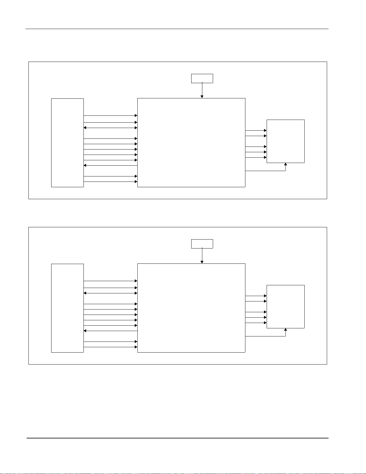
3 Typical System Implementation Diagrams
.
Oscillator
SH-4
BUS
SH-3
BUS
CSn#
A[16:0]
D[15:0]
WE1#
BS#
RD/WR#
RD#
WE0#
RDY#
CKIO
RESET#
CSn#
A[16:0]
D[15:0]
WE1#
BS#
RD/WR#
RD#
WE0#
WAIT#
CKIO
RESET#
CLKI
CS#
AB[16:0]
DB[15:0]
WE1#
BS#
RD/WR#
RD#
WE0#
WAIT#
BCLK
RESET#
S1D13705
FPDAT[7:0]
FPSHIFT
FPFRAME
FPLINE
DRDY
LCDPWR
Figure 3-1: Typical System Diagram (SH-4 Bus)
.
Oscillator
CLKI
CS#
AB[16:0]
DB[15:0]
WE1#
BS#
RD/WR#
RD#
WE0#
WAIT#
BCLK
RESET#
S1D13705
FPDAT[7:4]
FPSHIFT
FPFRAME
FPLINE
DRDY
LCDPWR
D[7:0]
FPSHIFT
FPFRAME
FPLINE
MOD
D[3:0]
FPSHIFT
FPFRAME
FPLINE
MOD
8-bit
LCD
Display
4-bit
LCD
Display
Figure 3-2: Typical System Diagram (SH-3 Bus)
S1D13705 Hardware Functional Specification
X27A-A-001-10 Issue Date: 02/02/01
Page 19
Epson Research and Development Page 13
Vancouver Design Center
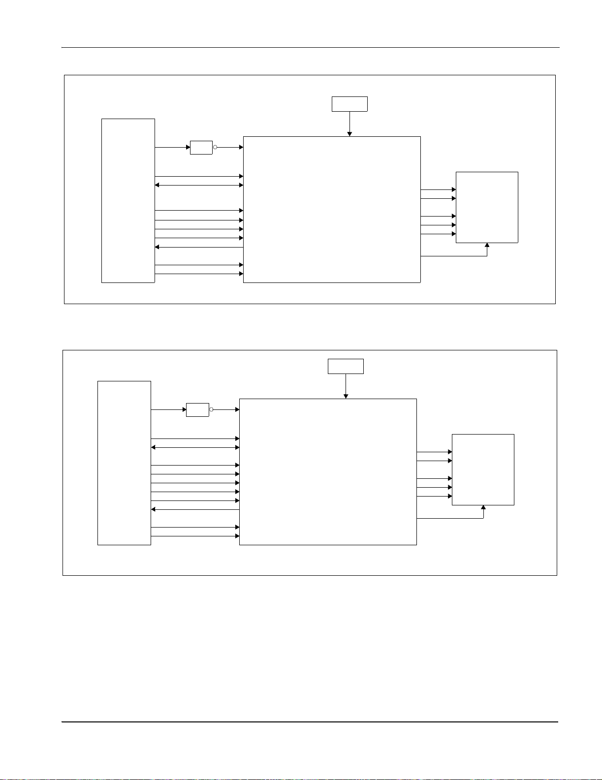
.
Oscillator
MC68000
BUS
A[23:17]
FC0, FC1, FC2
Decoder
CS#
CLKI
MC68030
BUS
A[31:17]
FC0, FC1, FC2
D[31:16]
DSACK1#
RESET#
A[16:1]
D[15:0]
LDS#
UDS#
AS#
R/W#
DTACK#
CLK
RESET#
A[16:0]
DS#
AS#
R/W#
SIZ1
SIZ0
CLK
AB[16:1]
DB[15:0]
AB0
WE1#
BS#
RD/WR#
WAIT#
BCLK
RESET#
S1D13705
FPDAT[7:4]
FPSHIFT
FPFRAME
FPLINE
LCDPWR
Figure 3-3: Typical System Diagram (M68K #1 Bus)
.
Oscillator
Decoder
CS#
AB[16:0]
DB[15:0]
WE1#
BS#
RD/WR#
RD#
WE0#
WAIT#
BCLK
RESET#
S1D13705
CLKI
FPDAT[7:0]
FPSHIFT
FPFRAME
FPLINE
DRDY
LCDPWR
DRDY
D[3:0]
FPSHIFT
FPFRAME
FPLINE
MOD
D[7:0]
FPSHIFT
FPFRAME
FPLINE
MOD
4-bit
LCD
Display
8-bit
LCD
Display
Figure 3-4: Typical System Diagram (M68K #2 Bus)
Hardware Functional Specification S1D13705
Issue Date: 02/02/01 X27A-A-001-10
Page 20
Page 14 Epson Research and Development
Vancouver Design Center
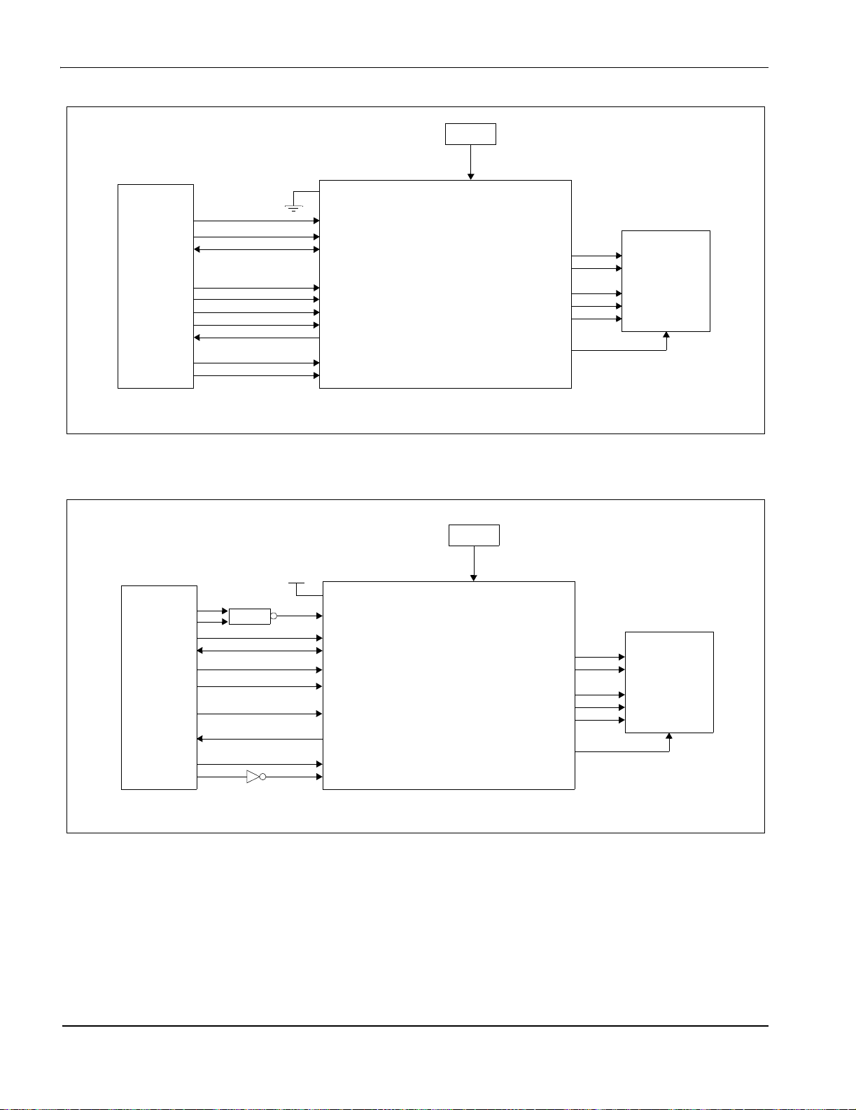
.
Oscillator
GENERIC #1
BUS
ISA
BUS
CSn#
A[16:0]
D[15:0]
WE0#
WE1#
RD0#
RD1#
WAIT#
BCLK
RESET#
REFRESH
SA[19:17]
SA[16:0]
SD[15:0]
SMEMW#
SMEMR#
SBHE#
IOCHRDY
BCLK
RESET
BS#
CS#
AB[16:0]
DB[15:0]
WE0#
WE1#
RD
RD/WR#
WAIT#
BCLK
RESET#
S1D13705
CLKI
FPDAT[11:0]
FPSHIFT
FPFRAME
FPLINE
LCDPWR
Figure 3-5: Typical System Diagram (Generic #1 Bus)
.
Oscillator
Decoder
BS#
CS#
AB[16:0]
DB[15:0]
WE0#
RD#
WE1#
WAIT#
BCLK
RESET#
S1D13705
CLKI
FPDAT[8:0]
FPSHIFT
FPFRAME
FPLINE
LCDPWR
DRDY
DRDY
D[11:0]
FPSHIFT
FPFRAME
FPLINE
DRDY
D[8:0]
FPSHIFT
FPFRAME
FPLINE
DRDY
12-bit
TFT
Display
9-bit
TFT
Display
Figure 3-6: Typical System Diagram (Generic #2 Bus - e.g. ISA Bus)
S1D13705 Hardware Functional Specification
X27A-A-001-10 Issue Date: 02/02/01
Page 21
Epson Research and Development Page 15
Vancouver Design Center
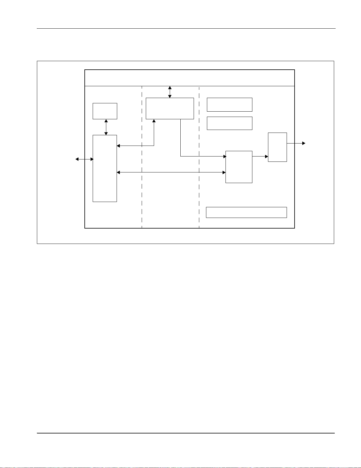
4 Functional Block Diagram
40k x 16-bit SRAM
Memory
Controller
Generic MPU
MC68K
SH-3
SH-4
Register
Host
I/F
Bus Clock Memory Clock Pixel Clock
Figure 4-1: System Block Diagram Showing Data Paths
4.1 Functional Block Descriptions
Power Save
Clocks
Look-Up
Table
Sequence Controller
LCD
I/F
LCD
4.1.1 Host Interface
The Host Interface p rovides t he mean s for the CPU/MPU to c ommunicate wi th the displ ay
buffer and internal registers.
4.1.2 Memory Contro ll er
The Memory Controller arbitrates between CPU accesses and display refresh accesses. It
also gene rates the necessary signa ls to control the SRAM fr ame buffer.
4.1.3 Sequence Controller
The Sequence Controller controls data flow from the Memory Controller throug h the LookUp Table and to the LCD Interf ace. It als o genera tes memory addresses for displa y refres h
accesses.
Hardware Functional Specification S1D13705
Issue Date: 02/02/01 X27A-A-001-10
Page 22

Page 16 Epson Research and Development
Vancouver Design Center
4.1.4 Look-Up Table
The Look-Up Table contains thr ee 256x4 Look-Up Tables or pal ettes, one for each primary
color. In monochrome mode only the green Look-Up Table is used.
4.1.5 LCD Interface
The LCD Interface performs frame rate modulation for passive LCD panels. It also
generates the correct data format and timing control signals for various LCD and
TFT/D-TFD panels.
4.1.6 Power Save
Power Save contains the power save mode circuitry.
S1D13705 Hardware Functional Specification
X27A-A-001-10 Issue Date: 02/02/01
Page 23
Epson Research and Development Page 17
Vancouver Design Center
5 Pins
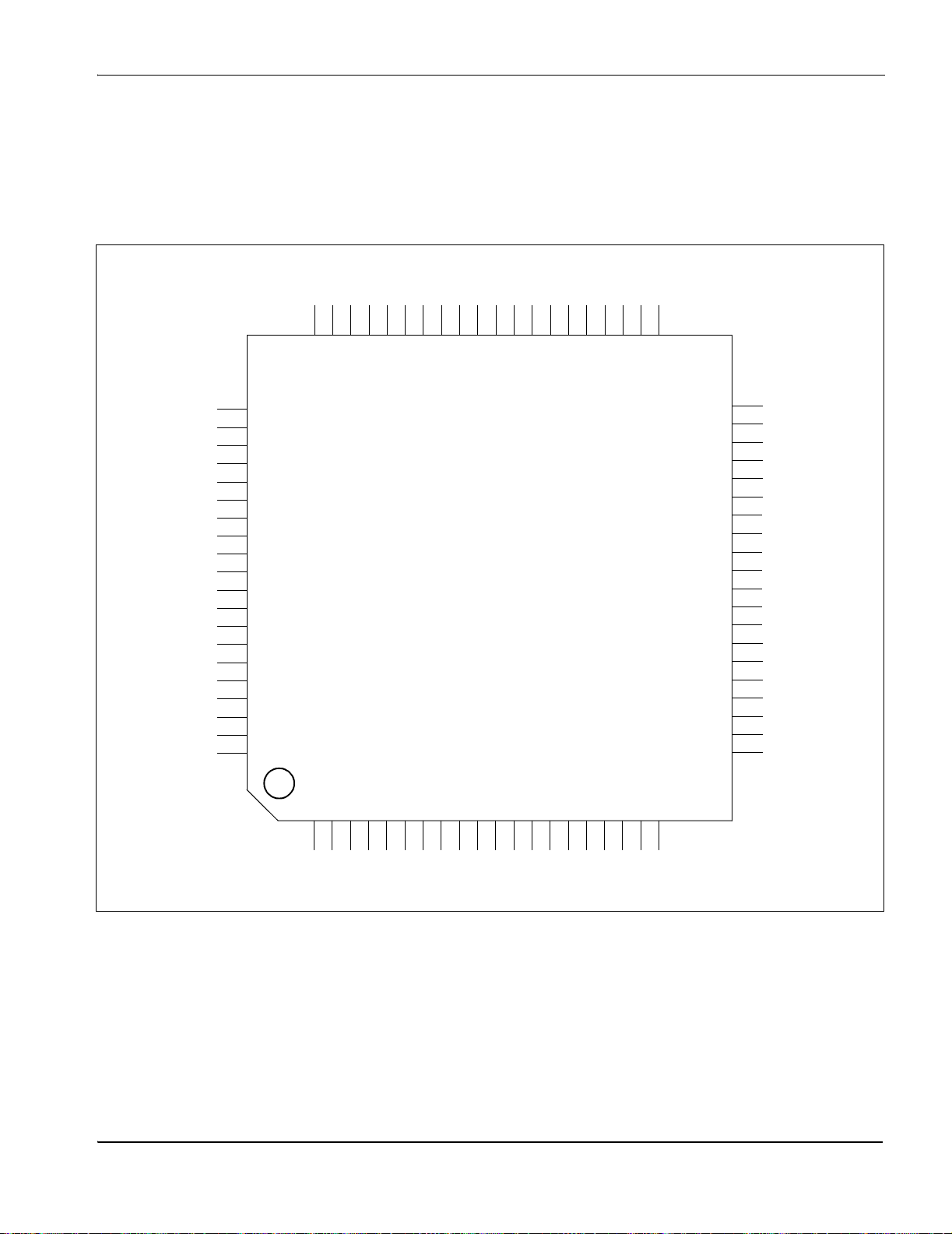
5.1 Pinout Diagram
60 59 58 57 56 55 54 53 52 51 50 49 48 47 46 45 44 43 42 41
AB11
AB9
AB10
VSS
AB12
AB13
AB14
AB15
VSS
CLKI
IOVDD
CNF1
CNF0
CNF2
CNF3
AB16
TESTEN
COREVDD
LCDPWR
DRDY
61
62
63
64
65
66
67
68
69
70
71
72
73
74
75
76
77
78
79
80
COREVDD
AB8
AB7
AB6
AB5
AB4
AB3
AB2
AB1
AB0
BCLK
VSS
RESET#
CS#
BS#
RD#
WE0#
WE1#
RD/WR#
VSS
S1D13705
COREVDD
WAIT#
DB15
1234567891011121314151617181920
DB14
DB13
DB12
DB11
DB10
IOVDD
DB9
DB7
DB6
DB5
DB4
DB3
DB8
DB2
VSS
DB0
DB1
VSS
FPFRAME
FPLINE
FPDAT0
FPDAT1
FPDAT2
FPDAT3
FPDAT4
FPDAT5
FPDAT6
FPDAT7
IOVDD
FPSHIFT
VSS
FPDAT8
FPDAT9
FPDAT10
FPDAT11
GPIO0
COREVDD
40
39
38
37
36
35
34
33
32
31
30
29
28
27
26
25
24
23
22
21
Figure 5-1: Pinout Diagram
Note
Package type: 80 pin surface mount QFP14
Hardware Functional Specification S1D13705
Issue Date: 02/02/01 X27A-A-001-10
Page 24

Page 18 Epson Research and Development
Vancouver Design Center
5.2 Pin Description
Key:
I=Input
O=Output
IO = Bi-Directional (Input/Output)
P=Power pin
C = CMOS level input
CS = CMOS level Schmitt input
COx = CMOS output driver, x denotes driver type (see I
TSx =
CNx =
TEST = CMOS level test input with pull down resistor
Tri-state CMOS output driver, x denotes driver type (see IOL/IOH in Table 6-4: “Output Specifications,” on
page 25)
CMOS low-noise outp ut dri ver, x de not es dri ve r ty pe (s ee I
page 25)
5.2.1 Host Interface
in Table 6-4: “Output Specifications,” on page 25)
OL/IOH
in Table 6-4: “Ou tpu t Sp eci fic ati on s ,” on
OL/IOH
Pin NamesTypePin #Cell
AB0 I 70 CS Input
45, 53, 54,
55, 56, 57,
AB[16:1] I
DB[15:0] IO
58, 59, 62,
63, 64, 65,
66, 67, 68,
69
3, 4, 5, 6, 7,
8, 9, 11, 12,
13, 14, 15,
16, 17, 18,
19
C/TS2 Hi-Z
RESET#
C Input These pins input the system address bits 16 through 1 (A[16:1]).
State
Description
This pin has multiple functions.
• For SH-3/SH-4 mode, this pin inputs system address bit 0
(A0).
• For MC68K #1, this pin inputs the lower data strobe (LDS#).
• For MC68K #2, this pin inputs system address bit 0 (A0).
• For Generic #1, this pin inputs system address bit 0 (A0).
• For Generic #2, this pin inputs system address bit 0 (A0).
See Table 5-2: “Host Bus Interface Pin Mapping,” on page 22
summary.
These pins have multiple functions.
• For SH-3/SH-4 mode, these pins are connected to [D15:0].
• For MC68K #1, these pins are connected to D[15:0].
• For MC68K #2, these pins are connected to D[31:16] for a
32-bit device (e.g. MC68030) or D[15:0] for a 16-bit device
(e.g. MC68340).
• For Generic #1, these pins are connected to D[15:0].
• For Generic #2, these pins are connected to D[15:0].
See Table 5-2: “Host Bus Interface Pin Mapping,” on page 22
summary.
for
for
S1D13705 Hardware Functional Specification
X27A-A-001-10 Issue Date: 02/02/01
Page 25

Epson Research and Development Page 19
Vancouver Design Center
Pin NamesTypePin #Cell
RESET#
State
Description
This pin has multiple functions.
• For SH-3/SH-4 mode, this pin inputs the write enable signal
for the lower data byte (WE0#).
• For MC68K #1, this pin must be tied to IO V
WE0# I 77 CS Input
• For MC68K #2, this pin inputs the bus size bit 0 (SIZ0).
• For Generic #1, this pin input s th e w rite enable signal for the
lower data byte (WE0#).
• For Generic #2, this pin inputs the write enable signal (WE#)
See Table 5-2: “Host Bus Interface Pin Mapping,” on page 22
summary.
This pin has multiple functions.
• For SH-3/SH-4 mode, this pin inputs the write enable signal
for the upper data byte (WE1#).
• For MC68K #1, this pin inputs the upper data strobe (UDS#).
• For MC68K #2, this pin inputs the data strobe (DS#).
WE1# I 78 CS Input
• For Generic #1, this pin input s th e w rite enable signal for the
upper data byte (WE1#).
• For Generic #2, this pin inputs the byte enable signal for the
high data byte (BHE#).
See Table 5-2: “Host Bus Interface Pin Mapping,” on page 22
summary.
CS# I 74 C Input This pin inputs the chip select signal.
BCLK I 71 C Input This pin inputs the system bus clock.
This pin has multiple functions.
• For SH-3/SH-4 mode, this pin inputs the bus start signal
(BS#).
• For MC68K #1, this pin inputs the address strobe (AS#).
BS# I 75 CS Input
• For MC68K #2, this pin inputs the address strobe (AS#).
• For Generic #1, this pin must be tied to V
• For Generic #2, this pin must be tied to IO V
See Table 5-2: “Host Bus Interface Pin Mapping,” on page 22
summary.
This pin has multiple functions.
• For SH-3/SH-4 mode, this pin inputs the RD/WR# signal.
The S1D13705 needs this signal for early decode of the bus
cycle.
• For MC68K #1, this pin inputs the R/W# signal.
RD/WR# I 79 CS Input
• For MC68K #2, this pin inputs the R/W# signal.
• For Generic #1, this pin inputs the read command for the
upper data byte (RD1#).
• For Generic #2, this pin must be tied to IO V
See Table 5-2: “Host Bus Interface Pin Mapping,” on page 22
summary.
SS
.
DD
DD
DD
for
for
.
for
.
for
Hardware Functional Specification S1D13705
Issue Date: 02/02/01 X27A-A-001-10
Page 26
Page 20 Epson Research and Development
Vancouver Design Center
Pin NamesTypePin #Cell
RESET#
RD# I 76 CS Input
WAIT# O 2 TS2 Hi-Z
RESET# I 73 CS 0
State
Description
This pin has multiple functions.
• For SH-3/SH-4 mode, this pin inputs the read signal (RD#).
• For MC68K #1, this pin must be tied to IO V
DD
.
• For MC68K #2, this pin inputs the bus size bit 1 (SIZ1).
• For Generic #1, this pin inputs the read command for the
lower data byte (RD0#).
• For Generic #2, this pin inputs the read command (RD#).
See Table 5-2: “Host Bus Interface Pin Mapping,” on page 22 for
summary.
This pin has multiple functions.
• For SH-3 mode, this pin outputs the wait request signal
(WAIT#).
• For SH-4 mode, this pin outputs the device ready signal
(RDY#).
• For MC68K #1, this pin outputs the data transfer
acknowled ge sig nal (DTACK#).
• For MC68K #2, this pin outputs the data transfer and size
acknowledge bit 1 (DSACK1#).
• For Generic #1, this pin outputs the wait signal (WAIT#).
• For Generic #2, this pin outputs the wait signal (WAIT#).
See Table 5-2: “Host Bus Interface Pin Mapping,” on page 22
for
summary.
Active low input to s et all inter nal registe rs t o the def aul t state a nd
to force all signals to their inactive states.
5.2.2 LCD Interface
Pin Name Type Pin # Cell
30, 31, 32,
FPDAT[7:0] O
33, 34, 35,
CN3 0 Panel Data
36, 37
FPDAT[10:8]
FPDAT11
O,
IO
O,
IO
24, 25, 26 CN3 Input
23 CN3 Input
FPFRAME O 39 CN3 0 Frame Pulse
RESET#
State
These pins have multiple functions.
• Panel Data bits [10:8] for TFT/D-TFD panels.
• General Purpose Input/Output pins GPIO[3:1].
These pins should be connected to IO V
See Table 5-3: “LCD Interface Pin Mapping,” on page 23
summary.
This pin has multiple functions.
• Panel Data bit 11 for TFT/D-TFD panels.
• General Purpose Input/Output pin GPIO4.
• Inverse Video select pin.
This pin should be connected to IO V
Table 5-3: “LCD Interface Pin Mapping,” on page 23
summary.
Description
when unused.
DD
when unused. See
DD
for
for
S1D13705 Hardware Functional Specification
X27A-A-001-10 Issue Date: 02/02/01
Page 27
Epson Research and Development Page 21
Vancouver Design Center
Pin Name Type Pin # Cell
RESET#
State
Description
FPLINE O 38 CN3 0 Line Pulse
FPSHIFT O 28 C N3 0 Shift Clock
LCDPWR O 43 CO1 0 Active high LCD Power Control
This pin has multiple functions.
• TFT/D-TFD Display Enable (DRDY).
DRDY O 42 CN3 0
• LCD Backplane Bias (MOD).
• Second Shift Clock (FPSHIFT2).
See Table 5-3: “LCD Interface Pin Mapping,” on page 23 for
summary.
5.2.3 Clock Input
Pin Name Type Pin # Driver Description
CLKI I 51 C Input Clock
5.2.4 Miscella neous
Pin Name Type Pin # Cell
RESET#
State
These inputs ar e used to c onfigure the S1D1 3705 - s ee Table
CNF[3:0] I
46, 47,
48, 49
C
As set by
hardware
5-1: “Summary of Power On/Reset Options,” on page 22.
Must be connected directly to IO V
This pin has multiple functions - see REG[03h] bit 2.
GPIO0
IO,
I
22
CS/
TS1
Input
• General Purpose Input/Output pin.
• Hardware Po we r Sa ve.
TESTEN I 44 TEST pulled low Test Enable input. This input must be connected to V
Description
DD
or VSS.
SS
.
5.2.5 P o w er Suppl y
Pin Name Type Pin # Driver Description
COREVDD P
IOVDD P 10, 29, 52 P IO VDD
VSS P
Hardware Functional Specification S1D13705
Issue Date: 02/02/01 X27A-A-001-10
1, 21, 41,
61
20, 27, 40,
50, 60, 72,
80
PCore V
DD
P Common VSS
Page 28
Page 22 Epson Research and Development
Vancouver Design Center
5.3 Summary of Configuration Options
Table 5-1: Summary of Power On/Reset Options
Configuration
Pin
CNF[3:0]
Select host bus interface as follows:
CNF3 CNF2 CNF1 CNF0 BS# Host Bus
1000XSH-4 interface Big Endian
0000XSH-4 interface Little Endian
1001XSH-3 interface Big Endian
0001XSH-3 interface Little Endian
X010X reserved
1011XMC68K #1, 16-bit Big Endian
0011Xreserved
X 1 0 0 X reserved
1101XMC68K #2, 16-bit Big Endian
0101Xreserved
X1100 reserved
X1101 reserved
11110 Generic #1, 16-bit Big Endian
01110 Generic #1, 16-bit Little Endian
11111 reserved
01111 Generic #2, 16-bit Little Endian
Power On/Reset State
5.4 Host Bus Interface Pin Mapping
Table 5-2: Host Bus Interface Pin Mapping
S1D13705
Pin Names
AB[16:1] A[16:1] A[16:1] A[16:1] A[16:1] A[16:1] A[16:1]
AB0 A0 A0 LDS# A0 A0 A0
DB[15:0] D[15:0] D[15:0] D[15:0] D[31:16] D[15:0] D[15:0]
WE1# WE1# WE1# UDS# DS# WE1# BHE#
CS# CSn# CSn# External Decode External Decode External Decode External Decode
BCLK CKIO CKIO CLK CLK BCLK BCLK
BS# B S# BS# AS# AS# connect to V
RD/WR# RD/WR# RD/WR# R/W# R/W# RD1# connect to IO V
RD# RD# RD# connect to IO V
WE0# WE0# WE0# connect to IO V
WAIT# WAIT# RDY# DTACK# DSACK1# WAIT# WAIT#
SH-3 SH-4 MC68K #1 MC68K #2 Generic #1 Generic #2
connect to IO V
SS
DD
DD
SIZ1 RD0# RD#
SIZ0 WE0# WE#
DD
DD
RESET# RESET# RESET# RESET# RESET# RESET# RESET#
S1D13705 Hardware Functional Specification
X27A-A-001-10 Issue Date: 02/02/01
Page 29
Epson Research and Development Page 23
Vancouver Design Center
5.5 LCD Interface Pin Mapping
Table 5-3: LCD Interface Pin Mapping
Monochrome Passive Panel Color Passive Panel Color TFT/D-TFD
S1D13705
Pin Name
FPFRAME FPFRAME
FPLINE FPLINE
FPSHIFT FPSHIFT
DRDY MOD MOD MOD MOD FPSHIFT2 MOD MOD DRDY
FPDAT0 driven 0 D0 LD0 driven 0 D0 D0 LD0 R2 R3
FPDAT1 driven 0 D1 LD1 driven 0 D1 D1 LD1 R1 R2
FPDAT2 driven 0 D2 LD2 driven 0 D2 D2 LD2 R0 R1
FPDAT3 driven 0 D3 LD3 driven 0 D3 D3 LD3 G2 G3
FPDAT4 D0 D4 UD0 D0 D4 D4 UD0 G1 G2
FPDAT5 D1 D5 UD1 D1 D5 D5 UD1 G0 G1
FPDAT6 D2 D6 UD2 D2 D6 D6 UD2 B2 B3
FPDAT7 D3 D7 UD3 D3 D7 D7 UD3 B1 B2
FPDAT8 GPIO1 GPIO1 GPIO1 GPIO1 GPIO1 GPIO1 GPIO1 B0 B1
FPDAT9 GPIO2 GPIO2 GPIO2 GPIO2 GPIO2 GPIO2 GPIO2 GPIO2 R0
FPDAT10 GPIO3 GPIO3 GPIO3 GPIO3 GPIO3 GPIO3 GPIO3 GPIO3 G0
FPDAT11
4-bit
Single
GPIO4/
Hardware
Video
Invert
8-bit
Single
GPIO4/
Hardware
Video
Invert
8-bit Dual
GPIO4/
Hardware
Video
Invert
4-bit
Single
GPIO4/
Hardware
Video
Invert
8-bit
Single
Format 1
GPIO4/
Hardware
Video
Invert
8-bit
Single
Format 2
GPIO4/
Hardware
Video
Invert
8-bit Dual 9-bit 12-bit
GPIO4/
Hardware
Video
Invert
GPIO4 B0
Note
1. Unused GPIO pins must be connected to IO VDD.
2. Hardware Video Invert is enabled on FPDAT11 by REG[02h] bit 1.
Hardware Functional Specification S1D13705
Issue Date: 02/02/01 X27A-A-001-10
Page 30
Page 24 Epson Research and Development
Vancouver Design Center
6 D.C. Characteristics
Table 6-1: Absolute Maximum Ratings
Symbol Parameter Rating Units
Core V
DD
IO V
DD
V
IN
V
OUT
T
STG
T
SOL
Symbol Parameter Condition Min Typ Max Units
Core V
DD
IO V
DD
V
IN
T
OPR
Supply Voltage VSS - 0.3 to 4.0 V
Supply Voltage Core VDD to 7.0 V
Input Voltage VSS - 0.3 to IO VDD + 0.5 V
Output Voltage VSS - 0.3 to IO VDD + 0.5 V
Storage Temperature -65 to 150 ° C
Solder Temperature/Time 260 for 10 sec. max at lead ° C
Table 6-2: Recommended Operating Conditions for Core VDD = 3.3V ± 10%
Supply Voltage VSS = 0 V 2.7 3.0/3.3 3.6 V
Supply Voltage VSS = 0 V, IO VDD ≥ Core V
Input Voltage V
Operating Temperature -40 25 85 ° C
2.7 3.0/3.3/5.0 5.5 V
DD
SS
IO V
DD
V
Table 6-3: Input Specifications
Symbol Parameter Condition Min Typ Max Units
= 3.0
IO V
IO V
IO V
IO V
V
DD
V
IH
V
IL
DD
DD
DD
DD
= Max
= V
= V
3.3
5.0
= 3.0
3.3
5.0
= 3.0
3.3
5.0
= 3.0
3.3
5.0
DD
SS
1.9
2.0
3.5
1.0
1.1
2.0
0.5
0.6
0.8
-1 1 µA
V
IL
V
IH
V
T+
V
T-
I
IZ
C
IN
Low Level Input Voltage
CMOS inputs
High Level Input Voltage
CMOS inputs
Positive-going Threshold
CMOS Schmitt inputs
Negative-going Threshold
CMOS Schmitt inputs
Input Leakage Current
Input Pin Capacitance 10 pF
0.8
0.8
1.0
2.3
2.4
4.0
1.7
1.8
3.1
V
V
V
V
S1D13705 Hardware Functional Specification
X27A-A-001-10 Issue Date: 02/02/01
Page 31

Epson Research and Development Page 25
Vancouver Design Center
Table 6-4: Output Specifications
Symbol Parameter Condition Min Typ Max Units
IO V
= 3.0V
DD
V
I
(3.0V) Low Level Output Current
OL
I
(3.3V) Low Level Output Current
OL
I
(5.0V) Low Level Output Current
OL
(3.0V) High Level Output Current
I
OH
I
(3.3V) High Level Output Current
OH
I
(5.0V) High Level Output Current
OH
V
V
I
C
C
OL
OH
OZ
OUT
BID
Low Level Output Voltage I = I
High Level Output Voltage I = I
Output Leakage Current
Output Pin Capacitance 10 pF
Bidirectional Pin Capacitance 10 pF
= 0.4V, Type = 1
O
IO VDD = 3.3V
= 0.4V, Type = 1
V
O
IO V
= 5.0V
DD
V
= 0.4V, Type = 1
O
IO V
= 3.0V
DD
V
= IO VDD-0.4V, Type = 1
O
IO VDD = 3.3V
= IO VDD-0.4V, Type = 1
V
O
IO V
= 5.0V
DD
V
= IO VDD-0.4V, Type = 1
O
OL
OH
= MAX
V
DD
V
= V
OH
OL
= V
DD
SS
V
2
3
2
3
2
3
2
3
2
3
2
3
IO VDD - 0.4 V
-1 1 µA
1.8
5
10
2
6
12
3
8
12
-1.8
-5
-10
-2
-6
-12
-3
-8
-12
mA
mA
mA
mA
mA
mA
0.4 V
Hardware Functional Specification S1D13705
Issue Date: 02/02/01 X27A-A-001-10
Page 32

Page 26 Epson Research and Development
Vancouver Design Center
7 A.C. Characteristics
Conditions: IO VDD = 2.7 V to 5.0 V
= -40° C to 85° C
T
A
T
and T
rise
C
= 60pF (Bus/MPU Interface)
L
C
= 60pF (LCD Panel Interface)
L
7.1 Bus Interface Timing
7.1.1 SH-4 Interface Timing
T
CKIO
CKIO
t4
for all inputs must be < 5 nsec (10% ~ 90%)
fall
t2
t3
t5
A[16:0], M/R#
RD/WR#
BS#
CSn#
WEn#
RD#
RDY#
D[15:0]
(write)
D[15:0]
(read)
Hi-Z
Hi-Z
t6 t7
t8
t12
t9
t13
t15
t10
t16
t17
VALID
t11
t14
Hi-Z
t18
Hi-Z
Figure 7-1: SH-4 Timing
Note
The SH-4 Wait State Control Register for the area in which the S1D13705 resides must be set to
a non-zero value. The SH-4 read-to-write cycle transition must be set to a non-zero value
(with reference to BUSCLK).
S1D13705 Hardware Functional Specification
X27A-A-001-10 Issue Date: 02/02/01
Page 33

Epson Research and Development Page 27
Vancouver Design Center
Table 7-1: SH-4 Timing
Symbol Parameter Min Max Units
f
CKIO
T
CKIO
t2
t3
t4
t5
t6
t7
t8
t9
t10
t11
t12
t13
t14
t15
t16
t17
t18
Bus Clock frequency
Bus Clock perio d
Bus Clock pulse width low
Bus Clock pulse width high
A[16:0], RD/WR# setup to CKIO
A[16:0], RD/WR# hold from CS#
BS# setup
BS# hold
CSn# setup
Falling edge RD# to DB[15:0] driven
CKIO to WE#, RD# high
Rising edge CSn# to RDY# high impedance
Falling edge CSn# to RDY# driven
CKIO to RDY# low
Rising edge CSn# to RDY# high
nd
DB[15:0] setup to 2
CKIO after BS# (write cycle)
DB[15:0] hold (write cycle)
RDY# falling edge to DB[15:0] valid (read cycle)
Rising edge RD# to DB[15:0] high impedance (read cycle)
1/f
CKIO
8ns
8ns
0ns
0ns
5ns
5ns
0ns
1.5T
CKIO
0ns
0ns
50 MHz
25 ns
T
CKIO
20 ns
20 ns
16 ns
7ns
10 ns
Note
CKIO may be turned off (held low) between accesses - see Section 13.5, “Turning Off
BCLK Between Accesses” on page 84
Hardware Functional Specification S1D13705
Issue Date: 02/02/01 X27A-A-001-10
Page 34

Page 28 Epson Research and Development
Vancouver Design Center
7.1.2 SH-3 Interface Timing
T
CKIO
t2
t3
CKIO
A[16:0], M/R#
RD/WR#
BS#
CSn#
WEn#
RD#
WAIT#
D[15:0]
(write)
D[15:0]
(read)
Hi-Z
Hi-Z
Hi-Z
t4
t6 t7
t8
t12
t5
t9
t10
t11
t13
Hi-Z
t14
t16
VALID
t15
Hi-Z
t17
Hi-Z
Figure 7-2: SH-3 Bus Timing
Note
The SH-3 Wait State Control Register for the are a in whic h the S1D13 705 resides must
be set to a non-zero value.
S1D13705 Hardware Functional Specification
X27A-A-001-10 Issue Date: 02/02/01
Page 35

Epson Research and Development Page 29
Vancouver Design Center
Table 7-2: SH-3 Bus Timing
Symbol Parameter Min Max
f
CKIO
T
CKIO
t2
t3
t4
t5
t6
t7
t8
t9
t10
t11
t12
t13
t14
t15
t16
t17
Bus Clock frequency
Bus Clock perio d
Bus Clock pulse width low
Bus Clock pulse width high
A[16:0], RD/WR# setup to CKIO
A[16:0], RD/WR# hold from CS#
BS# setup
BS# hold
CSn# setup
Falling edge RD# to DB[15:0] driven
CKIO to WEn#, RD# high
Rising edge CSn# to WAIT# high impedance
Falling edge CSn# to WAIT# driven
CKIO to WAIT# delay
nd
DB[15:0] setup to 2
CKIO after BS# (write cycle)
DB[15:0] hold from rising edge of WEn# (write cycle)
WAIT# rising edge to DB[15:0] valid (read cycle)
Rising edge RD# to DB[15:0] high impedance (read cycle)
a
One Software WAIT State Required
1/f
CKIO
8ns
8ns
0ns
0ns
5ns
5ns
0ns
1.5T
CKIO
0ns
0ns
a
Units
50 MHz
25 ns
10 ns
15 ns
20 ns
6ns
10 ns
Note
CKIO may be turned off (held low) between accesses - see Section 13.5, “Turning Off
BCLK Between Accesses” on page 84
Hardware Functional Specification S1D13705
Issue Date: 02/02/01 X27A-A-001-10
Page 36

Page 30 Epson Research and Development
Vancouver Design Center
7.1.3 Motorola MC68K #1 Interface Timing
T
CLK
CLK
A[16:1]
CS#
R/W#
AS#
UDS#, LDS#
DTACK#
D[15:0]
(write
D[15:0]
(read)
t1
INVALID
t3
Hi-Z
Hi-Z
Hi-Z
t10
t8
VALID
t4
t11
t5
VALID
VALID
t2
t7
t6
t9
t12
Hi-Z
Hi-Z
Hi-Z
Figure 7-3: MC68K #1 Bus Timing (MC68000)
Table 7-3: MC68K #1 Bus Timing (MC68000)
Symbol Parameter Min Max Units
f
CLK
T
CLK
t1 A[16:1], CS# valid before AS# falling edge 0 ns
t2 A[16:1], CS# hold from AS# rising edge 0 ns
t3 AS# low to DTACK# driven high 16 ns
t4 CLK to DTACK# low 15 ns
t5 CLK to AS#, UDS#, LDS# high 1T
t6 AS# high to DTACK# high 20 ns
t7 AS# high to DTACK# high impedance T
t8 UDS#, LDS# falling edge to D[15:0] valid (write cycle) T
t9 D[15:0] hold from AS# rising edge (write cycle) 0 ns
t10 UDS#, LDS# falling edge to D[15:0] driven (read cycle) 15 ns
t11 D[15:0] valid to DTACK# falling edge (read cycle) 0 ns
t12 UDS#, LDS# rising edge to D[15:0] high impedance 10 ns
Bus Clock Frequency 33 MHz
Bus Clock period 1/f
CLK
CLK
CLK
CLK
Note
CLK may be turned off (held low) between accesses - see Section 13.5, “Turning Off
BCLK Between Accesses” on page 84
S1D13705 Hardware Functional Specification
X27A-A-001-10 Issue Date: 02/02/01
Page 37

Epson Research and Development Page 31
Vancouver Design Center
7.1.4 Motorola MC68K #2 Interface Timing
T
CLK
CLK
A[16:0]
CS#
SIZ0, SIZ1
R/W#
AS#
DS#
DSACK1#
D[31:16]
(write)
D[31:16]
(read)
t1
t3
Hi-Z
t8
Hi-Z
Hi-Z
t10
VALID
t4
t2
t5
VALID
VALID
t7
t6
t9
t11
Hi-Z
Hi-Z
Hi-Z
Figure 7-4: MC68K #2 Timing (MC68030)
Table 7-4: MC68K #2 Timing (MC68030)
Symbol Parameter Min Max Units
f
CLK
T
CLK
t1 A[16:0], CS#, SIZ0, SIZ1 valid before AS# falling edge 0 ns
t2 A[16:0], CS#, SIZ0, SIZ1 hold from AS#, DS# rising edge 0 ns
t3 AS# low to DSACK1# driven high 22 ns
t4 CLK to DSACK1# low 18 ns
t5 CLK to AS#, DS# high 1T
t6 AS# high to DSACK1# high 20 ns
t7 AS# high to DSACK1# high impedance T
t8 DS# falling edge to D[31:16] valid (write cycle) T
t9 AS#, DS# rising edge to D[31:16] invalid (write cycle) 0 ns
t10 D[31:16] valid to DSACK1# low (read cycle) 0 ns
t11 AS#, DS# rising edge to D[31:16] high impedance 20 ns
Bus Clock frequency 33 MHz
Bus Clock peri od 1/f
CLK
CLK
CLK
CLK
ns
/2
Note
CLK may be turned off (held low) between accesses - see Section 13.5, “Turning Off
BCLK Between Accesses” on page 84
Hardware Functional Specification S1D13705
Issue Date: 02/02/01 X27A-A-001-10
Page 38

Page 32 Epson Research and Development
Vancouver Design Center
7.1.5 Generic #1 Interface Timing
T
BCLK
BCLK
A[16:0]
CS#
WE0#,WE1#
RD0#, RD1#
D[15:0]
(write)
D[15:0]
(read)
WAIT#
Hi-Z
Hi-Z
Hi-Z
VALID
t1
t3
VALID
t4
t8
t6
VALID
t9
t11
t2
t5
t7
Hi-Z
t10
Hi-Z
Figure 7-5: Generic #1 Timing
Table 7-5: Generic #1 Timing
Symbol Parameter Min Max Units
f
BCLK
T
BCLK
Bus Clock frequency 50 MHz
Bus Clock period 1/f
A[16:0], CS# valid to WE0#, WE1# low (write cycle) or RD0#, RD1#
t1
low (read cycle)
WE0#, WE1# high (write cycle) or RD0#, RD1# high (read cycle) to
t2
A[16:0], CS# invalid
BCLK
0ns
0ns
t3 WE0#, WE1# low to D[15:0] valid (write cycle) T
MHz
BCLK
t4 RD0#, RD1# low to D[15:0] driven (read cycle) 17 ns
t5 WE0#, WE1# high to D[15:0] invalid (write cycle) 0 ns
t6 D[15:0] valid to WAIT# high (read cycle) 0 ns
t7 RD0#, RD1# high to D[15:0] high impedance (read cycle) 10 ns
WE0#, WE1# low (write cycle) or RD0#, RD1# low (read cycle) to
t8
WAIT# driven low
16 ns
t9 BCLK to WAIT# high 16 ns
t10
t11 WAIT# high to WE0#, WE1#, RD0#, RD1# high 1T
WE0#, WE1# high (write cycle) or RD0#, RD1# high (read cycle) to
WAIT# high impedance
16 ns
BCLK
Note
BCLK may be turned off (held low) between accesses - see Section 13.5, “Turning Off
BCLK Between Accesses” on page 84
S1D13705 Hardware Functional Specification
X27A-A-001-10 Issue Date: 02/02/01
Page 39

Epson Research and Development Page 33
Vancouver Design Center
7.1.6 Generic #2 Interface Timing
T
BCLK
BCLK
A[16:0]
BHE#
CS#
WE#,RD#
D[15:0]
(write)
D[15:0]
(read)
WAIT#
Hi-Z
Hi-Z
Hi-Z
VALID
t1
t3
VALID
t5
t8
t6
VALID
t9
t11
t2
t4
t7
Hi-Z
t10
Hi-Z
Figure 7-6: Generic #2 Timing
Table 7-6: Generic #2 Timing
Symbol Parameter Min Max Units
f
BCLK
T
BCLK
Bus Clock frequency 50 MHz
Bus Clock period 1/f
BCLK
t1 A[16:0], BHE#, CS# valid to WE#, RD# low 0 ns
t2 WE#, RD# high to A[16:0], BHE#, CS# invalid 0 ns
t3 WE# low to D[15:0] valid (write cycle) T
BCLK
t4 WE# high to D[15:0] invalid (write cycle) 0 ns
t5 RD# low to D[15:0] driven (read cycle) 16 ns
t6 D[15:0] valid to WAIT# high (read cycle) 0 ns
t7 RD# high to D[15:0] high impedance (read cycle) 10 ns
t8 WE#, RD# low to WAIT# driven low 14 ns
t9 BCLK to WAIT# high 10 ns
t10 WE#, RD# high to WAIT# high impedance 11 ns
t11 WAIT# high to WE#, RD# high 1T
BCLK
Note
BCLK may be turned off (held low) between accesses - see Section 13.5, “Turning Off
BCLK Between Accesses” on page 84
Hardware Functional Specification S1D13705
Issue Date: 02/02/01 X27A-A-001-10
Page 40

Page 34 Epson Research and Development
Vancouver Design Center
7.2 Clock Input Requirements
Clock Input Waveform
t
PWL
90%
V
V
10%
t
PWH
IH
IL
T
CLKI
t
f
t
r
Figure 7-7: Clock Input Requirements for CLKI
Table 7-7: Clock Input Requirements for CLKI
Symbol Parameter Min Max Units
f
CLKI
T
CLKI
t
PWH
t
PWL
t
f
t
r
Input Clock Frequency (CLKI) 50 MHz
Input Clock period (CLKI) 1/f
CLKI
ns
Input Clock Pulse Width High (CLKI) 8 ns
Input Clock Pulse Width Low (CLKI) 8 ns
Input Clock Fall Time (10% - 90%) 5 ns
Input Clock Rise Time (10% - 90%) 5 ns
Note
When CLKI is > 25MHz the Input Clock Divide bit (REG[02h] bit 4) must be set to 1.
S1D13705 Hardware Functional Specification
X27A-A-001-10 Issue Date: 02/02/01
Page 41

Epson Research and Development Page 35
Vancouver Design Center
Clock Input Waveform
t
PWL
90%
V
V
10%
t
PWH
IH
IL
T
BCLK
t
f
t
r
Figure 7-8: Clock Input Requirements for BCLK
Table 7-8: Clock Input Requirements for BCLK
Symbol Parameter Min Max Units
f
BCLK
T
BCLK
t
PWH
t
PWL
t
f
t
r
Input Clock Frequency (BCLK) 50 MHz
Input Clock period (BCLK) 1/f
CLKI
Input Clock Pulse Width High (BCLK) 8 ns
Input Clock Pulse Width Low (BCLK) 8 ns
Input Clock Fall Time (10% - 90%) 5 ns
Input Clock Rise Time (10% - 90%) 5 ns
Hardware Functional Specification S1D13705
Issue Date: 02/02/01 X27A-A-001-10
Page 42

Page 36 Epson Research and Development
Vancouver Design Center
7.3 Display Interface
7.3.1 Power On/Reset Timing
RESET#
REG[03h] bits [1:0]
LCDPWR
FPLINE
FPSHIFT
FPDAT
FPFRAME
DRDY
00 11
t1
ACTIVE
t2
Figure 7-9: LCD Panel Power On/Reset Timing
Table 7-9: LCD Panel Power On/Reset Timing
Symbol Parameter Min Typ Max Units
t1
t2
REG[03h] to FPLINE, FPFRAME, FPSHIFT, FPDAT, DRDY
active
FPLINE, FPFRAME, FPSHIFT, FPDAT, DRDY active to
LCDPWR
T
FPFRAME
0Frames
ns
Note
Where T
S1D13705 Hardware Functional Specification
X27A-A-001-10 Issue Date: 02/02/01
FPFRAME
is the period of FPFRAME and T
is the period of t he pixe l cloc k.
PCLK
Page 43

Epson Research and Development Page 37
Vancouver Design Center
7.3.2 Power Down/Up Timing
LCDPWR Overri d e
(REG[03h] bit 3)
HW Power Save
or
Software Power Save
REG[03h] bits [1:0]
11 00 11 00 11
t1
t2
FP Signals
LCDPWR
Active Inactive Active Inactive Active
t3
t4
t5
t6
t7
Figure 7-10: Power Down/Up Timing
Table 7-10: Power Down/Up Timing
Symbol Parameter Min Typ Max Units
HW Power Save active to FPLINE, FPFRAME, FPSHIFT, FPDAT, DRDY
t1
inactive - LCDPWR Override = 1
HW Power Save inactive to FPLINE, FPFRAME, FPSHIFT, FPDAT, DRDY
t2
active - LCDPWR Override = 1
HW Power Save active to FPLINE, FPFRAME, FPSHIFT, FPDAT, DRDY
t3
inactive - LCDPWR Override = 0
LCDPWR low to FPLINE, FPFRAME, FPSHIFT, FPDAT, DRDY inactive
t4
- LCDPWR Override = 0
HW Power Save inactive to FPLINE, FPFRAME, FPSHIFT, FPDAT, DRDY,
t5
LCDPWR active - LCDPWR Override = 0
t6 LCDPWR Override active (1) to LCDPWR inactive 1 Frame
t7 LCDPWR Override inactive (1) to LCDPWR active 1 Frame
127 Frame
0Frame
1Frame
1Frame
1Frame
Hardware Functional Specification S1D13705
Issue Date: 02/02/01 X27A-A-001-10
Page 44

Page 38 Epson Research and Development
Vancouver Design Center
7.3.3 Single Monochrome 4-Bit Panel Timing
FPFRAME
FPLINE
DRDY (MOD)
FPDAT[7:4]]
LINE1 LINE2 LINE3 LINE4 LINE239 LINE240
FPLINE
DRDY (MOD)
FPSHIFT
FPDAT7
FPDAT6
FPDAT5
FPDAT4
* Diagram drawn with 2 FPLINE vertical blank per iod
Example timing for a 320x240 panel
1-1 1-5
1-2 1-6 1-318
1-3
1-7
1-4 1-8
For this timing diagram Mask FPSHIFT, REG[01h] bit 3, is set to 1
VDP
HDP HNDP
VNDP
1-317
1-319
1-320
LINE1 LINE2
Figure 7-11: Single Monochrome 4-Bit Panel Timing
VDP = Vertical Display Period = (REG[06h] bits 1-0, REG[05h] bits 7-0) + 1 Lines
VNDP = Vertical Non-Display Period = REG[0Ah] bits 5-0 Lines
HDP = Horizontal Display Period = ((REG[04h] bits 6-0) + 1) x 8Ts
HNDP = Horizontal Non-Display Period = (REG[08h] + 4) x 8Ts
S1D13705 Hardware Functional Specification
X27A-A-001-10 Issue Date: 02/02/01
Page 45

Epson Research and Development Page 39
Vancouver Design Center
Sync Timing
Frame Pulse
Line Pulse
t5
DRDY (MOD)
Data Timing
Line Pulse
t6
Shift Pulse
FPDAT[7:4]
Note: For this timing diagram Mask FPSHIFT, REG[01h] bit 3, is set to 1
t1
t4
t7
t14 t10t11
t2
t3
t8 t9
t12 t13
12
Figure 7-12: Single Monochrome 4-Bit Panel A.C. Timing
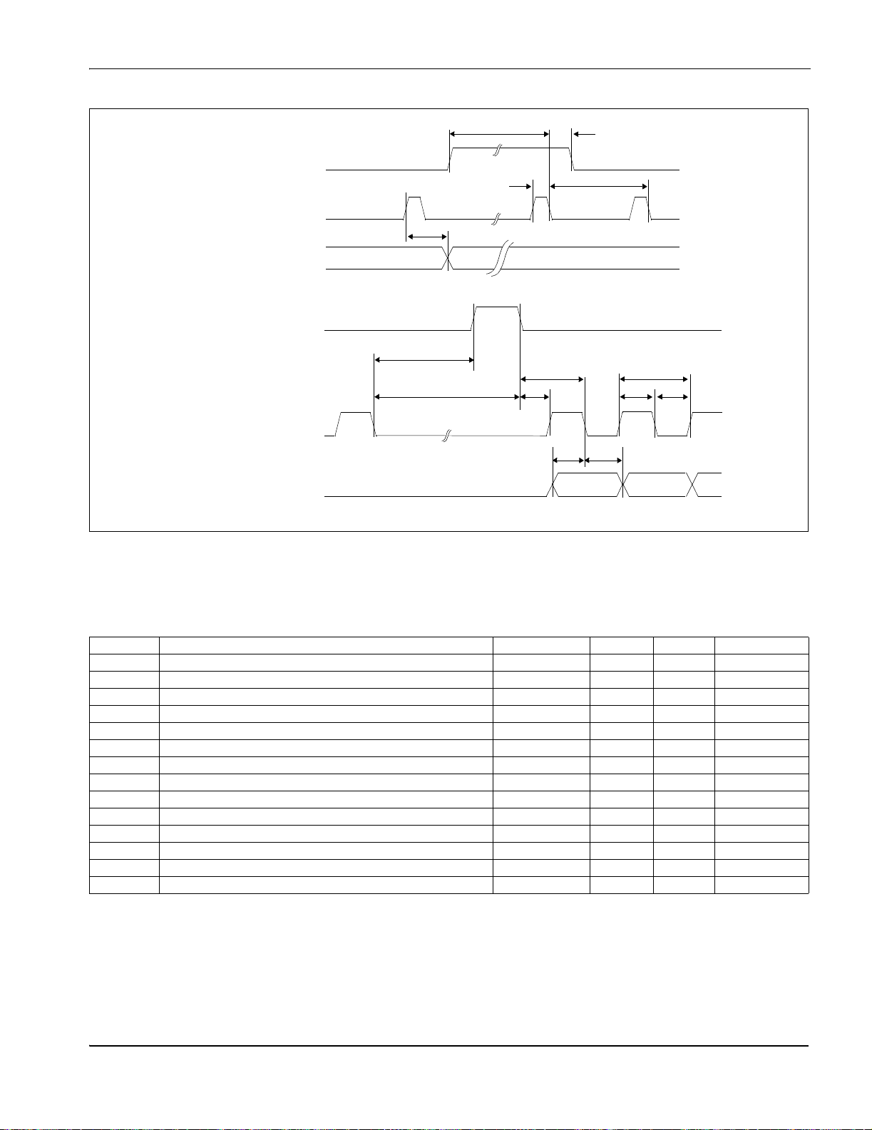
Table 7-11: Single Monochrome 4-Bit Panel A.C. Timing
Symbol Parameter Min Typ Max Units
t1 Frame Pulse setup to Line Pulse falling edge note 2 (note 1)
t2 Frame Pulse hold from Line Pulse falling edge 9 Ts
t3 Line Pulse period note 3
t4 Line Pulse pulse width 9 Ts
t5 MOD delay from Line Pu lse rising edge 1 Ts
t6 Shift Pulse falling edge to Line Pulse rising edge note 4
t7 Shift Pulse falling edge to Line Pulse falling edge note 5
t8 Line Pulse falling edge to Shift Pulse falling edge t14 + 2 Ts
t9 Shift Pulse period 4 Ts
t10 Shift Pulse pulse width low 2 Ts
t11 Shift Pulse pulse width high 2 Ts
t12 FPDAT[7:4] setup to Shift Pulse falling edge 2 Ts
t13 FPDAT[7:4] hold to Shift Pulse falling edge 2 Ts
t14 Line Pulse falling edge to Shift Pulse rising edge 23 Ts
1. Ts = pixel clock period
2. t1
3. t3
4. t6
5. t7
= t3
min
= [((REG[04h] bits 6-0)+1) x 8 + ((REG[08h] bits 4-0) + 4) x 8]Ts
min
= [(REG[08h] bits 4-0) x 8 + 2]Ts
min
= [(REG[08h] bits 4-0) x 8 + 11]Ts
min
min
- 9Ts
Hardware Functional Specification S1D13705
Issue Date: 02/02/01 X27A-A-001-10
Page 46

Page 40 Epson Research and Development
Vancouver Design Center
7.3.4 Single Monochrome 8-Bit Panel Timing
FPFRAME
FPLINE
DRDY (MOD)
FPDAT[7:0]
FPLINE
DRDY (MOD)
FPSHIFT
FPDAT7
FPDAT6
FPDAT5
FPDAT4
FPDAT3
FPDAT2
FPDAT1
FPDAT0
VDP
LINE1 LINE2 LINE3 LINE4 LINE479 LINE480
HDP
1-1 1-9
1-2 1-10 1-634
1-3
1-11
1-4 1-12
1-5 1-13
1-6 1-14
1-7 1-15 1-639
1-8 1-16
VNDP
1-633
1-635
1-636
1-637
1-638
1-640
LINE1 LINE2
HNDP
* Diagram drawn with 2 FPLINE vertical blank period
Example timing for a 640x480 panel
For this timing diagram Mask FPSHIFT, REG[01h] bit 3, is set to 1
Figure 7-13: Single Monochrome 8-Bit Panel Timing
VDP = Vertical Display Period = (REG[06h] bits 1-0, REG[05h] bits 7-0) + 1 Lines
VNDP = Vertical Non-Display Period = REG[0Ah] bits 5-0 Lines
HDP = Horizontal Display Period = ((REG[04h] bits 6-0) + 1) x 8Ts
HNDP = Horizontal Non-Display Period = (REG[08h] + 4) x 8Ts
S1D13705 Hardware Functional Specification
X27A-A-001-10 Issue Date: 02/02/01
Page 47
Epson Research and Development Page 41
Vancouver Design Center
Sync Timing
Frame Pulse
Line Pulse
t5
DRDY (MOD)
Data Timing
Line Pulse
t6
Shift Pulse
FPDAT[7:0]
Note: For this timing diagram Mask FPSHIFT, REG[01h] bit 3, is set to 1
t1
t7
t2
t4
t8 t9
t14
t3
t12 t13
12
t10t11
Figure 7-14: Single Monochrome 8-Bit Panel A.C. Timing
Table 7-12: Single Monochrome 8-Bit Panel A.C. Timing
Symbol Parameter Min Typ Max Units
t1 Frame Pulse setup to Line Pulse falling edge note 2 (note 1)
t2 Frame Pulse hold from Line Pulse falling edge 9 Ts
t3 Line Pulse period note 3
t4 Line Pulse pulse width 9 Ts
t5 MOD delay from Line Pulse rising edge 1 Ts
t6 Shift Pulse falling edge to Line Pulse rising edge note 4
t7 Shift Pulse falling edge to Line Pulse falling edge note 5
t8 Line Pulse falling edge to Shift Pulse falling edge t14 + 4 Ts
t9 Shift Pulse period 8 Ts
t10 Shift Pulse pulse width low 4 Ts
t11 Shift Pulse pulse width high 4 Ts
t12 FPDAT[7:0] setup to Shift Pulse falling edge 4 Ts
t13 FPDAT[7:0] hold to Shift Pulse falling edge 4 Ts
t14 Line Pulse falling edge to Shift Pulse rising edge 23 Ts
1. Ts = pixel clock period
2. t1
3. t3
4. t6
5. t7
= t3
min
= [((REG[04h] bits 6-0)+1) x 8 + ((REG[08h] bits 4-0) + 4) x 8]Ts
min
= [(REG[08h] bits 4-0) x 8 + 4]Ts
min
=[(REG[08h] bits 4-0) x 8 + 13]Ts
min
min
- 9Ts
Hardware Functional Specification S1D13705
Issue Date: 02/02/01 X27A-A-001-10
Page 48

Page 42 Epson Research and Development
Vancouver Design Center
7.3.5 Single Color 4-Bit Panel Timing
FPFRAME
FPLINE
DRDY (MOD)
FPDAT[7:4]
FPLINE
DRDY (MOD)
FPSHIFT
FPDAT7
FPDAT6
FPDAT5
FPDAT4
* Diagram drawn with 2 FPLINE vertical blank period
Example timing for a 320x240 panel
1-R1
1-G1
1-B1
1-R2
VDP
LINE1 LINE2 LINE3 LINE4
1-G2
1-B3
1-B2
1-R4
1-R3
1-G4
1-G3
1-B4
HDP
LINE239 LINE240
VNDP
LINE1 LINE2
HNDP
1-B319
1-R320
1-G320
1-B320
Figure 7-15: Single Color 4-Bit Panel Timing
VDP = Vertical Display Period = (REG[06h] bits 1-0, REG[05h] bits 7-0) + 1 Lines
VNDP = Vertical Non-Display Period = REG[0Ah] bits 5-0 Lines
HDP = Horizontal Display Period = ((REG[04h] bits 6-0) + 1) x 8Ts
HNDP = Horizontal Non-Display Period = (REG[08h] + 4) x 8Ts
S1D13705 Hardware Functional Specification
X27A-A-001-10 Issue Date: 02/02/01
Page 49

Epson Research and Development Page 43
Vancouver Design Center
Sync Timing
Data Timing
Frame Pulse
Line Pulse
DRDY (MOD)
Line Pulse
Shift Pulse
FPDAT[7:4]
t1
t5
t6
t7
t2
t4
t8 t9
t14
t3
t12 t13
12
t10t11
Figure 7-16: Single Color 4-Bit Panel A.C. Timing
Table 7-13: Single Color 4-Bit Panel A.C. Timing
Symbol Parameter Min Typ Max Units
t1 Frame Pulse setup to Line Pulse falling edge note 2 (note 1)
t2 Frame Pulse hold from Line Pulse falling edge 9 Ts
t3 Line Pulse period note 3
t4 Line Pulse pulse width 9 Ts
t5 MOD delay from Line Pulse rising edge 1 Ts
t6 Shift Pulse falling edge to Line Pulse rising edge note 4
t7 Shift Pulse falling edge to Line Pulse falling edge note 5
t8 Line Pulse falling edge to Shift Pulse falling edge t14 + 0.5 Ts
t9 Shift Pulse period 1 Ts
t10 Shift Pulse pulse width low 0.5 Ts
t11 Shift Pulse pulse width high 0.5 Ts
t12 FPDAT[7:4] setup to Shift Pulse falling edge 0.5 Ts
t13 FPDAT[7:4] hold to Shift Pulse falling edge 0.5 Ts
t14 Line Pulse falling edge to Shift Pulse rising edge 24 Ts
1. Ts = pixel clock period
2. t1
3. t3
4. t6
5. t7
= t3
min
= [((REG[04h] bits 6-0)+1) x 8 + ((REG[08h] bits 4-0) + 4) x 8]Ts
min
= [(REG[08h] bits 4-0) x 8 + 1.5]Ts
min
= [(REG[08h] bits 4-0) x 8 + 10]Ts
min
min
- 9Ts
Hardware Functional Specification S1D13705
Issue Date: 02/02/01 X27A-A-001-10
Page 50

Page 44 Epson Research and Development
Vancouver Design Center
7.3.6 Single Color 8-Bit Panel Timing (Format 1)
FPFRAME
FPLINE
FPDAT[7:0]
FPLINE
FPSHIFT
FPSHIFT 2
FPDAT7
FPDAT6
FPDAT5
FPDAT4
FPDAT3
FPDAT2
FPDAT1
FPDAT0
LINE1 LINE2 LINE3 LINE4
1-R1
1-G1
1-G6
1-B6
1-B1
1-R2
1-R7
1-G7
1-G2
1-B2
1-B7
1-R8
1-R3
1-G3
1-G8
1-B8
1-B3
1-R4
1-R9
1-G9
1-G4
1-B4
1-B9
1-R10
1-R5
1-G5
1-G10
1-B10
1-B5
1-R6
1-R11
1-G11
1-B11
1-G12
1-R13
1-B13
1-G14
1-R15
1-B15
1-G16
VDP
HDP
1-R12
1-B12
1-G13
1-R14
1-B14
1-G15
1-R16
1-B16
LINE479 LINE480
VNDP
LINE1 LINE2
HNDP
1-R636
1-B636
1-G637
1-R638
1-B638
1-G639
1-R640
1-B640
* Diagram drawn with 2 FPLINE vertical blank period
Example timing for a 640x480 panel
Figure 7-17: Single Color 8-Bit Panel Timing (Format 1)
VDP = Vertical Display Period = (REG[06h] bits 1-0, REG[05h] bits 7-0) + 1 Lines
VNDP = Vertical Non-Display Period = REG[0Ah] bits 5-0 Lines
HDP = Horizontal Display Period = ((REG[04h] bits 6-0) + 1) x 8Ts
HNDP = Horizontal Non-Display Period = (REG[08h] + 4) x 8Ts
S1D13705 Hardware Functional Specification
X27A-A-001-10 Issue Date: 02/02/01
Page 51

Epson Research and Development Page 45
Vancouver Design Center
Sync Timing
Data Timing
t1
Frame Pulse
t4
Line Pulse
Line Pulse
t6a
t6b
t7a
Shift Pu lse 2
t7b
Shift Pulse
FPDAT[7:0]
t2
t3
t8 t9
t14
t12
t12 t13
t13
12
Figure 7-18: Single Color 8-Bit Panel A.C. Timing (Format 1)
t10t11
Table 7-14: Single Color 8-Bit Panel A.C. Timing (Format 1)
Symbol Parameter Min Typ Max Units
t1 Frame Pulse setup to Line Pulse falling edge note 2 (note 1)
t2 Frame Pulse hold from Line Pulse falling edge 9 Ts
t3 Line Pulse period note 3
t4 Line Pulse pulse width 9 Ts
t6a Shift Pulse falling edge to Line Pulse rising edge note 4
t6b Shift Pulse 2 falling edge to Line Pulse rising edge note 5
t7a Shift Pulse 2 falling edge to Line Pulse falling edge note 6
t7b Shift Pulse falling edge to Line Pulse falling edge note 7
t8 Line Pulse falling edge to Shift Pulse rising, Shift Pulse 2 falling edge t14 + 2 Ts
t9 Shift Pulse 2, Shift Pulse period 4 Ts
t10 Shift Pulse 2, Shift Pulse pulse width low 2 Ts
t11 Shift Pulse 2, Shift Pulse pulse width high 2 Ts
t12 FPDAT[7:0] setup to Shift Pulse 2, Shift Pulse falling edge 1 Ts
t13 FPDAT[7:0] hold from Shift Pulse 2, Shift Pulse falling edge 1 Ts
t14 Line Pulse falling edge to Shift Pulse rising edge 25 Ts
1. Ts = pixel clock period
2. t1
3. t3
4. t6a
5. t6b
6. t7a
7. t7b
= t3
min
= [((REG[04h] bits 6-0)+1) x 8 + ((REG[08h] bits 4-0) + 4) x 8]Ts
min
= [(REG[08h] bits 4-0) x 8]Ts
min
= [(REG[08h] bits 4-0) x 8 + 2]Ts
min
= [(REG[08h] bits 4-0) x 8 + 11]Ts
min
= [(REG[08h] bits 4-0) x 8 + 11] - t10]Ts
min
min
- 9Ts
Hardware Functional Specification S1D13705
Issue Date: 02/02/01 X27A-A-001-10
Page 52

Page 46 Epson Research and Development
Vancouver Design Center
7.3.7 Single Color 8-Bit Panel Timing (Format 2)
FPFRAME
FPLINE
DRDY (MOD)
FPDAT[7:0]
FPLINE
DRDY (MOD)
FPSHIFT
FPDAT7
FPDAT6
FPDAT5
FPDAT4
FPDAT3
FPDAT2
FPDAT1
FPDAT0
VDP
LINE1 LINE2 LINE3 LINE4 LINE479 LINE480
HDP
1-R1
1-B3
1-G6
1-G 1
1-R4
1-B6
1-B1
1-G 4
1-R7
1-R2
1-B4
1-G7
1-G 2
1-R5
1-B7
1-B2
1-G5
1-R8
1-R3
1-B5
1-G8
1-G 3
1-R6
1-B8
VNDP
LINE1 LINE2
HNDP
1-G638
1-B638
1-R639
1-G639
1-B639
1-R640
1-G640
1-B640
* Diagram drawn with 2 FPLINE vertical blank period
Example timing for a 640x480 panel
Figure 7-19: Single Color 8-Bit Panel Timing (Format 2)
VDP = Vertical Display Period = (REG[06h] bits 1-0, REG[05h] bits 7-0) + 1 Lines
VNDP = Vertical Non-Display Period = REG[0Ah] bits 5-0 Lines
HDP = Horizontal Display Period = ((REG[04h] bits 6-0) + 1) x 8Ts
HNDP = Horizontal Non-Display Period = (REG[08h] + 4) x 8Ts
S1D13705 Hardware Functional Specification
X27A-A-001-10 Issue Date: 02/02/01
Page 53

Epson Research and Development Page 47
Vancouver Design Center
Sync Timing
Data Timing
t1
Frame Pulse
Line Pulse
t5
DRDY (MOD)
Line Pulse
t6
t7
Shift Pulse
FPDAT[7:0]
t2
t4
t8 t9
t14 t10t11
t3
t12 t13
12
Figure 7-20: Single Color 8-Bit Panel A.C. Timing (Format 2)
Table 7-15: Single Color 8-Bit Panel A.C. Timing (Format 2)
Symbol Parameter Min Typ Max Units
t1 Frame Pulse setup to Line Pulse falling edge note 2 (note 1)
t2 Frame Pulse hold from Line Pulse falling edge 9 Ts
t3 Line Pulse period note 3
t4 Line Pulse pulse width 9 Ts
t5 MOD delay from Line Pulse rising edge 1 Ts
t6 Shift Pulse falling edge to Line Pulse rising edge note 4
t7 Shift Pulse falling edge to Line Pulse falling edge note 5
t8 Line Pulse falling edge to Shift Pulse falling edge t14 + 2 Ts
t9 Shift Pulse period 2 Ts
t10 Shift Pulse pulse width low 1 Ts
t11 Shift Pulse pulse width high 1 Ts
t12 FPDAT[7:0] setup to Shift Pulse falling edge 1 Ts
t13 FPDAT[7:0] hold to Shift Pulse falling edge 1 Ts
t14 Line Pulse falling edge to Shift Pulse rising edge 23 Ts
1. Ts = pixel clock period
2. t1
3. t3
4. t6
5. t7
= t3
min
= [((REG[04h] bits 6-0)+1) x 8 + ((REG[08h] bits 4-0) + 4) x 8]Ts
min
= [(REG[08h] bits 4-0) x 8 + 1]Ts
min
= [(REG[08h] bits 4-0) x 8 + 10]Ts
min
min
- 9Ts
Hardware Functional Specification S1D13705
Issue Date: 02/02/01 X27A-A-001-10
Page 54

Page 48 Epson Research and Development
Vancouver Design Center
7.3.8 Dual Monochrome 8-Bit Panel Timing
FPFRAME
FPLINE
DRDY (MOD)
FPDAT[7:0]
FPLINE
DRDY (MOD)
FPSHIFT
FPDAT7
FPDAT6
FPDAT5
FPDAT4
FPDAT3
FPDAT2
FPDAT1
FPDAT0
VDP
LINE 1/241 LINE 2/242 LINE 3/243 LINE 4/244 LINE 239/479 LINE 240/480 LINE 1/241 LINE 2/242
HDP
1-1 1-5
1-2 1-6 1-638
1-3
1-7
1-4 1-8
241-1 241-5
241-2 241-6
241-3 241-7
241-4 241-8
VNDP
HNDP
1-637
1-639
1-640
241-637
241-638
241-639
241-640
* Diagram drawn with 2 FPLINE vertical blank period
Example timing for a 640x480 panel
Figure 7-21: Dual Monochrome 8-Bit Panel Timing
VDP = Vertical Display Period = (REG[06h] bits 1-0, REG[05h] bits 7-0) + 1 Lines
VNDP = Vertical Non-Display Period = REG[0Ah] bits 5-0 Lines
HDP = Horizontal Display Period = ((REG[04h] bits 6-0) + 1) x 8Ts
HNDP = Horizontal Non-Display Period = (REG[08h] + 4) x 8Ts
S1D13705 Hardware Functional Specification
X27A-A-001-10 Issue Date: 02/02/01
Page 55

Epson Research and Development Page 49
Vancouver Design Center
Sync Timing
Frame Pulse
Line Pulse
t5
DRDY (MOD)
Data Timing
Line Pulse
t6
Shift Pulse
FPDAT[7:0]
Note: For this timing diagram Mask FPSHIFT, REG[01h] bit 3, is set to 1
t1 t2
t4
t8 t9
t7
t14 t10t11
t3
t12 t13
12
Figure 7-22: Dual Monochrome 8-Bit Panel A.C. Timing
Table 7-16: Dual Monochrome 8-Bit Panel A.C. Timing
Symbol Parameter Min Typ Max Units
t1 Frame Pulse setup to Line Pulse falling edge note 2 (note 1)
t2 Frame Pulse hold from Line Pulse falling edge 9 Ts
t3 Line Pulse period note 3
t4 Line Pulse pulse width 9 Ts
t5 MOD delay from Line Pulse falling edge 1 Ts
t6 Shift Pulse falling edge to Line Pulse rising edge note 5
t7 Shift Pulse falling edge to Line Pulse falling edge note 6
t8 Line Pulse falling edge to Shift Pulse falling edge t14 + 2 Ts
t9 Shift Pulse period 8 Ts
t10 Shift Pulse pulse width low 4 Ts
t11 Shift Pulse pulse width high 4 Ts
t12 FPDAT[7:0] setup to Shift Pulse falling edge 4 Ts
t13 FPDAT[7:0] hold to Shift Pulse falling edge 4 Ts
t14 Line Pulse falling edge to Shift Pulse rising edge 39 Ts
1. Ts = pixel clock period
2. t1
3. t3
5. t6
6. t7
= t3
min
= [(((REG[04h] bits 6-0)+1) x 8 + ((REG[08h] bits 4-0) + 4) x 8) x 2]Ts
min
= [((REG[08h] bits 4-0) x 2)x 8 + 20]Ts
min
= [((REG[08h] bits 4-0) x 2)x 8 + 29]Ts
min
min
- 9Ts
Hardware Functional Specification S1D13705
Issue Date: 02/02/01 X27A-A-001-10
Page 56

Page 50 Epson Research and Development
Vancouver Design Center
7.3.9 Dual Color 8-Bit Panel Timing
FPFRAME
FPLINE
DRDY (MOD)
FPDAT[7:0]
FPLINE
DRDY (MOD)
FPSHIFT
FPDAT7
FPDAT6
FPDAT5
FPDAT4
FPDAT3
FPDAT2
FPDAT1
FPDAT0
VDP
LINE 1/241 LINE 2/242 LINE 239/479 LINE 240/480 LIN E 1/241
VNDP
HDP
1-R1
1-G1
1-B1
1-R2
241-R1
241-G1
241-B1
241-R2
1-G2
1-B2
1-R3
1-G3
241-G2
241-B2
241-R3
241-G3
1-B3
1-R4
1-G4
1-B4
241-B3
241-R4
241-G4
241-B4
1-R5
1-G5
1-B5
1-R6
241-R5
241-G5
241-B5
241-R6
1-G6
1-B6
1-R7
1-G7
241-G6
241-B6
241-R7
241-G7
1-B7
1-R8
1-G8
1-B8
241-B7
241-R8
241-G8
241-B8
1-B639
1-R640
1-G640
1-B640
241-
B639
241-
R640
241-
G640
241-
B640
HNDP
* Diagram drawn with 2 FPLINE vertical blank period
Example timing for a 640x480 panel
Figure 7-23: Dual Color 8-Bit Panel Timing
VDP = Vertical Display Period = (REG[06h] bits 1-0, REG[05h] bits 7-0) + 1 Lines
VNDP = Vertical Non-Display Period = REG[0Ah] bits 5-0 Lines
HDP = Horizontal Display Period = ((REG[04h] bits 6-0) + 1) x 8Ts
HNDP = Horizontal Non-Display Period = (REG[08h] + 4) x 8Ts
S1D13705 Hardware Functional Specification
X27A-A-001-10 Issue Date: 02/02/01
Page 57

Epson Research and Development Page 51
Vancouver Design Center
Sync Timing
Data Timing
Frame Pulse
Line Pulse
DRDY (MOD)
Line Pulse
Shift Pulse
FPDAT[7:0]
t1 t2
t4
t5
t6
t8 t9
t7
t14 t10t11
t3
t12 t13
12
Figure 7-24: Dual Color 8-Bit Panel A.C. Timing
Table 7-17: Dual Color 8-Bit Panel A.C. Timing
Symbol Parameter Min Typ Max Units
t1 Frame Pulse setup to Line Pulse falling edge note 2 (note 1)
t2 Frame Pulse hold from Line Pulse falling edge 9 Ts
t3 Line Pulse period note 3
t4 Line Pulse pulse width 9 Ts
t5 MOD delay from Line P ulse falling edge 1 Ts
t6 Shift Pulse falling edge to Line Pulse rising edge note 5
t7 Shift Pulse falling edge to Line Pulse falling edge note 6
t8 Line Pulse falling edge to Shift Pulse falling edge t14 + 1 Ts
t9 Shift Pulse period 2 Ts
t10 Shift Pulse pulse width low 1 Ts
t11 Shift Pulse pulse width high 1 Ts
t12 FPDAT[7:0] setup to Shift Pulse falling edge 1 Ts
t13 FPDAT[7:0] hold to Shift Pulse falling edge 1 Ts
t14 Line Pulse falling edge to Shift Pulse rising edge 39 Ts
1. Ts = pixel clock period
2. t1
3. t3
5. t6
6. t7
= t3
min
= [(((REG[04h] bits 6-0)+1) x 8 + ((REG[08h] bits 4-0) + 4) x 8) x 2]Ts
min
= [((REG[08h] bits 4-0) x 2)x 8 + 17]Ts
min
= [((REG[08h] bits 4-0) x 2)x 8 + 26]Ts
min
min
- 9Ts
Hardware Functional Specification S1D13705
Issue Date: 02/02/01 X27A-A-001-10
Page 58

Page 52 Epson Research and Development
Vancouver Design Center
7.3.10 9/12-Bit TFT/D-TFD Panel Timing
FPFRAME
FPLINE
FPDAT[11:0]
DRDY
FPLINE
FPSHIFT
DRDY
FPDAT[9]
FPDAT[2:0]
FPDAT[10]
FPDAT[4:3]
FPDAT[11]
FPDAT[8:6]
LINE480
HNDP
VNDP
2
2
1-1
1-2
1-1
1-2
1-1
1-2
VDP
LINE1 LINE480
HDP
1-640
1-640
1-640
HNDP
VNDP
1
1
Note: DRDY is used to indicate the first pixel
Example Timing for 12-bit 640x480 panel
Figure 7-25: 12-Bit TFT/D-TFD Panel Timing
VDP = Vertical Display Period = (REG[06h] bits 1-0, REG[05h] bits 7-0) + 1 Lines
VNDP = Vertical Non-Display Period = VNDP1 + VNDP2 = (REG[0Ah] bits 5-0) Lines
VNDP1 = Vertical Non-Disp la y Per io d 1 = REG[09h] bits 5-0 Lines
VNDP2 = Vertical Non-Disp lay Period 2 = (R EG[0A h] bits 5-0 ) - (REG[09A h] bit s 5-0 ) Lines
HDP = Horizontal Display Period = ((REG[04h] bits 6-0) + 1) x 8Ts
HNDP = Horizontal Non-Display Period = HNDP1 + HNDP2 = (REG[08h] + 4) x 8Ts
HNDP1= Horizontal Non-Display Period 1 = ((REG[07h] bits4-0) x 8) +16Ts
HNDP2= Horizontal Non-Display Period 2 = (((REG[08h] bits4-0) - (REG[07h] bits 4-0)) x 8) +16Ts
S1D13705 Hardware Functional Specification
X27A-A-001-10 Issue Date: 02/02/01
Page 59

Epson Research and Development Page 53
Vancouver Design Center
t8
t9
Frame Pulse
t12
Line Pulse
t6
Line Pulse
DRDY
t1
t3
t2
t11
Shift Pulse
FPDAT[11:0]
Note: DRDY is used to indicate the first pixel
t7
t17
Figure 7-26: TFT/D-TFD A.C. Timing
t13
t4
t14
t5
21639
t10
t15
t16
640
Hardware Functional Specification S1D13705
Issue Date: 02/02/01 X27A-A-001-10
Page 60

Page 54 Epson Research and Development
Vancouver Design Center
Table 7-18: TFT/D-TFD A.C. Timing
Symbol Parameter Min Typ Max Units
t1
t2
t3
t4
t5
t6
t7
t8 Frame Pulse cycle time note 3
t9 Frame Pulse pulse width low 2t6
t10 horizontal display period note 4
t11 Line Pulse setup to Shift Pulse falling edge 0.5 Ts
t12
t13 DRDY to Shift Pulse falling edge setup time 0.5 Ts
t14 DRDY pulse width note 5
t15 DRDY falling edge to Line Pulse falling edge note 6
t16 DRDY hold from Shift Pulse falling edge 0.5 Ts
t17 Line Pulse Falling edge to DRDY active note 7 250
Shift Pulse period 1 (note 1)
Shift Pulse pulse width high 0.5 Ts
Shift Pulse pulse width low 0.5 Ts
data setup to Shift Pulse falling edge 0.5 Ts
data hold from Shift Pulse falling edge 0.5 Ts
Line Pulse cycle time note 2
Line Pulse pulse width low 9 Ts
Frame Pulse falling edge to Line Pulse falling
edge phase difference
t6 - 18Ts
1. Ts = pixel clock period
2. t6min = [((REG[04h] bits 6-0)+1) x 8 + ((REG[08h] bits 4-0)+4) x 8] Ts
3. t8 min = [((REG[06h] bits 1-0, REG[05h] bits 7-0)+1) + (REG[0Ah] bits 6-0)] Lines
4. t10min = [((REG[04h] bits 6-0)+1) x 8] Ts
5. t14min = [((REG[04h] bits 6-0)+1) x 8] Ts
6. t15min = [(REG[07h] bits 4-0) x 8 + 16] Ts
7. t17min = [(REG[08h] bits 4-0) - (REG[07]) x 8 + 16] Ts
S1D13705 Hardware Functional Specification
X27A-A-001-10 Issue Date: 02/02/01
Page 61

Epson Research and Development Page 55
Vancouver Design Center
8 Registers
8.1 Register Mapping
The S1D13705 registers are located in the upper 32 bytes of the 128K byte S1D13705
address range. The registers are accessible when CS# = 0 and AB[16:0] are in the range
1FFE0h through 1FFFFh.
8.2 Register Descriptions
Unless specified otherwise, all register bits are reset to 0 during power up.
All bits marked n/a should be programmed 0.
REG[00h] Revision Code Register
Address = 1FFE0h Read Only.
Product Code
Bit 5
Product Code
Bit 4
Product Code
Bit 3
Product Code
Bit 2
Product Code
Bit 1
Product Code
Bit 0
Revision
Code Bit 1
Revision
Code Bit 0
bits 7-2 Product Code
This is a read-only re gi ster tha t indicat es th e pr oduct c ode of t he chip. The pr oduct code is
001001.
bits 1-0 Revision Code
This is a read -only re gist er that indica tes the re vision code of the chip. The re visio n code i s
00.
REG[01h] Mode Register 0
Address = 1FFE1h Read/Write.
TFT/STN Dual/Single Color/Mono
FPLine
Polarity
FPFrame
Polarity
Mask
FPSHIFT
Data Width
Bit 1
Data Width
Bit 0
bit 7 TFT/STN
When this bit = 0, STN (passive) panel mode is selected. When this bit = 1, TFT/D-TFD
panel mode is selecte d. If TFT/ D-TFD pane l mode is sele cted, Dua l/Sin gle (REG[ 01h] bi t
6) and Color/Mono (REG[01h] bit5) are ignored. See Table 8-1: “ Panel Dat a Format” for a
comprehensive description of panel selection.
bit 6 Dual/Single
When this bit = 0, Single LCD panel drive is selected. When this bit = 1, Dual LCD panel
drive is selected. See Table 8-1: “Panel Data Format” for a comprehensive description of
panel selection.
bit 5 Color/Mono
When this bit = 0, Monochrome LCD panel drive is selected. When this bit = 1, Color
LCD panel d rive is selected. Se e Table 8-1: “Pane l Data Format” for a comprehensive
description of panel selection.
Hardware Functional Specification S1D13705
Issue Date: 02/02/01 X27A-A-001-10
Page 62

Page 56 Epson Research and Development
Vancouver Design Center
bit 4 FPLINE Polarity
This bit controls the polarity of FPLINE in TFT/D-TFD mode (no effect in passive panel
mode). When this bit = 0, FP LINE i s active low. When this bit = 1, FPLI NE is act i v e hig h.
bit 3 FPFRAME Polarity
This bit controls the polarity of FPFRAME in TFT/D-TFD mode (no effect in passive
panel mode). When this bit = 0, FPFRAME is active low. When this bit = 1, FPFRAME is
active high.
bit 2 Mask FPSHIFT
FPSHIFT is masked during non-display periods if either of the following two criteria is
met:
1. Color passive panel is selected (REG[01h] bit 5 = 1)
2. This bit (REG[01h] bit 2) = 1
bits 1-0 Data Width Bits [1:0 ]
These bits select the display data format. See Table 8-1: “Panel Data Format” below for a
comprehensive description of panel selection.
Table 8-1: Panel Data Format
TFT/STN
REG[01h] bit 7
0
1 X (don’t care)
Color/Mono
REG[01h] bit 5
0
1
Dual/Single
REG[01h] bit 6
Data Width
Bit 1
REG[01h] bit 1
0
0
1
0
1
1
0
0
1
0
1
1
Data Width
Bit 0
REG[01h] bit 0
0 Mono Single 4-bit passive LCD
1 Mono Single 8-bit passive LCD
0 reserved
1 reserved
0 reserved
1 Mono Dual 8-bit passive LCD
0 reserved
1 reserved
0 Color Single 4-bit passive LCD
1 Color Single 8-bit passive LCD format 1
0 reserved
1 Color Single 8-bit passive LCD format 2
0 reserved
1 Color Dual 8-bit passive LCD
0 reserved
1 reserved
0 9-bit TFT/D-TFD panel
1 12-bit TFT/D-TFD panel
Function
S1D13705 Hardware Functional Specification
X27A-A-001-10 Issue Date: 02/02/01
Page 63

Epson Research and Development Page 57
Vancouver Design Center
REG[02h] Mode Register 1
Address = 1FFE2h Read/Write.
Bit-Per-Pixel
Bit 1
Bit-Per-Pixel
Bit 0
High
Performance
Input Clock
divide
(CLKI/2)
Display Blank
Frame
Repeat
Hardware
Video Invert
Enable
Software
Video Invert
bits 7-6 Bit-Per-Pixel B i ts [1:0]
These bits select the color or gray-scale depth ( Display Mode).
Table 8-2: Gray Scale/Color Mode Selection
Color/Mono
REG[01h] bit 5
0
1
Bit-Per-Pixel Bit 1
REG[02h] bit 7
0
1
0
1
Bit-Per-Pixel Bit 0
REG[02h] bit 6
bit 5 High Performance (Landscape Modes Only)
When this bit = 0, the internal Memory Clock (MCLK) is a divided-down version of the
Pixel Clock (PCLK). The denominator is dependent on the bit-per-pixel mode - see the
table below.
Table 8-3: High Performance Selection
High Performance BPP Bit 1 BPP Bit 0 Display Modes
0
0
1
1XXMClk = PClk
Display Mode
0 2 Gray scale 1 bit-per-pixel
1 4 Gray scale 2 bit-per-pixel
0 16 Gray scale 4 bit-per-pixel
1reserved
0 2 Colors 1 bit-per-pixel
1 4 Colors 2 bit-per-pixel
0 16 Colors 4 bit-per-pixel
1 256 Colors 8 bit-per-pixel
0 MClk = PClk /8 1 bit-per-pixel
1 MClk = PClk /4 2 bit-per-pixel
0 MClk = PClk /2 4 bit-per-pixel
1 MClk = PClk 8 bit-per-pixel
When this bit = 1, MCLK is fixed to the same frequency as PCLK for all bit-per-pixel
modes. This provi des a faster screen update perfor mance i n 1/ 2/4 bi t- per-pixel modes, b ut
also increases power consumption. This bit can be set to 1 just before a major screen
update, then set back to 0 to save power after the update. This bit has no effect in SwivelView mode. Refer to REG[1Bh] SwivelView Mode Register on page 67 for SwivelView
mode clock selection.
Hardware Functional Specification S1D13705
Issue Date: 02/02/01 X27A-A-001-10
Page 64

Page 58 Epson Research and Development
Vancouver Design Center
bit 4 Input Clock Divide
When this bit = 0, the Operating Clock(CLK) is the same as the Input Clock (CLKI).
When this bit = 1, CLK = CLKI/2.
In landscape mode PCLK=CLK and MCLK is selected as per Table 8-3: “High Performance Selection”.
In SwivelView mode, MCLK and PCLK are derived from CLK as shown in Table 8-8:
“Selection of PCLK and MCLK in SwivelView Mode,” on page 68.
bit 3 Display Blank
This bit blanks the display image. When this bit = 1, the display is blanked (FPDAT lines
to the panel are driven low). When this bit = 0, the display is enabled.
bit 2 Frame Repeat (EL support)
This feature is used to improve Frame Rate Modulation of EL panels. When this bit = 1,
an internal frame counter runs from 0 to 3FFFFh. When the frame counter rolls over, the
modulated image pattern is repeated (every 1 hour when the frame rate is 72Hz). When
this bit = 0, the modulated image pattern is never repeated.
bit 1 Hardware Video Invert Enable
In passive panel modes (REG[01h] bit 7 = 0) FPDAT11 is available as either GPIO4 or
hardware video invert. When this bit = 1, Hardware Video Invert is enabled via the
FPDAT11 pin. When this bit = 0, FPDAT11 operates as GPIO4. See Table 8-4: “Inverse
Video Mode Select Options” below.
Note
Video data is inverted after the Look-Up Table.
bit 0 Software Video Invert
When this bit = 1, Inverse Video Mode is selected. When this bit = 0, Standard Video
Mode is selected. See Table 8-4: “Inverse Video Mode Select Options” below.
Note
Video data is inverted after the Look-Up Table.
Table 8-4: Inverse Video Mode Select Options
Hardware Video
Invert Enable
00 XNormal
01 XInverse
1X 0Normal
1X 1Inverse
Software Video Invert
(Passive and Active
Panels)
FPDAT11
(Passive Panels Only)
Video Data
S1D13705 Hardware Functional Specification
X27A-A-001-10 Issue Date: 02/02/01
Page 65

Epson Research and Development Page 59
Vancouver Design Center
REG[03h] Mode Register 2
Address = 1FFE3h Read/Write
n/an/an/an/a
LCDPWR
Override
Hardware
Power Save
Enable
Software
Power Save
Bit 1
Software
Power Save
Bit 0
bit 3 LCDPWR Override
This bit is used to ov erri de the pan el on/of f s equencing logic. Wh en this b it = 0, LCDPWR
and the panel interface signals are controlled by the sequencing logic. When this bit 1,
LCDPWR is forced to off and the panel interface signals are forced low immediately upon
entering power save mode. See Section 7.3.2, “Power Down/Up Timing” on page 37 for
further information.
bit 2 Hardware Power Save Enable
When this bit = 1 GPIO0 is used a s the Hardw are Power Save inpu t pin. When this bit = 0,
GPIO0 operates normally.
Table 8-5: Hardware Power Save/GPIO0 Operation
RESET#
State
Hardware Power
Save Enable
REG[03h] bit 2
0X X X
1 0 0 reads pin status
1 0 1 0 G PIO0 Output = 0
1 0 1 1 G PIO0 Output = 1
11 X X
bits 1-0 Software Power Save Bits [1: 0]
These bits select the Power Save Mode as shown in the following table.
Table 8-6: Software Power Save Mode Selection
Bit 1 Bit 0 Mode
0 0 Software Power Save
0 1 reserved
1 0 reserved
1 1 Normal Operation
GPIO0 Config
REG[18h] bit 0
GPIO0
Status/Control
REG[19h] bit 0
GPIO0 Operation
GPIO0 Input
(high impedance)
Hardware Power Save
Input (active high)
Refer to Section 13, “Power Save Modes” on page 82 for a complete description of the
power save modes.
Hardware Functional Specification S1D13705
Issue Date: 02/02/01 X27A-A-001-10
Page 66

Page 60 Epson Research and Development
Vancouver Design Center
REG[04h] Horizontal Panel Size Register
Address = 1FFE4h Read/Write
n/a
Horizontal
Panel Size Bit
6
Horizontal
Panel Size Bit
5
Horizontal
Panel Size Bit
4
Horizontal
Panel Size Bit
3
Horizontal
Panel Size Bit
2
Horizontal
Panel Size Bit
1
Horizontal
Panel Size Bit
0
bits 6-0 Horizontal Panel Size Bits [6:0]
This register determines the horizontal resolution of the panel. This register must be programmed w ith a value calculated as follows:
HorizontalPanelSizeRegister
----------------------------------------------------------------------------------------------
8
1–=
HorizontalPanelResolution pixels()
Note
This register must not be set to a value less than 03h.
REG[05h] Vertical Panel Size Register (LSB)
Address = 1FFE5h Read/Write
Vertical Panel
Size
Bit 7
Vertical Panel
Size
Bit 6
Vertical Panel
Size
Bit 5
Vertical Panel
Size
Bit 4
Vertical Panel
Size
Bit 3
Vertical Panel
Size
Bit 2
Vertical Panel
Size
Bit 1
Vertical Panel
Size
Bit 0
.
REG[06h] Vertical Panel Size Register (MSB)
Address = 1FFE6h Read/Write
n/a n/a n/a n /a n/a n/a
Vertical Panel
Size
Bit 9
Vertical Panel
Size
Bit 8
REG[05h] bits 7-0 Vertical Panel Size Bits [9:0]
REG[06h] bits 1-0 This 10-bit register determines the vertical resolution of the panel. This register must be
programmed with a value calculated as follows:
VerticalPanelSizeRegister VerticalPanelResolution lines()1–=
3FFh is the maximum value of this register for a vertical resolution of 1024 lines.
S1D13705 Hardware Functional Specification
X27A-A-001-10 Issue Date: 02/02/01
Page 67

Epson Research and Development Page 61
Vancouver Design Center
REG[07h] FPLINE Start Position
Address = 1FFE7h Read/Write
n/a n/a n/a
FPLINE Start
Position Bit 4
FPLINE Start
Position Bit 3
FPLINE Start
Position Bit 2
FPLINE Start
Position Bit 1
FPLINE Start
Position Bit 0
bits 4-0 FPLINE Start Position
These bits are used in TFT/D-TFD mode to specify the position of the FPLINE pulse.
These bits specify the delay, in 8-pixel resolution, from the end of a line of display data
(FPDAT) to the leading edge of FPLINE. This register is effective in TFT/D-TFD mode
only (REG[01h] bit 7 = 1). This register is programmed as follows:
FPLINEposition pixels()REG 07h[]2+()8×=
The following constraint must be satisfied:
REG 07h[]REG 08h[]≤
REG[08h] Horizontal Non-Display Period
Address = 1FFE8h Read/Write
n/a n/a n/a
Horizontal
Non-Display
Period Bit 4
Horizontal
Non-Display
Period Bit 3
Horizontal
Non-Display
Period Bit 2
Horizontal
Non-Display
Period Bit 1
Horizontal
Non-Display
Period Bit 0
bits 4-0 Horizontal Non-Display Period
These bits specify the horizontal non-display period in 8-pixel resolution.
HorizontalNonDisplayPeriod pixels()REG 08h[]4+()8×=
REG[09h] FPFRAME Start Position
Address = 1FFE9h Read/Write
n/a n/a
FPFRAME
Start Position
Bit 5
FPFRAME
Start Position
Bit 4
FPFRAME
Start Position
Bit 3
FPFRAME
Start Position
Bit 2
FPFRAME
Start Position
Bit 1
FPFRAME
Start Position
Bit 0
bits 5-0 FPFRAME Start Position
These bits are used in TFT/D-TFD mode to specify the position of the FPFRAME pulse.
These bits specify the number of lines between the last line of display data (FPDAT) and
the leading edge of FPFRAME. This register is effective in TFT/D-TFD mode only
(REG[01h] bit 7 = 1). This register is programmed as follows:
FPFRAMEposition lines()REG 09h[]=
The contents of this register must be greater than zero and less than or equal to the Vertical
Non-Display Period Register, i.e.
1REG09h[]REG 0Ah[]Bits 5:0≤≤
Hardware Functional Specification S1D13705
Issue Date: 02/02/01 X27A-A-001-10
Page 68

Page 62 Epson Research and Development
Vancouver Design Center
REG[0Ah] Vertical Non-Display Period
Address = 1FFEAh Read/Write
Vertical Non-
Display
Status
n/a
Vertical Non-
Display
Period Bit 5
Vertical Non-
Display
Period Bit 4
Vertical Non-
Display
Period Bit 3
Vertical Non-
Display
Period Bit 2
Vertical Non-
Display
Period Bit 1
Vertical Non-
Display
Period Bit 0
bit 7 Vertical Non-Display Status
This bit =1 during the Vertical Non-Display period.
bits 5-0 Vertical Non-Display Period
These bits specify the v e rt ic al non-display period. This register is pr ogr amme d as fo ll ows:
VerticalNonDisplayPeriod lines()REG[0Ah] bits [5:0]=
Note
This register should be set only once, on power-up during initialization.
.
REG[0Bh] MOD Rate Register
Address = 1FFEBh Read/Write
n/a n/a
MOD Rate
Bit 5
MOD Rate
Bit 4
MOD Rate
Bit 3
MOD Rate
Bit 2
MOD Rate
Bit 1
MOD Rate
Bit 0
bits 5-0 MOD Rate Bits [5:0]
When the value o f t his register is 0, the MOD output signal t oggl es every FPFRAME. For
a non-zero value, the value in this register + 1 specifies the number of FPLINEs between
toggles of the MOD output signal. These bits are for passive LCD panels only.
S1D13705 Hardware Functional Specification
X27A-A-001-10 Issue Date: 02/02/01
Page 69

Epson Research and Development Page 63
Vancouver Design Center
REG[0Ch] Screen 1 Start Address Register (LSB)
Address = 1FFECh Read/Write
Screen 1 Start
Address
Bit 7
Screen 1 Start
Address
Bit 6
Screen 1 Start
Address
Bit 5
Screen 1 Start
Address
Bit 4
Screen 1 Start
Address
Bit 3
Screen 1 Start
Address
Bit 2
Screen 1 Start
Address
Bit 1
Screen 1 Start
Address
Bit 0
REG[0Dh] Screen 1 Start Address Register (MSB)
Address = 1FFEDh Read/Write
Screen 1 Start
Address
Bit 15
Screen 1 Start
Address
Bit 14
Screen 1 Start
Address
Bit 13
Screen 1 Start
Address
Bit 12
Screen 1 Start
Address
Bit 11
Screen 1 Start
Address
Bit 10
Screen 1 Start
Address
Bit 9
Screen 1 Start
Address
Bit 8
REG[0Dh] bits 7-0 Screen 1 Start Address Bits [15:0]
REG[0Ch] bits 7-0 These bits determine the word address of the start of Screen 1 in Landscape modes or the
byte address of the start of Screen 1 in SwivelView modes.
Note
For SwivelView mode the most significant bit (bit 16) is located in REG[10h].
REG[0Eh] Screen 2 Start Address Register (LSB)
Address = 1FFEEh Read/Write
Screen 2 Start
Address
Bit 7
Screen 2 Start
Address
Bit 6
Screen 2 Start
Address
Bit 5
Screen 2 Start
Address
Bit 4
Screen 2 Start
Address
Bit 3
Screen 2 Start
Address
Bit 2
Screen 2 Start
Address
Bit 1
Screen 2 Start
Address
Bit 0
REG[0Fh] Screen 2 Start Address Register (MSB)
Address = 1FFEFh Read/Write
Screen 2 Start
Address
Bit 15
Screen 2 Start
Address
Bit 14
Screen 2 Start
Address
Bit 13
Screen 2 Start
Address
Bit 12
Screen 2 Start
Address
Bit 11
Screen 2 Start
Address
Bit 10
Screen 2 Start
Address
Bit 9
Screen 2 Start
Address
Bit 8
REG[0Fh] bits 7-0 Screen 2 Start Address Bits [15:0]
REG[0Eh] bits 7-0 These bits determine the word address of the start of Screen 2 in Landscape modes only
and has no effect in SwivelView modes.
REG[10h] Screen Start Address Overflow Register
Address = 1FFF0h Read/Write
Screen 1 Start
n/an/an/an/an/an/an/a
Address
Bit 16
bit 0 Screen 1 Start Address Bit 16
This bit is the most significant bit of Scre en 1 Start Address for SwivelView mode. This
bit has no effect in Landscape mode.
Hardware Functional Specification S1D13705
Issue Date: 02/02/01 X27A-A-001-10
Page 70

Page 64 Epson Research and Development
Vancouver Design Center
REG[11h] Memory Address Offset Register
Address = 1FFF1h Read/Write
Memory
Address
Offset Bit 7
Memory
Address
Offset Bit 6
Memory
Address
Offset Bit 5
Memory
Address
Offset Bit 4
Memory
Address
Offset Bit 3
Memory
Address
Offset Bit 2
Memory
Address
Offset Bit 1
Memory
Address
Offset Bit 0
bits 7-0 Memory Address Offset Bits [7:0] (Landscape Modes Only)
This register is used to create a virtual image by setting a word offset between the last
address of one line and the f irs t addr ess of th e foll o wing l ine. I f thi s register is not equal to
zero, then a virtual image is formed. The displayed image is a window into the larger virtual image. See Figure 8-1: “Screen-Register Relationship, Split Screen,” on page 65.
This register has no effect in SwivelView modes. See “REG[1Ch] Line Byte Count Register for SwivelView Mode” on page 68.
.
REG[12h] Screen 1 Vertical Size Register (LSB)
Address = 1FFF2h Read/Write
Screen 1
Vertical Size
Bit 7
Screen 1
Vertical Size
Bit 6
Screen 1
Vertical Size
Bit 5
Screen 1
Vertical Size
Bit 4
Screen 1
Vertical Size
Bit 3
Screen 1
Vertical Size
Bit 2
Screen 1
Vertical Size
Bit 1
Screen 1
Vertical Size
Bit 0
REG[13h] Screen 1 Vertical Size Register (MSB)
Address = 1FFF3h Read/Write
n/a n/a n/a n/a n/a n/a
Screen 1
Vertical Size
Bit 9
Screen 1
Vertical Size
Bit 8
REG[13h] bits 1-0 Screen 1 Vertical Size Bits [9:0]
REG[12h] bits 7-0 This register is used to implement the Split Screen feature of the S1D13705. These bits
determine the height (in lines) of Screen 1.
In landscape modes, if this re gist er is p rogrammed wi th a value, n, where n is less than t he
Vertical Panel Size (REG[ 06h], REG[05h ]), the n lines 0 to n of the panel co ntain Screen 1
and lines n+1 to REG[06h], REG[05h] of the panel contain Screen 2. See Figure 8-1:
“Screen-Register Relationship, Split Screen,” on page 65. If Split Screen is not desired,
this register must be programmed greater than, or equal to the Vertical Panel Size,
REG[06h] and REG[05h].
In SwivelView modes this re gis ter must be programmed gre ater th an, or equal to the Vertical Panel Size, REG[06h] and REG[05h]. See “SwivelView™” on page 77.
S1D13705 Hardware Functional Specification
X27A-A-001-10 Issue Date: 02/02/01
Page 71

Epson Research and Development Page 65
Vancouver Design Center
(REG[0Dh], REG[0Ch]) Words
Image 1
Image 2
Where:
(REG[0Dh], REG[0Ch]) is the Screen 1 Start Word Address
BPP is Bits-per-Pixel as set by REG[02h] bits 7:6
REG[11h] is the Address Pitch Adjustment in Words
(REG[0Fh], REG[0Eh]) is the Screen 2 Start Word Address
(REG[13h], REG[12h]) is the Screen 1 Vertical Size
(REG[06h], REG[05h]) is the Vertical Panel Size
Line 0 Last Pixel Address + REG[11h] Words
Line 0
Line 1
Line=(REG[13h], REG[12h])
(REG[0Fh], REG[0Eh]) Words
8(REG[04h]+1) Pixels
Figure 8-1: Screen-Register Relationship, Split Screen
Virtual Image
Line 0 Last Pixel Address=((REG[0Dh], REG[0Ch]) +
REG[11h] Words
(8(REG[04h]+1)
Words
((REG[06h], REG[05])+1) Lines
× BPP/16))
Consider an example where REG[13h], REG[12] = 0CEh for a 320x240 display system.
The upper 207 lines (CEh + 1) of the panel show an image from the Screen 1 Start Word
Address. The remaining 33 lines show an image from the Screen 2 Start Word Address.
REG[15h] Look-Up Table Address Register
Address = 1FFF5h Read/Write
LUT Address
Bit 7
LUT Address
Bit 6
LUT Address
Bit 5
LUT Address
Bit 4
LUT Address
Bit 3
LUT Address
Bit 2
LUT Address
Bit 1
LUT Address
Bit 0
bits 7-0 LUT Address Bits [7:0]
These 8 bits control a pointer into the Look-Up Tables (LUT). The S1D13705 has three
256-position, 4-bit wide LUTs, one for each of red, green, and blue – refer to Section 11,
“Look-Up Table Architecture” on page 71 for details.
This register selects which LUT entry is read/write accessible through the LUT Data Register (REG[17h]). Writing the LUT Address Register automatically sets the pointer to the
Red LUT. Accesses to the LUT Data Register automatically increment the pointer.
For example, writing a value 03h into the LUT Ad dress Register sets the poin ter to R[3].
A subsequent access to the LUT Data Register accesses R[3] and moves the pointer onto
G[3]. Subsequent accesses to the LUT Data Register move the pointer onto B[3], R[4],
G[4], B[4], R[5], etc.
Note
The RGB data is inserted into the LUT after the Blue data is written, i.e. all three colors
must be written before t he LUT is upda ted.
Hardware Functional Specification S1D13705
Issue Date: 02/02/01 X27A-A-001-10
Page 72

Page 66 Epson Research and Development
Vancouver Design Center
REG[17h] Look-Up Table Data Register
Address = 1FFF7h Read/Write
LUT Data
Bit 3
LUT Data
Bit 2
LUT Data
Bit 1
LUT Data
Bit 0
n/a n/a n/a n/a
bits 7-4 LUT Data Bits [3:0]
This register is used to read/write the RGB Look-Up Tables. This register accesses the
entry at the pointer controlled by the Look-Up Table Address Register (REG[15h]).
Accesses to the Look-U p Table Data Regist er automatically increment the pointer.
Note
The RGB data is inserted into the LUT after the Blue data is written, i.e . al l t hre e colors
must be written before the LUT is updated.
REG[18h] GPIO Configuration Control Register
Address = 1FFF8h Read/Write
n/a n/a n/a
GPIO4 Pin IO
Configuration
GPIO3 Pin IO
Configuration
GPIO2 Pin IO
Configuration
GPIO1 Pin IO
Configuration
GPIO0 Pin IO
Configuration
bits 4-0 GPIO[4:0] Pin IO Configuration
These bits determine the direction of the GPIO[4:0] pins.
When the GPIOn Pin IO Configuratio n bit = 0, the correspon ding GPIOn pin is conf igured
as an input. The input can be read at the GPIOn Sta tus/Contr ol Reg ister bit. See REG[19h]
GPIO Status/Control Register.
When the GPIOn Pin IO Configuratio n bit = 1, the correspon ding GPIOn pin is conf igured
as an output. The output can be controlled by writing the GPIOn Status/Control Register
bit.
Note
These bits have no effect when the GPIOn pin is configured for a specific function (i.e.
as FPDAT[11:8] for TFT/D-TFD operation).
When configured as IO, all unused pins must be tied to IO V
DD
.
S1D13705 Hardware Functional Specification
X27A-A-001-10 Issue Date: 02/02/01
Page 73

Epson Research and Development Page 67
Vancouver Design Center
REG[19h] GPIO Status/Control Register
Address = 1FFF9h Read/Write
n/a n/a n/a
GPIO4 Pin IO
Status
GPIO3 Pin IO
Status
GPIO2 Pin IO
Status
GPIO1 Pin IO
Status
GPIO0 Pin IO
Status
bits 4-0 GPIO[4:0] Status
When the GPIOn pin is configured as an input, the corresponding GPIO Status bit is used
to read the pin input. See REG[18h] above.
When the GPIOn pin is c onfi gured as an output, the co rrespondi ng GPIO Stat us bit i s used
to control the pin output.
REG[1Ah] Scratch Pad Register
Address = 1FFFAh Read/Write
Scratch bit 7 Scratch bit 6 Scratch bit 5 Scratch bit 4 Scratch bit 3 Scratch bit 2 Scratch bit 1 Scratch bit 0
bits 7-0 Scratch Pad Register
This register contains general use read/write bits. These bits have no effect on hardware.
REG[1Bh] SwivelView Mode Register
Address = 1FFFBh Read/Write
SwivelView
Mode Enable
SwivelView
Mode Select
n/a n/a n/a reserved
SwivelView
Mode Pixel
Clock Select
Bit 1
SwivelView
Mode Pixel
Clock Select
Bit 0
bit 7 SwivelView Mode Enable
When this bit = 1, SwivelView Mode is enabled. Whe n this bit = 0, Landscape Mod e is
enabled.
bit 6 SwivelView Mode Select
When this bit = 0, Default SwivelView Mode is selected. When this bit = 1, Alternate
SwivelView Mode is selected. See Section 12, “SwivelView™” on page 77 for further
information on SwivelView Mode.
The following table shows the selection of SwivelView Mode.
Table 8-7: Selection of SwivelView Mode
SwivelView
Mode Enable
(REG[1Bh] bit 7)
0 X Landscape
1 0 Default SwivelView
1 1 Alternate SwivelView
SwivelView
Mode Select
(REG[1Bh] bit 6)
Mode
Hardware Functional Specification S1D13705
Issue Date: 02/02/01 X27A-A-001-10
Page 74

Page 68 Epson Research and Development
Vancouver Design Center
bit 2 reserved
reserved bits must be set to 0.
bits 1-0 SwivelView Mode Pixel Clock Select Bits [1:0]
These two bits select the Pixel Clock (PCLK) source in SwivelView Mode - these bits
have no effect in Landscape Mode. The following table shows the selection of PCLK and
MCLK in SwivelView Mode - see Section 12, “SwivelView™” on page 77 for details.
Table 8-8: Selection of PCLK and MCLK in SwivelView Mode
SwivelView
Mode Enable
(REG[1Bh] bit 7)
0 X X X CLK See Reg[02h] bit 5
1000CLK CLK
1001CLK/2CLK/2
1010CLK/4CLK/4
1011CLK/8CLK/8
1100CLK/2CLK
1101CLK/2CLK
1110CLK/4CLK/2
1111CLK/8CLK/4
SwivelView
Mode Select
(REG[1Bh] bit 6)
Pixel Clock (PCLK) Select
(REG[1Bh] bits [1:0]
Bit 1 Bit 0
Where CLK is CLKI (REG[02h] bit 4 = 0) or CLKI/2 (REG[02h] bit 4 = 1)
PCLK = MCLK =
REG[1Ch] Line Byte Count Register for SwivelView Mode
Address = 1FFFCh Read/Write
Line Byte
Count bit 7
Line Byte
Count bit 6
Line Byte
Count bit 5
Line Byte
Count bit 4
Line Byte
Count bit 3
Line Byte
Count bit 2
Line Byte
Count bit
1
Line Byte
Count bit
0
bits 7-0 Line Byte Count Bits [7:0]
This register is the byte count from the beginning of one line to the beginning of the next
consecutiv e li ne (common ly called “ stride” by programmers) . This regi ster may be u sed to
create a virtual image in SwivelView mode.
When this register = 00 the “stride” = 256 bytes. This value is used for 240x320 8 bpp
default SwivelView mode
When the Line Byte Count Register = n, where 1 ≤ n ≤ FFh, the “stride” = n bytes.
REG[1Eh] and REG[1Fh]
REG[1Eh] and REG[1Fh] are reserved for factory S1D13705 testing and should not be
written. Any value written to t hese regist ers may resul t in damage to the S1D13705 a nd/or
any panel connected to the S1D13705.
S1D13705 Hardware Functional Specification
X27A-A-001-10 Issue Date: 02/02/01
Page 75

Epson Research and Development Page 69
Vancouver Design Center
9 Frame Rate Calculation
The following formulae are used to calculate the display frame rate.
TFT/D-TFD and Passive Single-Panel modes
f
FrameRat e
---------------------------------------------------------------------------------------- -=
HDP HNDP+()VDP VNDP+()×
PCLK
Where: f
PCLK
= PClk frequency (Hz)
HDP = Horizontal Display Period = ((REG[04h] bits 6 -0) + 1) x 8 Pixels
HNDP = Horizontal Non-Display Period = ((REG[08h] bits 4-0) + 4) x 8 Pixels
VDP = Vertical Display Period = ((REG[06h] bits 1-0, REG[05h] bits 7-0) + 1) Lines
VNDP = Vertical Non-Display Period = (REG[0Ah] bits 5-0) Lines
Passive Dual-Panel mode
FrameRate
Where: f
PCLK
HDP = Horizontal Display Period = ((REG [04h] bits 6-0) + 1) x 8 Pixels
HNDP = Horizontal Non-Display Period = ((REG[08h] bits 4-0) + 4) x 8 Pixels
VDP = Vertical Display Period = ((REG [06h] bits 1-0, R EG[05h] bits 7- 0) + 1) Lines
VNDP = Vertical Non-Display Period = (REG[0Ah] bits 5-0) Lines
---------------------------------------------------------------------------------------------------=
2 HDP HNDP+()×
= PClk frequency (Hz)
f
PCLK
VDP
----------- - V N D P+
×
2
Hardware Functional Specification S1D13705
Issue Date: 02/02/01 X27A-A-001-10
Page 76

Page 70 Epson Research and Development
Vancouver Design Center
10 Display Data Formats
1-bpp:
Byte 0
Host Address
2-bpp:
Byte 0
Byte 1
Host Address
4-bpp:
Byte 0
Byte 1
Byte 2
bit 7 bit 0
A0A1A2A3A4A5A6A
Display Memory
bit 7 bit 0
A0B0A1B1A2B2A3B
A4B4A5B5A6B6A7B
Display Memory
bit 7 bit 0
A0B0C0D0A1B1C1D
A2B2C2D2A3B3C3D
A4B4C4D4A5B5C5D
P
P
P1P
P
P
P5P
3
0
2
7
7
4
6
Pn = (An)
Panel Display
P
P
P1P
0
3
2
3
7
P
P5P
4
= (An, Bn)
P
n
P
7
6
Panel Display
P
P
P1P
3
0
2
1
3
P
= (An, Bn, Cn, Dn)
5
n
P
P
P5P
7
4
6
Panel Display
Host Address
Display Memory
8-bpp:
Byte 0
Byte 1
Byte 2
bit 7 bit 0
G
A
0
0
B
A
1
1
B
A
2
2
0
0
D
C
1
1
D
C
2
2
D
C
B
F
E
0
0
F
E
1
1
F
E
2
2
H
0
G
H
1
G
H
2
0
1
2
P
P
P1P
3
0
2
= (An, Bn, Cn, Dn, En, Fn, Gn, Hn)
P
n
P
P
P5P
7
4
6
Panel Display
Host Address
Display Memory
Figure 10-1: 1/2/4/8 Bit-Per-Pixel Display Data Memory Organization
S1D13705 Hardware Functional Specification
X27A-A-001-10 Issue Date: 02/02/01
Page 77

Epson Research and Development Page 71
Vancouver Design Center
11 Look-Up Table Architecture
The following figures are intended to show the display data output path only.
Note
When Video Data Invert is enabled the video data is inverted after the Look-Up Table.
11.1 Monochrome Modes
The green Look-Up Table (LUT) is used for all monochrome modes.
1 Bit-per-pixel Monochrome mode
Green Look-Up T able 256x4
00
01
02
0
1
4-bit Gray D a ta
FC
FD
FE
FF
1 bit-per-pixel data
from Display Buffer
Figure 11-1: 1 Bit-per-pixel Monochrome Mode Data Output Path
2 Bit-per-pixel Monochrome Mode
Green Look-Up T able 256x4
00
01
02
03
04
FC
FD
FE
FF
= unused Look-Up T able entries
00
01
10
11
4-bit Gray Data
2 bit-per-pixel data
from Display Buffer
= unused Look-Up Table entries
Figure 11-2: 2 Bit-per-pixel Monochrome Mode Data Output Path
Hardware Functional Specification S1D13705
Issue Date: 02/02/01 X27A-A-001-10
Page 78

Page 72 Epson Research and Development
Vancouver Design Center
4 Bit-per-pixel Monochrome Mode
Green Look-Up T able 256x4
4 bit-per-pixel data
from Display Buffer
00
01
02
03
04
05
06
07
08
09
0A
0B
0C
0D
0E
0F
10
FC
FD
FE
FF
0000
0001
0010
0011
0100
0101
0110
0111
1000
1001
1010
1011
1100
1101
1110
1111
4-bit Gra y Data
= unused Look-Up Table entries
Figure 11-3: 4 Bit-per-pixel Monochrome Mode Data Output Path
S1D13705 Hardware Functional Specification
X27A-A-001-10 Issue Date: 02/02/01
Page 79

Epson Research and Development Page 73
Vancouver Design Center
11.2 Color Modes
1 Bit-per-pixel Color Mode
Red Look-Up T able 256x4
00
01
02
FC
FD
FE
FF
0
1
4-bit Red Data
1 bit-per-pixel data
from Display Buffer
Green Look-Up T able 256x4
00
01
02
FC
FD
FE
FF
Blue Look-Up Table 256x4
00
01
02
FC
FD
FE
FF
0
1
0
1
4-bit Green Data
4-bit Blue Data
Figure 11-4: 1 Bit-per-pixel Color Mode Data Output Path
= unused Look-Up T able entries
Hardware Functional Specification S1D13705
Issue Date: 02/02/01 X27A-A-001-10
Page 80

Page 74 Epson Research and Development
Vancouver Design Center
2 Bit-per-pixel Color Mode
Red Look-Up Table 256x4
00
01
02
03
04
FC
FD
FE
FF
Green Look-Up Table 256x4
00
01
02
03
04
FC
FD
FE
FF
00
01
10
11
00
01
10
11
4-bit Red Data
4-bit Green Data
2 bit-per-pixel data
from Display Buffer
Blue Look-Up T able 256x4
00
01
02
03
04
FC
FD
FE
FF
00
01
10
11
4-bit Blue Data
= unused Look-Up T able entries
Figure 11-5: 2 Bit-per-pixel Color Mode Data Output Path
S1D13705 Hardware Functional Specification
X27A-A-001-10 Issue Date: 02/02/01
Page 81

Epson Research and Development Page 75
Vancouver Design Center
4 Bit-per-pixel Color Mode
Red Look-Up Table 256x4
00
01
02
03
04
05
06
07
08
09
0A
0B
0C
0D
0E
0F
10
FC
FD
FE
FF
Green Look-Up Table 256x4
00
01
02
03
04
05
06
07
08
09
0A
0B
0C
0D
0E
0F
10
0000
0001
0010
0011
0100
0101
0110
0111
1000
1001
1010
1011
1100
1101
1110
1111
0000
0001
0010
0011
0100
0101
0110
0111
1000
1001
1010
1011
1100
1101
1110
1111
4-bit Red Data
4-bit Green Data
4 bit-per-pixel data
from Disp l ay Buffer
FC
FD
FE
FF
Blue Look-Up Table 256x4
00
01
02
03
04
05
06
07
08
09
0A
0B
0C
0D
0E
0F
10
FC
FD
FE
FF
0000
0001
0010
0011
0100
0101
0110
0111
1000
1001
1010
1011
1100
1101
1110
1111
4-bit Blue Data
= unused Look-Up T able entries
Figure 11-6: 4 Bit-per-pixel Color Mode Data Output Path
Hardware Functional Specification S1D13705
Issue Date: 02/02/01 X27A-A-001-10
Page 82

Page 76 Epson Research and Development
Vancouver Design Center
8 Bit-per-pixel Color Mode
Red Look-Up Table 256x4
00
01
02
03
04
05
06
07
0000 0000
0000 0001
0000 0010
0000 0011
0000 0100
0000 0101
0000 0110
0000 0111
4-bit Red Data
F8
F9
FA
FB
FC
FD
FE
FF
Green Look-Up Table 256x4
00
01
02
03
04
05
06
07
F8
F9
FA
FB
FC
FD
FE
FF
Blue Look-Up Table 256x4
00
01
02
03
04
05
06
07
1111 1000
1111 1001
1111 1010
1111 1011
1111 1100
1111 1101
1111 1110
1111 1111
0000 0000
0000 0001
0000 0010
0000 0011
0000 0100
0000 0101
0000 0110
0000 0111
1111 1000
1111 1001
1111 1010
1111 1011
1111 1100
1111 1101
1111 1110
1111 1111
0000 0000
0000 0001
0000 0010
0000 0011
0000 0100
0000 0101
0000 0110
0000 0111
4-bit Green Data
4-bit Blue Data
F8
F9
FA
FB
FC
FD
FE
FF
1111 1000
1111 1001
1111 1010
1111 1011
1111 1100
1111 1101
1111 1110
1111 1111
8 bit-per-pixel data
from Display Buffer
Figure 11-7: 8 Bit-per-pixel Color Mode Data Output Path
S1D13705 Hardware Functional Specification
X27A-A-001-10 Issue Date: 02/02/01
Page 83

Epson Research and Development Page 77
Vancouver Design Center
12 SwivelView™
Many of todays applications use the LCD panel in a portrait orientation. In this case it
becomes necessary to “rotate” the displayed image by 90°. This rotation can be done by
software at the expens e of pe rfor mance or , it ca n be don e by the S1D1 3705 har dware wi th
no CPU penalty.
There are two SwivelView modes: Default SwivelView Mode and Alternate SwivelView
Mode.
12.1 Default SwivelView Mode
Default SwivelView Mode requir es the SwivelVie w image widt h be a power of tw o, e.g. a
240-line panel require s a min imum vir t ual image width of 256. This mode should be used
whenever the required virtual image can be contained within the integrated display buffer
(i.e. virtual image size ≤ 80K bytes), as it consumes less power than the Alternate
SwivelView Mode.
physical
memory
start
address
For example, the panel size is 320 x240 and the display mode is 8 bit-per- pixel. The vi rtual
image size is 320x256 which can be contained within the 80K Byte display buffer.
Default SwivelView Mode also requires Memory Clock (MCLK) ≥ Pi xel Clock (PCLK).
The following figure sho ws how the programmer sees a 240x320 image and how the image
is displayed. The application image is written to the S1D13705 in the following sense:
A–B–C–D. The display is refreshed by the S1D13705 in the following sense: B-D-A-C.
256
AB
SwivelView
320
C
window
D
240
E
display
start
address
E
B
window
A
SwivelView
320
D
256
240
C
image seen by programmer
= image in display buffer
image refreshed by S1D13705
Figure 12-1: Relationship Between The Screen Image and the Image Refreshed by S1D13705 in Default Mode
Hardware Functional Specification S1D13705
Issue Date: 02/02/01 X27A-A-001-10
Page 84

Page 78 Epson Research and Development
Vancouver Design Center
12.1.1 How to Set Up Default SwivelView Mode
The following describes the register settings needed to set up Default SwivelView Mode
for a 240x320x8 bpp image:
• Select Default SwivelView Mode: REG[1Bh] bit 7 = 1 and bit 6 = 0
• The display refresh circuitry starts at pixel “B”, therefore the Screen 1 Start Address
register must be programmed with the address of pixel “B”, i.e.
REG[10h], REG[0Dh], R EG[0Ch] AddressOfPixelB=
AddressOfPixelA ByteOffset+()=
240pixels 8bpp×
AddressOfPixelA
AddressOfPixelA EFh+=
Where bpp is bits-per-pixel and bpb is bits-per-byte.
• The Line Byte Count Register for SwivelView Mode must be set to the virtual-image
width in bytes, i.e.
REG 1Ch[]
256
----------------------------------------- -
8bpb()8bpp()÷
256
-------- - 256 00h :see REG[1Ch] for e xplanation====
1
--------------------------------------------
8bpb
1–+=
Where bpb is bits-per-byte and bpp is bits-per-pixel.
• Panning is achieved by changing the Screen 1 Start Address register:
• Increment the register by 1 to pan horizontally by one byte, e.g. one pixel in 8 bpp
mode
• Increment the register by twice the effective value of the Line Byte Count register to
pan vertically by two lines, e.g. add 200h to pan by two lines in the example above.
Note
Vertical panning by a single line is not supported in Default SwivelView Mode.
S1D13705 Hardware Functional Specification
X27A-A-001-10 Issue Date: 02/02/01
Page 85

Epson Research and Development Page 79
Vancouver Design Center
12.2 Alternate SwivelView Mode
Alternate SwivelView Mode may be used when the virtual image size of Default
SwivelView Mode cannot be contained in the 80K byte integrated frame buffer. For
example, the panel size is 480x32 0 and t he di spl ay mode is 4 bit -p er -pi xel . The min imum
virtual image size for Default SwivelView Mode would be 480x512 which requires
122,880 bytes. Alternate SwivelView Mode requires a panel size of only 480x320 which
needs only 76,800 bytes.
Alternate SwivelView Mode requires the Mem ory Clock (MCL K) to be at least twice the
frequency of the Pixel Clock (PCLK), i.e. MCLK ≥ 2 x PCLK. This makes the power
consumption in Alternate SwivelView Mode higher than in Default SwivelView Mode
while increasing performance.
The following figure sho ws how the programmer sees a 480x320 image and how the image
is being displayed. The application image is written to the S1D13705 in the following
sense: A–B–C–D. The display is refreshed by the S1D13705 in the following sense: B-DA-C.
physical
memory
start
address
AB
SwivelView
480
window
C
320
image seen by programmer
= image in display buffer
D
display
start
address
B
window
A
image refreshed by S1D13705
SwivelView
480
D
C
320
Figure 12-2: Relationship Between The Screen Image and the Image Refreshed by S1D13705 in Alternate Mode
Hardware Functional Specification S1D13705
Issue Date: 02/02/01 X27A-A-001-10
Page 86

Page 80 Epson Research and Development
Vancouver Design Center
12.2.1 How to Set Up Alternate SwivelView Mode
The following descri bes the regi ster sett ings needed to set up Alter nate Swivel View Mode
for a 320x480x4 bpp image.
• Select Alternate SwivelView Mode:
REG[1Bh] bit 7 = 1 and bit 6 = 1
• The display refresh circuitry starts at pixel “B”, therefore the Screen 1 Start Address
register must be programmed with the address of pixel “B”, or
REG[10h], REG[0Dh], R EG[0Ch] AddressOfPixelB=
AddressOfPixelA ByteOffset+()=
320pixels 4bpp×
AddressOfPixelA
AddressOfPixelA 9Fh+=
Where bpp is bits-per-pixel and bpb is bits-per-byte.
• The Line Byte Count Register for SwivelView Mode must be set to the image width in
bytes, i.e.
REG 1Ch[]
320
----------------------------------------- -
8bpb()4bpp()÷
320
-------- -160A0h====
2
--------------------------------------------
8bpb
1–+=
Where bpb is bits-per-byte and bpp is bits-per-pixel.
• Panning is achieved by changing the Screen 1 Start Address register:
• Increment the register by 1 to pan horizontally by one byte, e.g. two pixels in 4 bpp
mode
• Increment the regist er by the value in the Line Byte Count regist er to pan vert ically by
one line, e.g. add A0h to pan by one line in the example above
S1D13705 Hardware Functional Specification
X27A-A-001-10 Issue Date: 02/02/01
Page 87

Epson Research and Development Page 81
Vancouver Design Center
12.3 Comparison Between Default and Alternate SwivelView Modes
Table 12-1: Default and Alternate SwivelView Mode Comparison
Item Default SwivelView Mode Alternate SwivelView Mode
The width of the rotated image must be a power
of 2. In most cases, a virtual image is r equired
where the right-hand side of the virtual image is
unused and memory is wasted. For example, a
Memory Requirements
Clock Requirements CLK need only be as fast as the required PCLK.
Power Consumption Lowest power consumption. Higher than Default Mode.
Panning Vertical panning in 2 line increments. Vertical panning in 1 line increments.
Performance Nominal performance. Higher performance than Default Mode.
320x480x4bpp im age would norm ally requi re only
76,800 bytes - possible within the 80K byte
address space, but the virtual image is
512x480x4bpp which needs 122,880 bytes - not
possible.
Does not require a virtual image.
MCLK, and hence CLK, nee d to b e 2x PCLK. For
example, if the panel requires a 3MHz PCLK,
then CLK must be 6MHz. Note that 25MHz is the
maximum CLK, so PCLK cannot be higher than
12.5MHz in this mode.
12.4 SwivelView Mode Limitations
The only limitation to using SwivelView mode on the S1D13705 is that split screen
operation is not supported.
Hardware Functional Specification S1D13705
Issue Date: 02/02/01 X27A-A-001-10
Page 88

Page 82 Epson Research and Development
Vancouver Design Center
13 Power Save Modes
Two Power Save Modes have been incorporated into the S1D13705 to accommodate the
need for power reduction in the hand-held devices market. These modes are enabled as
follows:
Table 13-1: Power Save Mode Selection
Hardware Power
Save
Not Configured or 0 0 0 Software Power Sa ve Mode
Not Configured or 0 0 1 reserved
Not Configured or 0 1 0 reserved
Not Configured or 0 1 1 Normal Operation
Configured and 1 X X Hardware Power Save Mode
Software Power
13.1 Software Power Save Mode
Software Power Save Mode sav es power by powering down t he panel and stopping dis play
refresh accesses to the display buffer.
Table 13-2: Software Power Save Mode Summary
Software Power
Save Bit 1
• Registers read/write accessible
• Memory read/write accessible
• Look-Up Table registers not accessible
• LCD outputs are forced low
Save Bit 0
Mode
13.2 Hardware Power Save Mode
Hardware Power Save Mode saves powe r by power ing down the panel, stopping accesses
to the display buffer and registers, and disabling the Host Bus Interface.
Table 13-3: Hardware Power Save Mode Summary
• Host Interface not accessible
• Memory read/write not accessible
• Look-Up Table registers not accessible
• LCD outputs are forced low
S1D13705 Hardware Functional Specification
X27A-A-001-10 Issue Date: 02/02/01
Page 89

Epson Research and Development Page 83
Vancouver Design Center
13.3 Power Save Mode Function Summary
Table 13-4: Power Save Mode Function Summary
IO Access Possible? No Yes Yes
Memory Access Possible? No Yes Yes
Look-Up Table Registers Access Possible? No No Yes
Sequence Controller Running? No No Yes
Display Active? No No Yes
LCDPWR Inactive Inactive Active
FPDAT[11:0], FPSHIFT (see note) Forced Low Forced Low Active
FPLINE, FPFRAME, DRDY Forced Low Forced Low Active
Note
When FPDAT[11:8] are designated as GPIO outputs, the output state prior to enabling
the Power Save Mode is maintained. When FPDAT[11:8] are designated as GPIO inputs, unused inputs must be tied to either IO V
face Pin Mapping,” on page 23.
13.4 Panel Power Up/Down Sequence
After chip reset or when entering/ exiting a pow er save mode , the Panel Interface signals
follow a power o n/off sequenc e shown below. This sequenc e is essent ial to prev ent damage
to the LCD panel.
Hardware
Power Save
or GND - see Table 5.5 “LCD Inter-
DD
Software
Power Save
Normal
Hardware Functional Specification S1D13705
Issue Date: 02/02/01 X27A-A-001-10
Page 90

Page 84 Epson Research and Development
RESET#
Vancouver Design Center
Software Power Save
REG[03h] bits [1:0]
or
Hardware Power Save
LCDPWR
Panel Interface
Output Signals
(except LCDPWR)
00 11 00 11
Power Save Mode
0 frame 127 frames 0 frame
power-down power-uppower-up
Figure 13-1: Panel On/Off Sequence
After chip reset, LCDPWR is inacti ve and t he rest of the pane l inte rface output signal s are
held “low”. Software initializes the chip (i.e. programs all registers except the Look-Up
Table registers) and then programs REG[03h] bits [1:0] to 11b. This starts the power-up
sequence as shown. The power-up/power-down sequence delay is 127 frames. The LookUp Table registers may be programmed any time after REG[03h] bits[1:0] = 11b.
The power-up/power-down sequence also occurs when exiting/entering Software Power
Save Mode.
13.5 Turning Off BCLK Between Accesses
BCLK may be turned off (held low) between accesses if the following rules are observed:
1. BCLK must be turned off/on in a glitch free manner
2. BCLK must continue for a period equal to [8T
BCLK
+ 12T
access (RDY# asserted or WAIT# deasserted).
3. BCLK must be present for at least one T
S1D13705 Hardware Functional Specification
X27A-A-001-10 Issue Date: 02/02/01
before the start of an access.
BCLK
] after the end of the
MCLK
Page 91

Epson Research and Development Page 85
Vancouver Design Center
13.6 Clock Requirements
The following table shows what clock is required for which function in the S1D13705
Table 13-5: S1D13705 Internal Clock Requirements
Function BCLK CLKI
Is required during register accesses. BCLK
can be shut down between accesses: allow
eight BCLK pulses plus 12 MCLK pulses
Register Read/Write
Memory Read/Write
Look-Up Table Register
Read/Write
Software Power Save Required
Hardware Power Save Not Required
(8T
BCLK
+ 12T
) after the last access
MCLK
before shutting BCLK off. Allow one BCLK
pulse after starting up BCLK befo re the next
access
Is required during memory accesses. BCLK
can be shut down between accesses: allow
eight BCLK pulses plus 12 MCLK pulses
(8T
BCLK
+ 12T
) after the last access
MCLK
before shutting BCLK off. Allow one BCLK
pulse after starting up BCLK befo re the next
access
Is required during LUT register accesses.
BCLK can be shut do wn betw een acce sses:
allow eight BCLK pulses plus 12 MCLK
pulses (8T
BCLK
+ 12T
) after the last
MCLK
access before shutting BCLK off. Allow one
BCLK pulse after starting up BCLK before
the next access
Not Required
Required
Not Required
Can be stopped after 128 frames from
entering Software Power Save, i.e. after
REG[03h] bits 1-0 = 11
Can be stopped after 128 frames from
entering Hardware Power Save
Hardware Functional Specification S1D13705
Issue Date: 02/02/01 X27A-A-001-10
Page 92

Page 86 Epson Research and Development
Vancouver Design Center
14 Mechanical Da ta
QFP14 - 80 pin
61
80
± 0.4
14.0
± 0.1
12.0
60 41
Index
40
21
Unit: mm
± 0.1
± 0.4
14.0
12.0
+ 0.05
- 0.025
0.125
120
0.5
± 0.1
0.18
+ 0.1
- 0.05
1.4
± 0.2
0.1
0.5
0~10°
1.0
Figure 14-1: Mechanical Drawing QFP14
S1D13705 Hardware Functional Specification
X27A-A-001-10 Issue Date: 02/02/01
Page 93

Epson Research and Development Page 87
Vancouver Design Center
15 Sales and Technical Support
Japan
Seiko Epson Corporation
Electronic Devices Marketing Division
421-8, Hino, Hino-shi
Tokyo 191-8501, Japan
Tel: 042-587-5812
Fax: 042-587-5564
http://www.epson.co.jp
Hong Kong
Epson Hong Kong Ltd.
20/F., Harbour Centre
25 Harbour Road
Wanchai, Hong Kong
Tel: 2585-4600
Fax: 2827-4346
http://www.epson.com.hk/
North America
Epson Electronics America, Inc.
150 River Oaks Parkway
San Jose, CA 95134, USA
Tel: (408) 922-0200
Fax: (408) 922-0238
http://www.eea.epson.com
Europe
Epson Europe Electronics GmbH
Riesstrasse 15
80992 Munich, Germany
Tel: 089-14005-0
Fax: 089-14005-110
http://www.epson-electronics.de
Taiwan
Epson Taiwan T echnology
& Trading Ltd.
10F, No. 287
Nanking East Road
Sec. 3, Taipei, Taiwan
Tel: 02-2717-7360
Fax: 02-2712-9164
http://www.epson.com.tw/
Singapore
Epson Singapore Pte., Ltd.
No. 1
Temasek Avenue #36-00
Millenia Tower
Singapore, 039192
Tel: 337-7911
Fax: 334-2716
http://www.epson.com.sg/
Hardware Functional Specification S1D13705
Issue Date: 02/02/01 X27A-A-001-10
Page 94

Page 88 Epson Research and Development
Vancouver Design Center
THIS PA GE LEFT BLANK
S1D13705 Hardware Functional Specification
X27A-A-001-10 Issue Date: 02/02/01
Page 95

S1D13705 Embedded Memory LCD Controller
Programming Notes and Examples
Document Number: X27A-G-002-03
Copyright © 2001, 2002 Epson Research and Development, Inc. All Rights Reser ved.
Information in this document is subject to change without notice. You may download and use this document, but only for your own use in
evaluating Seiko Epson/EPSON products. You may not modify the document. Epson Research and Development, Inc. disclaims any
representation that the contents of this document are accurate or current. The Programs/Technologies described in this document may contain
material protected under U.S. and/or International Patent laws.
EPSON is a registered trademark of Seiko Epson Corporation. All other Trademarks are the property of their respective owners
Page 96

Page 2 Epson Research and Development
Vancouver Design Center
THIS PA GE LEFT BLANK
S1D13705 Programming Notes and Examples
X27A-G-002-03 Issue Date: 02/01/22
Page 97

Epson Research and Development Page 3
Vancouver Design Center
Table of Contents
1 Introduction . . . . . . . . . . . . . . . . . . . . . . . . . . . . . . . . . . . . . . . . 7
2 Initialization . . . . . . . . . . . . . . . . . . . . . . . . . . . . . . . . . . . . . . . . 8
2.1 Display Buffer Location . . . . . . . . . . . . . . . . . . . . . . . . . . . 8
2.2 Register Values . . . . . . . . . . . . . . . . . . . . . . . . . . . . . . .8
2.3 Frame Rate Calculation . . . . . . . . . . . . . . . . . . . . . . . . . . . .9
3 Memory Models . . . . . . . . . . . . . . . . . . . . . . . . . . . . . . . . . . . . . 12
3.1 1 Bit-Per-Pixel (2 Colors/Gray Shades) . . . . . . . . . . . . . . . . . . . . 12
3.2 2 Bit-Per-Pixel (4 Colors/Gray Shades) . . . . . . . . . . . . . . . . . . . . 13
3.3 4 Bit-Per-Pixel (16 Colors/Gray Shades) . . . . . . . . . . . . . . . . . . . . 13
3.4 Eight Bit-Per-Pixel (256 Colors) . . . . . . . . . . . . . . . . . . . . . . . 14
4 Look-Up Table (LUT) . . . . . . . . . . . . . . . . . . . . . . . . . . . . . . . . . . 15
4.1 Look-Up Table Registers . . . . . . . . . . . . . . . . . . . . . . . . . . 16
4.2 Look-Up Table Organization . . . . . . . . . . . . . . . . . . . . . . . . 17
4.2.1 Color Modes . . . . . . . . . . . . . . . . . . . . . . . . . . . . . . . . . . . . . . 17
4.2.2 Gray Shade Modes . . . . . . . . . . . . . . . . . . . . . . . . . . . . . . . . . . 22
5 Advanced Techniques . . . . . . . . . . . . . . . . . . . . . . . . . . . . . . . . . 25
5.1 Virtual Display . . . . . . . . . . . . . . . . . . . . . . . . . . . . . . 25
5.1.1 Registers . . . . . . . . . . . . . . . . . . . . . . . . . . . . . . . . . . . . . . . . 26
5.1.2 Examples . . . . . . . . . . . . . . . . . . . . . . . . . . . . . . . . . . . . . . . 26
5.2 Panning and Scrolling . . . . . . . . . . . . . . . . . . . . . . . . . . . 27
5.2.1 Registers . . . . . . . . . . . . . . . . . . . . . . . . . . . . . . . . . . . . . . . 28
5.2.2 Examples . . . . . . . . . . . . . . . . . . . . . . . . . . . . . . . . . . . . . . . 29
5.3 Split Screen . . . . . . . . . . . . . . . . . . . . . . . . . . . . . . . 31
5.3.1 Registers . . . . . . . . . . . . . . . . . . . . . . . . . . . . . . . . . . . . . . . . 32
5.3.2 Examples . . . . . . . . . . . . . . . . . . . . . . . . . . . . . . . . . . . . . . . 34
6 LCD Power Sequencing and Power Save Modes . . . . . . . . . . . . . . . . . . . 35
6.1 LCD Power Sequencing . . . . . . . . . . . . . . . . . . . . . . . . . . 35
6.2 Registers . . . . . . . . . . . . . . . . . . . . . . . . . . . . . . . . 35
6.3 LCD Enable/Disable . . . . . . . . . . . . . . . . . . . . . . . . . . . . 36
7 Hardware Rotation . . . . . . . . . . . . . . . . . . . . . . . . . . . . . . . . . . . 37
7.1 Introduction To Hardware Rotation . . . . . . . . . . . . . . . . . . . . . . 37
7.2 Default Portrait Mode . . . . . . . . . . . . . . . . . . . . . . . . . . . 37
7.3 Alternate Portrait Mode . . . . . . . . . . . . . . . . . . . . . . . . . . 39
7.4 Registers . . . . . . . . . . . . . . . . . . . . . . . . . . . . . . . . 40
7.5 Limitations . . . . . . . . . . . . . . . . . . . . . . . . . . . . . . . 42
7.6 Examples . . . . . . . . . . . . . . . . . . . . . . . . . . . . . . . . 43
Programming Notes and Examples S1D13705
Issue Date: 02/01/22 X27A-G-002-03
Page 98

Page 4 Epson Research and Development
Vancouver Design Center
8 Identifying the S1D13705 . . . . . . . . . . . . . . . . . . . . . . . . . . . . . . . .47
9 Hardware Abstraction Layer (HAL) . . . . . . . . . . . . . . . . . . . . . . . . . . .48
9.1 Introduction . . . . . . . . . . . . . . . . . . . . . . . . . . . . . . . .48
9.2 Contents of the HAL_STRUCT . . . . . . . . . . . . . . . . . . . . . . . .48
9.3 Using the HAL library . . . . . . . . . . . . . . . . . . . . . . . . . . . .49
9.4 API for 13705HAL . . . . . . . . . . . . . . . . . . . . . . . . . . . . .49
9.4.1 Initialization . . . . . . . . . . . . . . . . . . . . . . . . . . . . . . . . . . . . . . 51
9.4.2 General HAL Support . . . . . . . . . . . . . . . . . . . . . . . . . . . . . . . . . 52
9.4.3 Advanced HAL Functions . . . . . . . . . . . . . . . . . . . . . . . . . . . . . . . 55
9.4.4 Register / Memory Access . . . . . . . . . . . . . . . . . . . . . . . . . . . . . . . 58
9.4.5 Power Save . . . . . . . . . . . . . . . . . . . . . . . . . . . . . . . . . . . . . . 60
9.4.6 Drawing . . . . . . . . . . . . . . . . . . . . . . . . . . . . . . . . . . . . . . . . 61
9.4.7 LUT Manipulation . . . . . . . . . . . . . . . . . . . . . . . . . . . . . . . . . . . 62
9.5 Porting LIBSE to a new target platform . . . . . . . . . . . . . . . . . . . . .64
9.5.1 Building the LIBSE library for SH3 target example . . . . . . . . . . . . . . . . . 65
9.5.2 Building the HAL library for the target example . . . . . . . . . . . . . . . . . . . 65
10 Sample Code . . . . . . . . . . . . . . . . . . . . . . . . . . . . . . . . . . . . . . .66
10.1 Sample code using the S1D13705 HAL API . . . . . . . . . . . . . . . . . . .66
10.2 Sample code without using the S1D13705 HAL API . . . . . . . . . . . . . . . .68
10.3 Header Files . . . . . . . . . . . . . . . . . . . . . . . . . . . . . . . .77
S1D13705 Programming Notes and Examples
X27A-G-002-03 Issue Date: 02/01/22
Page 99

Epson Research and Development Page 5
Vancouver Design Center
List of Tables
Table 2-1: S1D13705 Initialization Sequence . . . . . . . . . . . . . . . . . . . . . . . . . . . . . 9
Table 4-1: Recommended LUT Values for 1 Bpp Color Mode . . . . . . . . . . . . . . . . . . . . 17
Table 4-2: Example LUT Values for 2 Bpp Color Mode . . . . . . . . . . . . . . . . . . . . . . . 18
Table 4-3: Suggested LUT Values to Simulate VGA Default 16 Color Palette . . . . . . . . . . . 19
Table 4-4: Suggested LUT Values to Simulate VGA Default 256 Color Palette . . . . . . . . . . . 20
Table 4-5: Recommended LUT Values for 1 Bpp Gray Shade . . . . . . . . . . . . . . . . . . . . 22
Table 4-6: Suggested Values for 2 Bpp Gray Shade . . . . . . . . . . . . . . . . . . . . . . . . . 23
Table 4-7: Suggested LUT Values for 4 Bpp Gray Shade . . . . . . . . . . . . . . . . . . . . . . 24
Table 5-1: Number of Pixels Panned Using Start Address . . . . . . . . . . . . . . . . . . . . . . 28
Table 7-1: Default and Alternate Portrait Mode Comparison . . . . . . . . . . . . . . . . . . . . . 42
Table 9-1: HAL Functions . . . . . . . . . . . . . . . . . . . . . . . . . . . . . . . . . . . . . . 49
List of Figures
Figure 3-1: Pixel Storage for 1 Bpp (2 Colors/Gray Shades) in One Byte of Display Buffer . . . . .12
Figure 3-2: Pixel Storage for 2 Bpp (4 Colors/Gray Shades) in One Byte of Display Buffer . . . . .13
Figure 3-3: Pixel Storage for 4 Bpp (16 Colors/Gray Shades) in One Byte of Display Buffer . . . .13
Figure 3-4: Pixel Storage for 8 Bpp (256 Colors) in One Byte of Display Buffer . . . . . . . . . . .14
Figure 5-1: Viewport Inside a Virtual Display . . . . . . . . . . . . . . . . . . . . . . . . . . . . .25
Figure 5-2: 320x240 Single Panel For Split Screen . . . . . . . . . . . . . . . . . . . . . . . . . .31
Figure 7-1: Relationship Between the Default Mode Screen Image and the Image
Refreshed by S1D13705 38
Figure 7-2: Relationship Between the Alternate Mode Screen Image and the Image
Refreshed by S1D13705 . . . . . . . . . . . . . . . . . . . . . . . . . . . . . . . . . .39
Programming Notes and Examples S1D13705
Issue Date: 02/01/22 X27A-G-002-03
Page 100

Page 6 Epson Research and Development
Vancouver Design Center
THIS PA GE LEFT BLANK
S1D13705 Programming Notes and Examples
X27A-G-002-03 Issue Date: 02/01/22
 Loading...