

Page 1
查询S1D13505供应商
Page 2

Epson Research and Development
Page 3
Vancouver Design Center
TECHNICAL MANUAL S1D13505
Issue Date: 01/04/18 X23A-Q-001-12
Customer Support Information
Comprehensive Support Tools
Seiko Epson Corp. provides to the system designer and computer OEM manufacturer a complete set
of resources and tools for the development of graphics systems.
Evaluation / Demonstration Board
• Assembled and fully tested graphics evaluation board with installation guide and schematics.
• To borrow an evaluation board, pleas e co ntact yo ur local Seiko Eps on Corp . s ales representative.
Chip Documentation
• Technical manual includes Data Sheet, Application Notes, and Programmer’s Reference.
Software
• OEM Utilities.
• User Utilities.
• Evaluation Software.
• To obtain these programs, contact Application Engineering Support.
Application Engineering Support
Engineering and Sales Support is provided by:
Japan
Seiko Epson Corporation
Electronic Devices Marketing Division
421-8, Hino, Hino-shi
Tokyo 191-8501, Japan
Tel: 042-587-5812
Fax: 042-587-5564
http://www.epson.co.jp
Hong Kong
Epson Hong Kong Ltd.
20/F., Harbour Centre
25 Harbour Road
Wanchai, Hong Kong
Tel: 2585-4600
Fax: 2827-4346
Taiwan
Epson Taiwan Technology
& Trading Ltd.
10F, No. 287
Nanking East Road
Sec. 3, Taipei, Taiwan
Tel: 02-2717-7360
Fax: 02-2712-9164
Singapore
Epson Singapore Pte., Ltd.
No. 1
Temasek Avenue #36-00
Millenia Tower
Singapore, 039192
Tel: 337-7911
Fax: 334-2716
Europe
Epson Europe Electronics GmbH
Riesstrasse 15
80992 Munich, Germany
Tel: 089-14005-0
Fax: 089-14005-110
North America
Epson Electronics America, Inc.
150 River Oaks Parkway
San Jose, CA 95134, USA
Tel: (408) 922-0200
Fax: (408) 922-0238
http://www.eea.epson.com
Page 3

Page 4
Epson Research and Development
Vancouver Design Center
S1D13505 TECHNICAL MANUAL
X23A-Q-001-12 Issue Date: 01/04/18
THIS PAGE LEFT BLANK
Page 4
X23A-C-002-15 1
GRAPHICS
S1D13505
ENERGY
SAVING
EPSON
S1D13505 EMBEDDED RAMDAC LCD/CRT CONTROLLER October 2001
■
DESCRIPTION
The S1D13505 is a color/monochrome LCD/CRT graphics controller interfacing to a wide range of CPUs and display
devices. The S1D13505 architecture is designed to meet the low cost, low power requirements of the embedded
markets, such as Mobile Communications, Hand-Held PCs, and Office Automation.
The S1D13505 supports multiple CPUs, all LCD panel types, CRT, and additionally provides a number of
differentiating features. Products requiring a “Portrait” mode display can take advantage of the SwivelView feature.
Simultaneous, Virtual and Split Screen Display are just some of the display modes supported, while the Hardware
Cursor, Ink Lay er, and the Memory Enhancement Registers offer substantial performance benefits. These features,
combined with the S1D13505’s Operating System independence, make it an ideal display solution for a wide variety
of applications.
■
FEATURES
Memory Interface
•
16-bit EDO-DRAM or FPM-DRAM interface.
•
Memory size options:
512K bytes using one 256K×16 device.
2M bytes using one 1M×16 device.
•
Addressable as a single linear address space.
CPU Interface
•
Supports the following interfaces:
Hitachi SH-4.
Hitachi SH-3.
Motorola M68K.
Philips MIPS PR31500/PR31700.
Toshiba MIPS TX3912.
Motorola Power PC MPC821.
NEC MIPS VR4102/VR4111.
Epson E0C33.
PC Card (PCMCIA).
StrongARM (PC Card).
ISA bus.
MPU bus interface with programmable READY.
•
CPU write buffer.
Display Support
•
4/8-bit monochrome passive LCD interface.
•
4/8/16-bit color passive LCD interface.
•
Single-panel, single-drive displays.
•
Dual-panel, dual-drive displays.
•
Direct support for 9/12-bit TF T/D-TFD; 18-bit T FT/D-TFD
is supported up to 64K color depth (16-bit data).
•
Embedded RAMDAC with direct analog CRT drive.
•
Simultaneous dis play of CRT and passiv e or T FT/D -TF D
panels.
•
Maximum resolution of 800x600 pixels at a color
depth of 16 bpp.
Display Modes
•
1/2/4/8/16 bit-per-pixel (bpp) support on LCD/CRT.
•
Up to 16 shades of gray using FRM on monochrome
passive LCD panels.
•
Up to 4096 colors on passive LCD panels.
•
Up to 64K colors on active matrix TFT/D-TFD LCD
panels and CRT in 16 bpp modes.
•
Split Screen Display: allows two different images to be
simultaneously viewed on the same display.
•
Virtual Display Support: displays images larger than the
display size through the use of panning.
•
Double Buffering/multi-pages: provides smooth
animation and instantaneous screen update.
•
SwivelView: direct hardware 90° rotation of
display image for portrait mode display.
•
Acceleration of screen updates by allocating full
display memory bandwidth to CPU.
•
Hardware 64x64 pixel 2-bit cursor or full screen
2-bit ink layer.
Clock Source
•
Single clock input for both pixel and memory clocks.
•
Memory clock can be input clock or (input clock/2),
providing flexibility to use CPU bus clock as input.
•
Pixel clock can be memory clock or (memory clock/2) or
(memory clock/3) or (memory clock/4).
Power Down Mod es
•
Software power save mode.
•
LCD power sequencing.
General Purpose IO Pins
•
Up to 3 General Purpose IO pins are available.
Operating Voltage
•
2.7 volts to 5.5 volts.
Package
•
128-pin QFP15 surface mount package.
Page 5
X23A-C-002-15 2
GRAPHICS
S1D13505
■
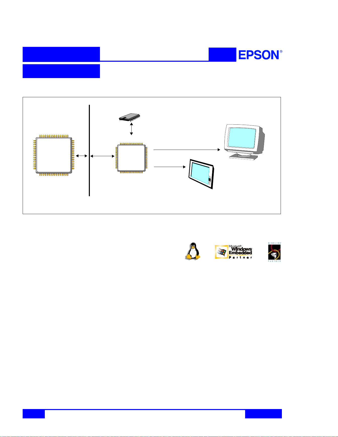
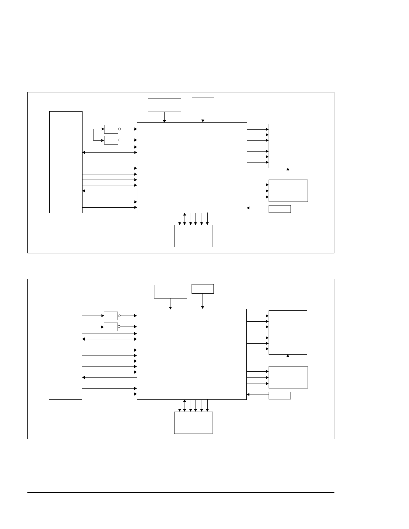
SYSTEM BLOCK DIAGRAM
S1D13505
Flat Panel
Digital Out
CPU
CRT
EDO-DRAM
FPM-DRAM
Analog Out
Data and
Control Signals
CONTACT YOUR SALES REPRESENTATIVE FOR THESE COMPREHENSIVE DESIGN TOOLS
• S1D13505 Technical
Manual
• Linux Console Driver
• S5U13505 Evaluation Boards • Windows
CE Display Driver
• CPU Independent Software
Utilities
•VXWorks
TornadoTM Display
Driver
Copyright © 2001 Epson Research and Development, Inc. All Rights Reserved.
Information in this document is subject t o change without not ice . You may dow n load and use this docum ent, bu t only for you r own use in eva luati ng Sei ko Epson/
EPSON products. You may not modify the document. Epson Research and Devel opment, Inc. disclaims any repr esentati on that the contents of this document are
accurate or current. The Programs/Technologies described in this document may contain material protected under U.S. and/or International Patent laws.
EPSON is a registered trademark of Seiko Epson Corporation. Microsoft, Windows, and the Windows Embedded Partner Logo are registered trademarks of Microsoft Corporation. All other trademarks are the property of their respective owners.
Japan
Seiko Epson Corporation
Electronic Devices Marketing Division
421-8, Hino, Hino-shi
Tokyo 191-8501, Japan
Tel: 042-587-5812
Fax: 042-587-5564
http://www.epson.co.jp/
Hong Kong
Epson Hong Kong Ltd.
20/F., Harbour Centre
25 Harbour Road
Wanchai, Hong Kong
Tel: 2585-4600
Fax: 2827-4346
http://www.epson.com.hk/
Taiwan
Epson Taiwan Technology & Trading Ltd.
10F, No. 287
Nanking East Road
Sec. 3, Taipei, Taiwan
Tel: 02-2717-7360
Fax: 02-2712-9164
http://www.epson.com.tw/
Singapore
Epson Singapore Pte., Ltd.
No. 1
Temasek Avenue #36-00
Millenia Tower
Singapore, 039192
Tel: 337-7911
Fax: 334-2716
http://www.epson.com.sg/
Europe
Epson Europe Electronics GmbH
Riesstrasse 15
80992 Munich, Germany
Tel: 089-14005-0
Fax: 089-14005-110
http://www.epson-electronics.de/
North Amer ica
Epson Electronics America, Inc.
150 River Oaks Parkway
San Jose, CA 95134, USA
Tel: (408) 922-0200
Fax: (408) 922-0238
http://www.eea.epson.com/
Page 6

S1D13505 Embedded RAMDAC LCD/CRT Controller
Hardware Functional Specification
Document Number: X23A-A-001-14
Copyright © 1998, 2001 Epson Research and Development, Inc. All Rights Reserved.
Information in this document is subject to change without notice. You may download and use this document, but only for your own use in
evaluating Seiko Epson/EPSON products. You may not modify the document. Epson Research and Development, Inc. disclaims any
representation that the contents of this document are accurate or current. The Programs/Technologies described in this document may contain
material protected under U.S. and/or International Patent laws.
EPSON is a registered trademark of Seiko Epson Corporation. All other trademarks are the property of their respective owners.
Page 7

Page 2
Epson Research and Development
Vancouver Design Center
S1D13505 Hardware Functional Specification
X23A-A-001-14 Issue Date: 01/02/02
THIS PAGE LEFT BLANK
Page 8

Epson Research and Development
Page 3
Vancouver Design Center
Hardware Functional Specification S1D13505
Issue Date: 01/02/02 X23A-A-001-14
Table of Contents
1 Introduction . . . . . . . . . . . . . . . . . . . . . . . . . . . . . . . . . . . . . . . . . . . . 11
1.1 Scope . . . . . . . . . . . . . . . . . . . . . . . . . . . . . . . . . . . . . 11
1.2 Overview Description . . . . . . . . . . . . . . . . . . . . . . . . . . . . . . . 11
2 Features . . . . . . . . . . . . . . . . . . . . . . . . . . . . . . . . . . . . . . . . . . . . . . 12
2.1 Memory Interface . . . . . . . . . . . . . . . . . . . . . . . . . . . . . . . . . 12
2.2 CPU Interface . . . . . . . . . . . . . . . . . . . . . . . . . . . . . . . . . . 12
2.3 Display Support . . . . . . . . . . . . . . . . . . . . . . . . . . . . . . . . . 13
2.4 Display Modes . . . . . . . . . . . . . . . . . . . . . . . . . . . . . . . . . . 13
2.5 Display Features . . . . . . . . . . . . . . . . . . . . . . . . . . . . . . . . . 13
2.6 Clock Source . . . . . . . . . . . . . . . . . . . . . . . . . . . . . . . . . . 13
2.7 Miscellaneous . . . . . . . . . . . . . . . . . . . . . . . . . . . . . . . . . . 14
3 Typical System Implementation Diagrams . . . . . . . . . . . . . . . . . . . . . . . . . . . 15
4 Internal Description . . . . . . . . . . . . . . . . . . . . . . . . . . . . . . . . . . . . . . . 20
4.1 Block Diagram Showing Datapaths . . . . . . . . . . . . . . . . . . . . . . . . . . 20
4.2 Block Descriptions . . . . . . . . . . . . . . . . . . . . . . . . . . . . . . . . 20
4.2.1 Register . . . . . . . . . . . . . . . . . . . . . . . . . . . . . . . . . . . . . . . . . . . . . 20
4.2.2 Host Interface . . . . . . . . . . . . . . . . . . . . . . . . . . . . . . . . . . . . . . . . . . 20
4.2.3 CPU R/W . . . . . . . . . . . . . . . . . . . . . . . . . . . . . . . . . . . . . . . . . . . . 20
4.2.4 Memory Controller . . . . . . . . . . . . . . . . . . . . . . . . . . . . . . . . . . . . . . . 21
4.2.5 Display FIFO . . . . . . . . . . . . . . . . . . . . . . . . . . . . . . . . . . . . . . . . . . 21
4.2.6 Cursor FIFO . . . . . . . . . . . . . . . . . . . . . . . . . . . . . . . . . . . . . . . . . . . 21
4.2.7 Look-Up Tables . . . . . . . . . . . . . . . . . . . . . . . . . . . . . . . . . . . . . . . . . 21
4.2.8 CRTC . . . . . . . . . . . . . . . . . . . . . . . . . . . . . . . . . . . . . . . . . . . . . . 21
4.2.9 LCD Interface . . . . . . . . . . . . . . . . . . . . . . . . . . . . . . . . . . . . . . . . . . 21
4.2.10 DAC . . . . . . . . . . . . . . . . . . . . . . . . . . . . . . . . . . . . . . . . . . . . . . . 21
4.2.11 Power Save . . . . . . . . . . . . . . . . . . . . . . . . . . . . . . . . . . . . . . . . . . . 21
4.2.12 Clocks . . . . . . . . . . . . . . . . . . . . . . . . . . . . . . . . . . . . . . . . . . . . . . 21
5 Pins . . . . . . . . . . . . . . . . . . . . . . . . . . . . . . . . . . . . . . . . . . . . . . . . 22
5.1 Pinout Diagram . . . . . . . . . . . . . . . . . . . . . . . . . . . . . . . . . . 22
5.2 Pin Description . . . . . . . . . . . . . . . . . . . . . . . . . . . . . . . . . . 23
5.2.1 Host Interface . . . . . . . . . . . . . . . . . . . . . . . . . . . . . . . . . . . . . . . . . . 23
5.2.2 Memory Interface . . . . . . . . . . . . . . . . . . . . . . . . . . . . . . . . . . . . . . . . 29
5.2.3 LCD Interface . . . . . . . . . . . . . . . . . . . . . . . . . . . . . . . . . . . . . . . . . . 31
5.2.4 CRT Interface . . . . . . . . . . . . . . . . . . . . . . . . . . . . . . . . . . . . . . . . . . 31
5.2.5 Miscellaneous . . . . . . . . . . . . . . . . . . . . . . . . . . . . . . . . . . . . . . . . . . 32
5.3 Summary of Configuration Options . . . . . . . . . . . . . . . . . . . . . . . . . . 33
5.4 Multiple Function Pin Mapping . . . . . . . . . . . . . . . . . . . . . . . . . . . 34
5.5 CRT Interface . . . . . . . . . . . . . . . . . . . . . . . . . . . . . . . . . . 37
6 D.C. Characteristics . . . . . . . . . . . . . . . . . . . . . . . . . . . . . . . . . . . . . . . 38
Page 9

Page 4
Epson Research and Development
Vancouver Design Center
S1D13505 Hardware Functional Specification
X23A-A-001-14 Issue Date: 01/02/02
7 A.C. Characteristics . . . . . . . . . . . . . . . . . . . . . . . . . . . . . . . . . . . . . . . 42
7.1 CPU Interface Timing . . . . . . . . . . . . . . . . . . . . . . . . . . . . . . . 42
7.1.1 SH-4 Interface Timing . . . . . . . . . . . . . . . . . . . . . . . . . . . . . . . . . . . . . .42
7.1.2 SH-3 Interface Timing . . . . . . . . . . . . . . . . . . . . . . . . . . . . . . . . . . . . . .44
7.1.3 MC68K Bus 1 Interface Timing (e.g. MC68000) . . . . . . . . . . . . . . . . . . . . . . . .46
7.1.4 MC68K Bus 2 Interface Timing (e.g. MC68030) . . . . . . . . . . . . . . . . . . . . . . . .48
7.1.5 PC Card Interface Timing . . . . . . . . . . . . . . . . . . . . . . . . . . . . . . . . . . . .50
7.1.6 Generic Interface Timing . . . . . . . . . . . . . . . . . . . . . . . . . . . . . . . . . . . . .52
7.1.7 MIPS/ISA Interface Timing . . . . . . . . . . . . . . . . . . . . . . . . . . . . . . . . . . .54
7.1.8 Philips Interface Timing (e.g. PR31500/PR31700) . . . . . . . . . . . . . . . . . . . . . . .56
7.1.9 Toshiba Interface Timing (e.g. TX3912) . . . . . . . . . . . . . . . . . . . . . . . . . . . . .58
7.1.10 Power PC Interface Timing (e.g. MPC8xx, MC68040, Coldfire) . . . . . . . . . . . . . . . .60
7.2 Clock Input Requirements . . . . . . . . . . . . . . . . . . . . . . . . . . . . . 62
7.3 Memory Interface Timing . . . . . . . . . . . . . . . . . . . . . . . . . . . . . 63
7.3.1 EDO-DRAM Read/Write/Read-Write Timing . . . . . . . . . . . . . . . . . . . . . . . . . .63
7.3.2 EDO-DRAM CAS Before RAS Refresh Timing . . . . . . . . . . . . . . . . . . . . . . . .66
7.3.3 EDO-DRAM Self-Refresh Timing . . . . . . . . . . . . . . . . . . . . . . . . . . . . . . . .68
7.3.4 FPM-DRAM Read/Write/Read-Write Timing . . . . . . . . . . . . . . . . . . . . . . . . . .69
7.3.5 FPM-DRAM CAS Before RAS Refresh Timing . . . . . . . . . . . . . . . . . . . . . . . .72
7.3.6 FPM-DRAM Self-Refresh Timing . . . . . . . . . . . . . . . . . . . . . . . . . . . . . . . .73
7.4 Power Sequencing . . . . . . . . . . . . . . . . . . . . . . . . . . . . . . . . 74
7.4.1 LCD Power Sequencing . . . . . . . . . . . . . . . . . . . . . . . . . . . . . . . . . . . . .74
7.4.2 Power Save Status . . . . . . . . . . . . . . . . . . . . . . . . . . . . . . . . . . . . . . . .75
7.5 Display Interface . . . . . . . . . . . . . . . . . . . . . . . . . . . . . . . . . 76
7.5.1 4-Bit Single Monochrome Passive LCD Panel Timing . . . . . . . . . . . . . . . . . . . . .76
7.5.2 8-Bit Single Monochrome Passive LCD Panel Timing . . . . . . . . . . . . . . . . . . . . .78
7.5.3 4-Bit Single Color Passive LCD Panel Timing . . . . . . . . . . . . . . . . . . . . . . . . .80
7.5.4 8-Bit Single Color Passive LCD Panel Timing (Format 1) . . . . . . . . . . . . . . . . . . .82
7.5.5 8-Bit Single Color Passive LCD Panel Timing (Format 2) . . . . . . . . . . . . . . . . . . .84
7.5.6 16-Bit Single Color Passive LCD Panel Timing . . . . . . . . . . . . . . . . . . . . . . . . .86
7.5.7 8-Bit Dual Monochrome Passive LCD Panel Timing . . . . . . . . . . . . . . . . . . . . . .88
7.5.8 8-Bit Dual Color Passive LCD Panel Timing . . . . . . . . . . . . . . . . . . . . . . . . . .90
7.5.9 16-Bit Dual Color Passive LCD Panel Timing . . . . . . . . . . . . . . . . . . . . . . . . . .92
7.5.10 16-Bit TFT/D-TFD Panel Timing . . . . . . . . . . . . . . . . . . . . . . . . . . . . . . . .94
7.5.11 CRT Timing . . . . . . . . . . . . . . . . . . . . . . . . . . . . . . . . . . . . . . . . . . .97
8 Registers . . . . . . . . . . . . . . . . . . . . . . . . . . . . . . . . . . . . . . . . . . . . . 99
8.1 Register Mapping . . . . . . . . . . . . . . . . . . . . . . . . . . . . . . . . 99
8.2 Register Descriptions . . . . . . . . . . . . . . . . . . . . . . . . . . . . . . . 99
8.2.1 Revision Code Register . . . . . . . . . . . . . . . . . . . . . . . . . . . . . . . . . . . . .99
8.2.2 Memory Configuration Registers . . . . . . . . . . . . . . . . . . . . . . . . . . . . . . . 100
8.2.3 Panel/Monitor Configuration Registers . . . . . . . . . . . . . . . . . . . . . . . . . . . . 101
8.2.4 Display Configuration Registers . . . . . . . . . . . . . . . . . . . . . . . . . . . . . . . . 106
Page 10

Epson Research and Development
Page 5
Vancouver Design Center
Hardware Functional Specification S1D13505
Issue Date: 01/02/02 X23A-A-001-14
8.2.5 Clock Configuration Register . . . . . . . . . . . . . . . . . . . . . . . . . . . . . . . . . 110
8.2.6 Power Save Configuration Registers . . . . . . . . . . . . . . . . . . . . . . . . . . . . . 110
8.2.7 Miscellaneous Registers . . . . . . . . . . . . . . . . . . . . . . . . . . . . . . . . . . . . 111
8.2.8 Look-Up Table Registers . . . . . . . . . . . . . . . . . . . . . . . . . . . . . . . . . . . 117
8.2.9 Ink/Cursor Registers . . . . . . . . . . . . . . . . . . . . . . . . . . . . . . . . . . . . . . 118
9 Display Buffer . . . . . . . . . . . . . . . . . . . . . . . . . . . . . . . . . . . . . . . . . . .122
9.1 Image Buffer . . . . . . . . . . . . . . . . . . . . . . . . . . . . . . . . . . .123
9.2 Ink/Cursor Buffers . . . . . . . . . . . . . . . . . . . . . . . . . . . . . . . .123
9.3 Half Frame Buffer . . . . . . . . . . . . . . . . . . . . . . . . . . . . . . . .123
10 Display Configuration . . . . . . . . . . . . . . . . . . . . . . . . . . . . . . . . . . . . . .124
10.1 Display Mode Data Format . . . . . . . . . . . . . . . . . . . . . . . . . . . . .124
10.2 Image Manipulation . . . . . . . . . . . . . . . . . . . . . . . . . . . . . . . .126
11 Look-Up Table Architecture . . . . . . . . . . . . . . . . . . . . . . . . . . . . . . . . . . .127
11.1 Monochrome Modes . . . . . . . . . . . . . . . . . . . . . . . . . . . . . . . .127
11.2 Color Modes . . . . . . . . . . . . . . . . . . . . . . . . . . . . . . . . . . .129
12 Ink/Cursor Architecture . . . . . . . . . . . . . . . . . . . . . . . . . . . . . . . . . . . . .133
12.1 Ink/Cursor Buffers . . . . . . . . . . . . . . . . . . . . . . . . . . . . . . . .133
12.2 Ink/Cursor Data Format . . . . . . . . . . . . . . . . . . . . . . . . . . . . . .133
12.3 Ink/Cursor Image Manipulation . . . . . . . . . . . . . . . . . . . . . . . . . . .134
12.3.1 Ink Image . . . . . . . . . . . . . . . . . . . . . . . . . . . . . . . . . . . . . . . . . . . 134
12.3.2 Cursor Image . . . . . . . . . . . . . . . . . . . . . . . . . . . . . . . . . . . . . . . . . 134
13 SwivelView™ . . . . . . . . . . . . . . . . . . . . . . . . . . . . . . . . . . . . . . . . . . .135
13.1 Concept . . . . . . . . . . . . . . . . . . . . . . . . . . . . . . . . . . . . .135
13.2 Image Manipulation in SwivelView . . . . . . . . . . . . . . . . . . . . . . . . . .136
13.3 Physical Memory Requirement . . . . . . . . . . . . . . . . . . . . . . . . . . .137
13.4 Limitations . . . . . . . . . . . . . . . . . . . . . . . . . . . . . . . . . . .138
14 Clocking . . . . . . . . . . . . . . . . . . . . . . . . . . . . . . . . . . . . . . . . . . . . . .139
14.1 Maximum MCLK: PCLK Ratios . . . . . . . . . . . . . . . . . . . . . . . . . . .139
14.2 Frame Rate Calculation . . . . . . . . . . . . . . . . . . . . . . . . . . . . . .141
14.3 Bandwidth Calculation . . . . . . . . . . . . . . . . . . . . . . . . . . . . . . .143
15 Power Save Modes . . . . . . . . . . . . . . . . . . . . . . . . . . . . . . . . . . . . . . . .147
16 Mechanical Data . . . . . . . . . . . . . . . . . . . . . . . . . . . . . . . . . . . . . . . . .148
Page 11

Page 6
Epson Research and Development
Vancouver Design Center
S1D13505 Hardware Functional Specification
X23A-A-001-14 Issue Date: 01/02/02
THIS PAGE LEFT BLANK
Page 12

Epson Research and Development
Page 7
Vancouver Design Center
Hardware Functional Specification S1D13505
Issue Date: 01/02/02 X23A-A-001-14
List of Tables
Table 5-1: Host Interface Pin Descriptions. . . . . . . . . . . . . . . . . . . . . . . . . . . . . . . . . . . . 23
Table 5-2: Memory Interface Pin Descriptions. . . . . . . . . . . . . . . . . . . . . . . . . . . . . . . . . . 29
Table 5-2: LCD Interface Pin Descriptions. . . . . . . . . . . . . . . . . . . . . . . . . . . . . . . . . . . . 31
Table 5-3: CRT Interface Pin Descriptions. . . . . . . . . . . . . . . . . . . . . . . . . . . . . . . . . . . . 31
Table 5-4: Miscellaneous Interface Pin Descriptions. . . . . . . . . . . . . . . . . . . . . . . . . . . . . . . 32
Table 5-5: Summary of Power On/Reset Options . . . . . . . . . . . . . . . . . . . . . . . . . . . . . . . . 33
Table 5-6: CPU Interface Pin Mapping. . . . . . . . . . . . . . . . . . . . . . . . . . . . . . . . . . . . . . 34
Table 5-7: Memory Interface Pin Mapping. . . . . . . . . . . . . . . . . . . . . . . . . . . . . . . . . . . . 35
Table 5-8: LCD Interface Pin Mapping . . . . . . . . . . . . . . . . . . . . . . . . . . . . . . . . . . . . . 36
Table 6-1: Absolute Maximum Ratings . . . . . . . . . . . . . . . . . . . . . . . . . . . . . . . . . . . . . 38
Table 6-2: Recommended Operating Conditions. . . . . . . . . . . . . . . . . . . . . . . . . . . . . . . . . 38
Table 6-3: Electrical Characteristics for VDD = 5.0V typical . . . . . . . . . . . . . . . . . . . . . . . . . . 39
Table 6-4: Electrical Characteristics for VDD = 3.3V typical . . . . . . . . . . . . . . . . . . . . . . . . . . 40
Table 6-5: Electrical Characteristics for VDD = 3.0V typical . . . . . . . . . . . . . . . . . . . . . . . . . . 41
Table 7-1: SH-4 Timing . . . . . . . . . . . . . . . . . . . . . . . . . . . . . . . . . . . . . . . . . . . . . 43
Table 7-2: SH-3 Timing . . . . . . . . . . . . . . . . . . . . . . . . . . . . . . . . . . . . . . . . . . . . . 45
Table 7-3: MC68000 Timing . . . . . . . . . . . . . . . . . . . . . . . . . . . . . . . . . . . . . . . . . . . 47
Table 7-4: MC68030 Timing . . . . . . . . . . . . . . . . . . . . . . . . . . . . . . . . . . . . . . . . . . . 49
Table 7-5: PC Card Timing. . . . . . . . . . . . . . . . . . . . . . . . . . . . . . . . . . . . . . . . . . . . 51
Table 7-6: Generic Timing . . . . . . . . . . . . . . . . . . . . . . . . . . . . . . . . . . . . . . . . . . . . 53
Table 7-7: MIPS/ISA Timing. . . . . . . . . . . . . . . . . . . . . . . . . . . . . . . . . . . . . . . . . . . 55
Table 7-8: Philips Timing. . . . . . . . . . . . . . . . . . . . . . . . . . . . . . . . . . . . . . . . . . . . . 57
Table 7-9: Clock Input Requirements for BUSCLK using Philips local bus. . . . . . . . . . . . . . . . . . . 57
Table 7-10: Toshiba Timing . . . . . . . . . . . . . . . . . . . . . . . . . . . . . . . . . . . . . . . . . . . . 59
Table 7-11: Clock Input Requirements for BUSCLK using Toshiba local bus . . . . . . . . . . . . . . . . . . 59
Table 7-12: Power PC Timing . . . . . . . . . . . . . . . . . . . . . . . . . . . . . . . . . . . . . . . . . . . 61
Table 7-13: Clock Input Requirements for CLKI divided down internally (MCLK = CLKI/2) . . . . . . . . . 62
Table 7-14: Clock Input Requirements for CLKI . . . . . . . . . . . . . . . . . . . . . . . . . . . . . . . . . 62
Table 7-15: EDO-DRAM Read/Write/Read-Write Timing . . . . . . . . . . . . . . . . . . . . . . . . . . . . 64
Table 7-16: EDO-DRAM CAS Before RAS Refresh Timing. . . . . . . . . . . . . . . . . . . . . . . . . . . 66
Table 7-17: EDO-DRAM Self-Refresh Timing . . . . . . . . . . . . . . . . . . . . . . . . . . . . . . . . . . 68
Table 7-18: FPM-DRAM Read/Write/Read-Write Timing . . . . . . . . . . . . . . . . . . . . . . . . . . . . 70
Table 7-19: FPM-DRAM CAS Before RAS Refresh Timing . . . . . . . . . . . . . . . . . . . . . . . . . . . 72
Table 7-20: FPM-DRAM CBR Self-Refresh Timing . . . . . . . . . . . . . . . . . . . . . . . . . . . . . . . 73
Table 7-21: LCD Panel Power Off/ Power On. . . . . . . . . . . . . . . . . . . . . . . . . . . . . . . . . . . 74
Table 7-22: Power Save Status and Local Bus Memory Access Relative to Power Save Mode . . . . . . . . . 75
Table 7-23: 4-Bit Single Monochrome Passive LCD Panel A.C. Timing. . . . . . . . . . . . . . . . . . . . . 77
Table 7-24: 8-Bit Single Monochrome Passive LCD Panel A.C. Timing. . . . . . . . . . . . . . . . . . . . . 79
Table 7-25: 4-Bit Single Color Passive LCD Panel A.C. Timing . . . . . . . . . . . . . . . . . . . . . . . . . 81
Table 7-26: 8-Bit Single Color Passive LCD Panel A.C. Timing (Format 1) . . . . . . . . . . . . . . . . . . . 83
Page 13

Page 8
Epson Research and Development
Vancouver Design Center
S1D13505 Hardware Functional Specification
X23A-A-001-14 Issue Date: 01/02/02
Table 7-27: 8-Bit Single Color Passive LCD Panel A.C. Timing (Format 2) . . . . . . . . . . . . . . . . . . .85
Table 7-28: 16-Bit Single Color Passive LCD Panel A.C. Timing. . . . . . . . . . . . . . . . . . . . . . . . .87
Table 7-29: 8-Bit Dual Monochrome Passive LCD Panel A.C. Timing . . . . . . . . . . . . . . . . . . . . . .89
Table 7-30: 8-Bit Dual Color Passive LCD Panel A.C. Timing . . . . . . . . . . . . . . . . . . . . . . . . . .91
Table 7-31: 16-Bit Dual Color Passive LCD Panel A.C. Timing . . . . . . . . . . . . . . . . . . . . . . . . .93
Table 7-32: TFT/D-TFD A.C. Timing . . . . . . . . . . . . . . . . . . . . . . . . . . . . . . . . . . . . . . .96
Table 8-1: S1D13505 Addressing. . . . . . . . . . . . . . . . . . . . . . . . . . . . . . . . . . . . . . . . .99
Table 8-2: DRAM Refresh Rate Selection . . . . . . . . . . . . . . . . . . . . . . . . . . . . . . . . . . . 100
Table 8-3: Panel Data Width Selection . . . . . . . . . . . . . . . . . . . . . . . . . . . . . . . . . . . . . 101
Table 8-4: FPLINE Polarity Selection . . . . . . . . . . . . . . . . . . . . . . . . . . . . . . . . . . . . . 103
Table 8-5: FPFRAME Polarity Selection . . . . . . . . . . . . . . . . . . . . . . . . . . . . . . . . . . . . 105
Table 8-6: Simultaneous Display Option Selection . . . . . . . . . . . . . . . . . . . . . . . . . . . . . . . 106
Table 8-7: Bit-per-pixel Selection. . . . . . . . . . . . . . . . . . . . . . . . . . . . . . . . . . . . . . . . 107
Table 8-8: Pixel Panning Selection . . . . . . . . . . . . . . . . . . . . . . . . . . . . . . . . . . . . . . . 109
Table 8-9: PCLK Divide Selection . . . . . . . . . . . . . . . . . . . . . . . . . . . . . . . . . . . . . . . 110
Table 8-10: Suspend Refresh Selection. . . . . . . . . . . . . . . . . . . . . . . . . . . . . . . . . . . . . . 111
Table 8-11: MA/GPIO Pin Functionality. . . . . . . . . . . . . . . . . . . . . . . . . . . . . . . . . . . . . 112
Table 8-12: Minimum Memory Timing Selection . . . . . . . . . . . . . . . . . . . . . . . . . . . . . . . . 114
Table 8-13: RAS#-to-CAS# Delay Timing Select . . . . . . . . . . . . . . . . . . . . . . . . . . . . . . . . 115
Table 8-14: RAS Precharge Timing Select . . . . . . . . . . . . . . . . . . . . . . . . . . . . . . . . . . . . 116
Table 8-15: Optimal NRC, NRP, and NRCD values at maximum MCLK frequency . . . . . . . . . . . . . . 116
Table 8-16: Minimum Memory Timing Selection . . . . . . . . . . . . . . . . . . . . . . . . . . . . . . . . 117
Table 8-17: Ink/Cursor Selection . . . . . . . . . . . . . . . . . . . . . . . . . . . . . . . . . . . . . . . . . 118
Table 8-18: Ink/Cursor Start Address Encoding . . . . . . . . . . . . . . . . . . . . . . . . . . . . . . . . . 120
Table 8-19: Recommended Alternate FRM Scheme . . . . . . . . . . . . . . . . . . . . . . . . . . . . . . . 121
Table 9-1: S1D13505 Addressing. . . . . . . . . . . . . . . . . . . . . . . . . . . . . . . . . . . . . . . . 122
Table 12-1: Ink/Cursor Start Address Encoding . . . . . . . . . . . . . . . . . . . . . . . . . . . . . . . . . 133
Table 12-2: Ink/Cursor Color Select . . . . . . . . . . . . . . . . . . . . . . . . . . . . . . . . . . . . . . . 134
Table 13-2 Minimum DRAM Size Required for SwivelView. . . . . . . . . . . . . . . . . . . . . . . . . . 138
Table 14-1: Maximum PCLK Frequency with EDO-DRAM . . . . . . . . . . . . . . . . . . . . . . . . . . 139
Table 14-2: Maximum PCLK Frequency with FPM-DRAM . . . . . . . . . . . . . . . . . . . . . . . . . . 140
Table 14-3: Example Frame Rates with Ink Disabled . . . . . . . . . . . . . . . . . . . . . . . . . . . . . . 141
Table 14-4: Number of MCLKs required for various memory access . . . . . . . . . . . . . . . . . . . . . . 143
Table 14-5: Total # MCLKs taken for Display refresh. . . . . . . . . . . . . . . . . . . . . . . . . . . . . . 144
Table 14-6: Theoretical Maximum Bandwidth M byte/sec, Cursor/Ink disabled . . . . . . . . . . . . . . . . 145
Table 15-1: Power Save Mode Function Summary . . . . . . . . . . . . . . . . . . . . . . . . . . . . . . . 147
Table 15-2: Pin States in Power-save Modes. . . . . . . . . . . . . . . . . . . . . . . . . . . . . . . . . . . 147
Page 14

Epson Research and Development
Page 9
Vancouver Design Center
Hardware Functional Specification S1D13505
Issue Date: 01/02/02 X23A-A-001-14
List of Figures
Figure 3-1: Typical System Diagram (SH-4 Bus) . . . . . . . . . . . . . . . . . . . . . . . . . . . . . . . 15
Figure 3-2: Typical System Diagram (SH-3 Bus) . . . . . . . . . . . . . . . . . . . . . . . . . . . . . . . 15
Figure 3-3: Typical System Diagram (MC68K Bus 1, 16-Bit 68000) . . . . . . . . . . . . . . . . . . . . . 16
Figure 3-4: Typical System Diagram (MC68K Bus 2, 32-Bit 68030) . . . . . . . . . . . . . . . . . . . . . 16
Figure 3-5: Typical System Diagram (Generic Bus) . . . . . . . . . . . . . . . . . . . . . . . . . . . . . . 17
Figure 3-6: Typical System Diagram (NEC VR41xx (MIPS) Bus) . . . . . . . . . . . . . . . . . . . . . . 17
Figure 3-7: Typical System Diagram (Philips PR31500/PR31700 Bus). . . . . . . . . . . . . . . . . . . . 18
Figure 3-8: Typical System Diagram (Toshiba TX3912 Bus) . . . . . . . . . . . . . . . . . . . . . . . . . 18
Figure 3-9: Typical System Diagram (Power PC Bus). . . . . . . . . . . . . . . . . . . . . . . . . . . . . 19
Figure 3-10: Typical System Diagram (PC Card (PCMCIA) Bus) . . . . . . . . . . . . . . . . . . . . . . . 19
Figure 5-1: Pinout Diagram. . . . . . . . . . . . . . . . . . . . . . . . . . . . . . . . . . . . . . . . . . . 22
Figure 5-3: External Circuitry for CRT Interface . . . . . . . . . . . . . . . . . . . . . . . . . . . . . . . 37
Figure 7-1: SH-4 Timing . . . . . . . . . . . . . . . . . . . . . . . . . . . . . . . . . . . . . . . . . . . . 42
Figure 7-2: SH-3 Timing . . . . . . . . . . . . . . . . . . . . . . . . . . . . . . . . . . . . . . . . . . . . 44
Figure 7-3: MC68000 Timing . . . . . . . . . . . . . . . . . . . . . . . . . . . . . . . . . . . . . . . . . 46
Figure 7-4: MC68030 Timing . . . . . . . . . . . . . . . . . . . . . . . . . . . . . . . . . . . . . . . . . 48
Figure 7-5: PC Card Timing . . . . . . . . . . . . . . . . . . . . . . . . . . . . . . . . . . . . . . . . . . 50
Figure 7-6: Generic Timing. . . . . . . . . . . . . . . . . . . . . . . . . . . . . . . . . . . . . . . . . . . 52
Figure 7-7: MIPS/ISA Timing . . . . . . . . . . . . . . . . . . . . . . . . . . . . . . . . . . . . . . . . . 54
Figure 7-8: Philips Timing . . . . . . . . . . . . . . . . . . . . . . . . . . . . . . . . . . . . . . . . . . . 56
Figure 7-9: Clock Input Requirement . . . . . . . . . . . . . . . . . . . . . . . . . . . . . . . . . . . . . 57
Figure 7-10: Toshiba Timing . . . . . . . . . . . . . . . . . . . . . . . . . . . . . . . . . . . . . . . . . . 58
Figure 7-11: Clock Input Requirement . . . . . . . . . . . . . . . . . . . . . . . . . . . . . . . . . . . . . 59
Figure 7-12: Power PC Timing . . . . . . . . . . . . . . . . . . . . . . . . . . . . . . . . . . . . . . . . . 60
Figure 7-13: Clock Input Requirement . . . . . . . . . . . . . . . . . . . . . . . . . . . . . . . . . . . . . 62
Figure 7-14: EDO-DRAM Read/Write Timing . . . . . . . . . . . . . . . . . . . . . . . . . . . . . . . . . 63
Figure 7-15: EDO-DRAM Read-Write Timing . . . . . . . . . . . . . . . . . . . . . . . . . . . . . . . . . 64
Figure 7-16: EDO-DRAM CAS Before RAS Refresh Timing . . . . . . . . . . . . . . . . . . . . . . . . . 66
Figure 7-17: EDO-DRAM Self-Refresh Timing . . . . . . . . . . . . . . . . . . . . . . . . . . . . . . . . 68
Figure 7-18: FPM-DRAM Read/Write Timing . . . . . . . . . . . . . . . . . . . . . . . . . . . . . . . . . 69
Figure 7-19: FPM-DRAM Read-Write Timing . . . . . . . . . . . . . . . . . . . . . . . . . . . . . . . . . 70
Figure 7-20: FPM-DRAM CAS Before RAS Refresh Timing . . . . . . . . . . . . . . . . . . . . . . . . . 72
Figure 7-21: FPM-DRAM Self-Refresh Timing. . . . . . . . . . . . . . . . . . . . . . . . . . . . . . . . . 73
Figure 7-22: LCD Panel Power Off / Power On Timing. Drawn with LCDPWR set to active high polarity. . 74
Figure 7-23: Power Save Status and Local Bus Memory Access Relative to Power Save Mode. . . . . . . . 75
Figure 7-24: 4-Bit Single Monochrome Passive LCD Panel Timing . . . . . . . . . . . . . . . . . . . . . . 76
Figure 7-25: 4-Bit Single Monochrome Passive LCD Panel A.C. Timing . . . . . . . . . . . . . . . . . . . 77
Figure 7-26: 8-Bit Single Monochrome Passive LCD Panel Timing . . . . . . . . . . . . . . . . . . . . . . 78
Figure 7-27: 8-Bit Single Monochrome Passive LCD Panel A.C. Timing . . . . . . . . . . . . . . . . . . . 79
Figure 7-28: 4-Bit Single Color Passive LCD Panel Timing . . . . . . . . . . . . . . . . . . . . . . . . . . 80
Figure 7-29: 4-Bit Single Color Passive LCD Panel A.C. Timing . . . . . . . . . . . . . . . . . . . . . . . 81
Page 15

Page 10
Epson Research and Development
Vancouver Design Center
S1D13505 Hardware Functional Specification
X23A-A-001-14 Issue Date: 01/02/02
Figure 7-30: 8-Bit Single Color Passive LCD Panel Timing (Format 1). . . . . . . . . . . . . . . . . . . . . 82
Figure 7-31: 8-Bit Single Color Passive LCD Panel A.C. Timing (Format 1). . . . . . . . . . . . . . . . . . 83
Figure 7-32: 8-Bit Single Color Passive LCD Panel Timing (Format 2). . . . . . . . . . . . . . . . . . . . . 84
Figure 7-33: 8-Bit Single Color Passive LCD Panel A.C. Timing (Format 2). . . . . . . . . . . . . . . . . . 85
Figure 7-34: 16-Bit Single Color Passive LCD Panel Timing . . . . . . . . . . . . . . . . . . . . . . . . . .86
Figure 7-35: 16-Bit Single Color Passive LCD Panel A.C. Timing . . . . . . . . . . . . . . . . . . . . . . .87
Figure 7-36: 8-Bit Dual Monochrome Passive LCD Panel Timing . . . . . . . . . . . . . . . . . . . . . . .88
Figure 7-37: 8-Bit Dual Monochrome Passive LCD Panel A.C. Timing . . . . . . . . . . . . . . . . . . . . 89
Figure 7-38: 8-Bit Dual Color Passive LCD Panel Timing . . . . . . . . . . . . . . . . . . . . . . . . . . . 90
Figure 7-39: 8-Bit Dual Color Passive LCD Panel A.C. Timing . . . . . . . . . . . . . . . . . . . . . . . . . 91
Figure 7-40: 16-Bit Dual Color Passive LCD Panel Timing . . . . . . . . . . . . . . . . . . . . . . . . . . . 92
Figure 7-41: 16-Bit Dual Color Passive LCD Panel A.C. Timing . . . . . . . . . . . . . . . . . . . . . . . . 93
Figure 7-42: 16-Bit TFT/D-TFD Panel Timing . . . . . . . . . . . . . . . . . . . . . . . . . . . . . . . . . 94
Figure 7-43: TFT/D-TFD A.C. Timing. . . . . . . . . . . . . . . . . . . . . . . . . . . . . . . . . . . . . .95
Figure 7-44: CRT Timing. . . . . . . . . . . . . . . . . . . . . . . . . . . . . . . . . . . . . . . . . . . . .97
Figure 7-45: CRT A.C. Timing. . . . . . . . . . . . . . . . . . . . . . . . . . . . . . . . . . . . . . . . . . 98
Figure 9-1: Display Buffer Addressing . . . . . . . . . . . . . . . . . . . . . . . . . . . . . . . . . . . . 122
Figure 10-1: 1/2/4/8 Bit-per-pixel Format Memory Organization . . . . . . . . . . . . . . . . . . . . . . . 124
Figure 10-2: 15/16 Bit-per-pixel Format Memory Organization. . . . . . . . . . . . . . . . . . . . . . . . 125
Figure 10-3: Image Manipulation. . . . . . . . . . . . . . . . . . . . . . . . . . . . . . . . . . . . . . . . 126
Figure 11-1: 1 Bit-per-pixel Monochrome Mode Data Output Path . . . . . . . . . . . . . . . . . . . . . . 127
Figure 11-2: 2 Bit-per-pixel Monochrome Mode Data Output Path . . . . . . . . . . . . . . . . . . . . . . 127
Figure 11-3: 4 Bit-per-pixel Monochrome Mode Data Output Path . . . . . . . . . . . . . . . . . . . . . . 128
Figure 11-4: 1 Bit-per-pixel Color Mode Data Output Path . . . . . . . . . . . . . . . . . . . . . . . . . . 129
Figure 11-5: 2 Bit-per-pixel Color Mode Data Output Path . . . . . . . . . . . . . . . . . . . . . . . . . . 130
Figure 11-6: 4 Bit-per-pixel Color Mode Data Output Path . . . . . . . . . . . . . . . . . . . . . . . . . . 131
Figure 11-7: 8 Bit-per-pixel Color Mode Data Output Path . . . . . . . . . . . . . . . . . . . . . . . . . . 132
Figure 12-1: Ink/Cursor Data Format. . . . . . . . . . . . . . . . . . . . . . . . . . . . . . . . . . . . . . 133
Figure 12-2: Cursor Positioning . . . . . . . . . . . . . . . . . . . . . . . . . . . . . . . . . . . . . . . . 134
Figure 13-1: Relationship Between The Screen Image and the Image Residing in the Display Buffer . . . . 135
Figure 16-1: Mechanical Drawing QFP15 . . . . . . . . . . . . . . . . . . . . . . . . . . . . . . . . . . . 148
Page 16

Epson Research and Development
Page 11
Vancouver Design Center
Hardware Functional Specification S1D13505
Issue Date: 01/02/02 X23A-A-001-14
1 Introduction
1.1 Scope
This is the Hardware Functional Specification for the S1D13505 Embedded RAMDAC LCD/CRT
Controller. Included in this document are timing diagrams, AC and DC characteristics, register
descriptions, and power management descriptions. This document is intended for two audiences:
Video Subsystem Designers and Soft w are Develop e rs .
This specification will be updated as appropriate. Please check the Epson Electronics America
Website at http://www.eea.epson.com or the Epson Research and Development website at
http://www.erd.epson.com for the latest revision of this document bef ore beginning any development.
We appreciate your comments on our documentation. Please contact us via email at
documentation@erd.epson.com.
1.2 Overview Description
The S1D13505 is a color/monochrome LCD/CRT graphics con troller interfacing to a wide range of
CPUs and display devices. The S1D13505 architecture is designed to meet the low cost, lo w power
requirements of the embedded markets, such as Mobile Communications, Hand-Held PCs, and
Office Automation.
The S1D13505 supports multiple CPUs, all LCD panel types, CRT, and additionally provides a
number of differentiating featur es. Products requi ring a “Portrait” mode display can take advan tage
of the SwivelView™ feature. Simultaneous, Virtual and Split Screen Display are just some of the
display modes supported, while the Hardware Cursor, Ink Layer, and the Memory Enhancement
Registers offer substantial performance benefits. These features, combined with the S1D13505’s
Operating System independence, make it an ideal display solution for a wide variety of applications.
Page 17

Page 12
Epson Research and Development
Vancouver Design Center
S1D13505 Hardware Functional Specification
X23A-A-001-14 Issue Date: 01/02/02
2 Features
2.1 Memory Interface
• 16-bit DRAM interface:
• EDO-DRAM up to 40MHz data rate (80M bytes/sec.).
• FPM-DRAM up to 25MHz data rate (50M bytes/sec.).
• Memory size options:
• 512K bytes using one 256K×16 device.
• 2M bytes using one 1M×16 device.
• Performance Enhancement Register to tailor the memory control output timing for the DRAM
device.
2.2 CPU Interface
• Supports the following interfaces:
• 8/16-bit SH-4 bus interface.
• 8/16-bit SH-3 bus interface.
• 8/16-bit interface to 8/16/32-bit MC68000 microprocessors/microcontrollers.
• 8/16-bit interface to 8/16/32-bit MC68030 microprocessors/microcontrollers.
• Philips PR31500/PR31700 (MIPS).
• Toshiba TX3912 (MIPS)
• 16-bit Power PC (MPC821) microprocessor.
• 16-bit Epson E0C33 microprocessor.
• PC Card (PCMCIA).
• StrongARM (PC Card).
• NEC VR41xx (MIPS).
• ISA bus.
• Supports the following interface with external logic:
• GX486 microprocess or.
• One-stage write buffer for minimum wait-state CPU writes.
• Registers are memory-mapped – the M/R# pin selects between the display buffer and register
address space.
• The complete 2M byte display buffer address space is addressable as a single linear address
space through the 21-bit address bus.
Page 18

Epson Research and Development
Page 13
Vancouver Design Center
Hardware Functional Specification S1D13505
Issue Date: 01/02/02 X23A-A-001-14
2.3 Display Support
• 4/8-bit monochrome passive LCD interface.
• 4/8/16-bit color passive LCD interface.
• Single-panel, single -driv e displ ays .
• Dual-panel, dual-drive displays.
• Direct support for 9/12-bit TFT/D-TFD; 18-bit TFT/D-TFD is supported up to 64K color depth
(16-bit data).
• Embedded RAMDAC (DAC)with direct analog CRT drive.
• Simultaneous display of CRT and passive or TFT/D-TFD panels.
2.4 Display Modes
• 1/2/4/8/15/16 bit-per-pixel (bpp) support on LCD/CRT.
• Up to 16 shades of gray using FRM on monochrome passive LCD panels.
• Up to 4096 colors on passive LCD panels; three 256x4 Look-Up Tables (LUT) are used to map
1/2/4/8 bpp modes into these colors, 15/16 bpp modes are mapped directly using the 4 most
significant bits of the red, green and blue colors.
• Up to 64K colors on TFT/D-TF D LCD panels and CRT; three 2 56x4 Look- Up Tables are us ed to
map 1/2/4/8 bpp modes into 4096 colors, 15/16 bpp modes are mapped directly.
2.5 Display Features
• SwivelView™: direct hardware 90° rotation of display image for “portrait” mode display.
• Split Screen Display: allows two different images to be simultaneously viewed on th e same
display.
• Virtual Display Support: displays images larger than the display size thr ough the use of panning.
• Double Buffering/multi-pages: provides smooth animation and instantaneous screen update.
• Acceleration of screen updates by allocating full display memory bandwidth to CPU (see
REG[23h] bit 7).
• Hardware 64x64 pixel 2-bit cursor or full screen 2-bit ink layer.
• Simultaneous display of CRT and passive panel or TFT/D-TFD panel.
• Normal mode for cases where LCD and CRT screen sizes are identical.
• Line-doubling for simultaneous display of 240-line images on 240-line LCD and 480-line
CRT.
• Even-scan or interlace modes for simultaneous display of 480-line images on 240-line LCD
and 480-line CRT.
2.6 Clock Source
• Single clock input for both the pixel and memory clocks.
• Memory clock can be input clock or (input clock/2), providing flexibility to use CPU bus clock
as input.
• Pixel clock can be the memory clock, (memory cloc k/2), (memor y clock/3 ) or (memory clock/4).
Page 19

Page 14
Epson Research and Development
Vancouver Design Center
S1D13505 Hardware Functional Specification
X23A-A-001-14 Issue Date: 01/02/02
2.7 Miscellaneous
• The memor y data bus, MD[15:0], is used to configure the chip at power-on.
• Three General Purpose Input/Output pins, GPIO[3:1], are available if the upper Memory
Address pins are not required for asymmetric DRAM support.
• Suspend power save mode can be initiated by either hardware or software.
• The SUSPEND# pin is used either as an input to initiate Suspend mode, or as a General Purpose
Output that can be used to control the LCD backlight. Power-on polarity is selected by an MD
configuration pin.
• Operating voltages from 2.7 volts to 5.5 volts are supported
• 128-pin QFP15 surface mount package
Page 20
Epson Research and Development
Page 15
Vancouver Design Center
Hardware Functional Specification S1D13505
Issue Date: 01/02/02 X23A-A-001-14
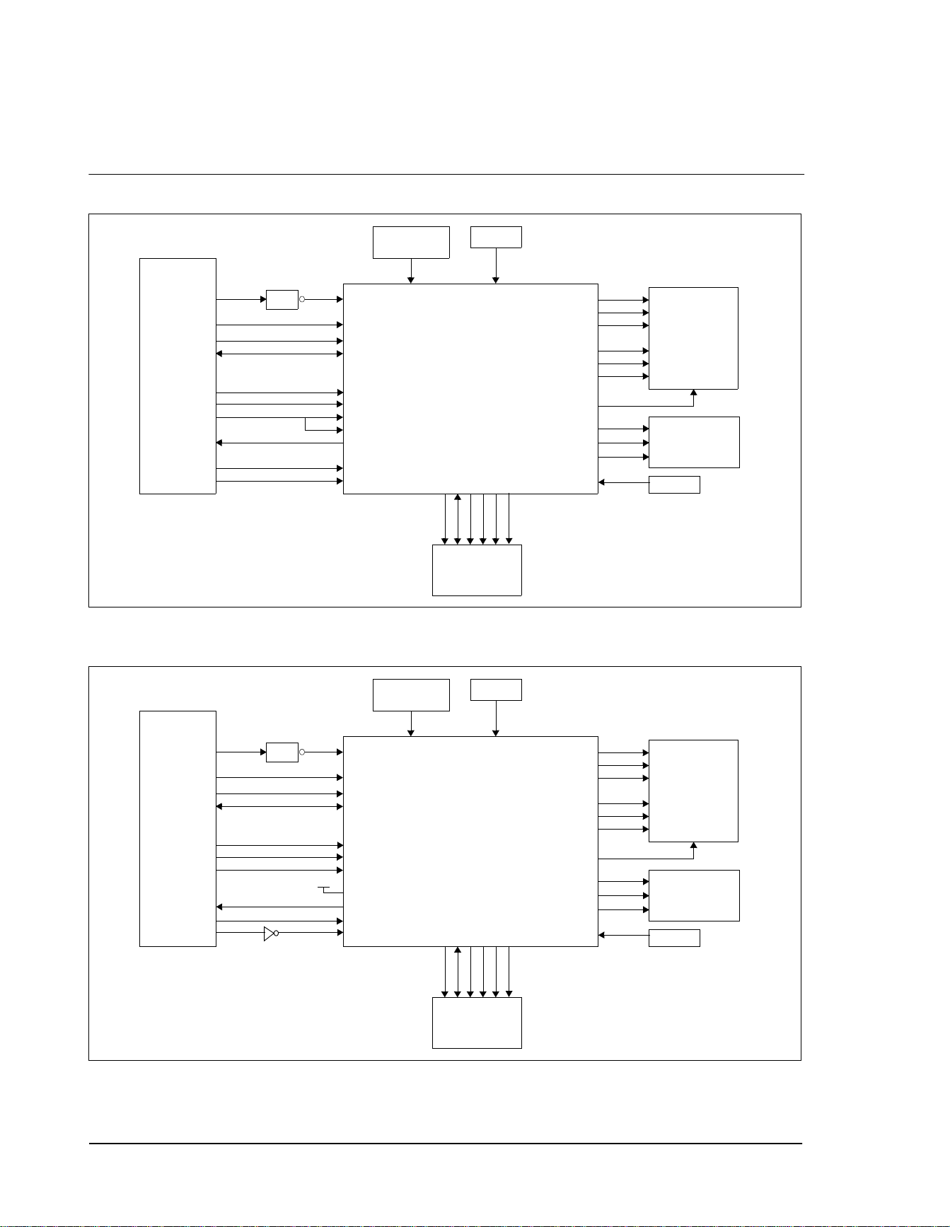
3 Typical System Implementation Diagrams
Figure 3-1: Typical System Diagram (SH-4 Bus)
.
Figure 3-2: Typical System Diagram (SH-3 Bus)
S1D13505F00A
FPFRAME
FPSHIFT
FPLINE
DRDY
FPDAT[15:8]
FPDAT[7:0]
CLKI
Oscillator
FPFRAME
FPSHIFT
FPLINE
MOD
UD[7:0]
LD[7:0]
4/8/16-bit
LCD
Display
SH-4
BUS
RESET#
WE0#
D[15:0]
BS#
RD/WR#
RD#
RDY#
A[20:0]
CKIO
WE0#
RD/WR#
AB[20:0]
DB[15:0]
WE1#
BS#
RD#
M/R#
CS#
BUSCLK
WAIT#
RESET#
A[21]
CSn#
WE1#
LCDPWR
LCAS#
UCAS#
MA[8:0]
MD[15:0]
WE#
RAS#
Power
Management
SUSPEND#
RED,GREEN,BLUE
HRTC
VRTC
CRT
Display
IREF
IREF
WE#
A[8:0]
D[15:0]
RAS#
256Kx16
LCAS#
UCAS#
FPM/EDO-DRAM
S1D13505F00A
FPFRAME
FPSHIFT
FPLINE
DRDY
FPDAT[15:8]
FPDAT[7:0]
CLKI
Oscillator
FPFRAME
FPSHIFT
FPLINE
MOD
UD[7:0]
LD[7:0]
4/8/16-bit
LCD
Display
SH-3
BUS
RESET#
WE0#
D[15:0]
BS#
RD/WR#
RD#
WAIT#
A[20:0]
CKIO
WE0#
RD/WR#
AB[20:0]
DB[15:0]
WE1#
BS#
RD#
M/R#
CS#
BUSCLK
WAIT#
RESET#
A[21]
CSn#
WE1#
LCDPWR
LCAS#
UCAS#
MA[8:0]
MD[15:0]
WE#
RAS#
Power
Management
SUSPEND#
RED,GREEN,BLUE
HRTC
VRTC
CRT
Display
IREF
IREF
WE#
A[8:0]
D[15:0]
RAS#
256Kx16
LCAS#
UCAS#
FPM/EDO-DRAM
Page 21
Page 16
Epson Research and Development
Vancouver Design Center
S1D13505 Hardware Functional Specification
X23A-A-001-14 Issue Date: 01/02/02
.
Figure 3-3: Typical System Diagram (MC6 8K Bus 1, 16-Bit 68000)
.
Figure 3-4: Typical System Diagram (MC6 8K Bus 2, 32-Bit 68030)
S1D13505F00A
FPFRAME
FPSHIFT
FPLINE
DRDY
FPDAT[15:8]
FPDAT[7:0]
CLKI
Oscillator
FPFRAME
FPSHIFT
FPLINE
MOD
UD[7:0]
LD[7:0]
4/8/16-bit
LCD
Display
MC68000
BUS
RESET#
LDS#
D[15:0]
AS#
R/W#
DTACK #
A[20:1]
BCLK
AB0#
RD/WR#
AB[20:1]
DB[15:0]
WE1#
BS#
M/R#
CS#
BUSCLK
WAIT#
RESET#
A[23:21]
FC0, FC1
Decoder
Decoder
UDS#
LCDPWR
LCAS#
UCAS#
MA[8:0]
MD[15:0]
WE#
RAS#
Power
Management
SUSPEND#
RED,GREEN,BLUE
HRTC
VRTC
CRT
Display
IREF
IREF
WE#
A[8:0]
D[15:0]
RAS#
256Kx16
LCAS#
UCAS#
FPM/EDO-DRAM
S1D13505F00A
FPFRAME
FPSHIFT
FPLINE
DRDY
FPDAT[15:8]
FPDAT[7:0]
CLKI
Oscillator
FPFRAME
FPSHIFT
FPLINE
MOD
UD[7:0]
LD[7:0]
4/8/16-bit
LCD
Display
MC68030
BUS
RESET#
SIZ0
D[31:16]
AS#
R/W#
SIZ1
DSACK1#
A[20:0]
BCLK
WE0#
RD/WR#
AB[20:0]
DB[15:0]
WE1#
BS#
RD#
M/R#
CS#
BUSCLK
WAIT#
RESET#
A[31:21]
FC0, FC1
Decoder
Decoder
DS#
LCDPWR
WE#
A[8:0]
D[15:0]
RAS#
256Kx16
LCAS#
UCAS#
MA[8:0]
MD[15:0]
WE#
RAS#
LCAS#
UCAS#
FPM/EDO-DRAM
Power
Management
SUSPEND#
RED,GREEN,BLUE
HRTC
VRTC
CRT
Display
IREF
IREF
Page 22
Epson Research and Development
Page 17
Vancouver Design Center
Hardware Functional Specification S1D13505
Issue Date: 01/02/02 X23A-A-001-14
.
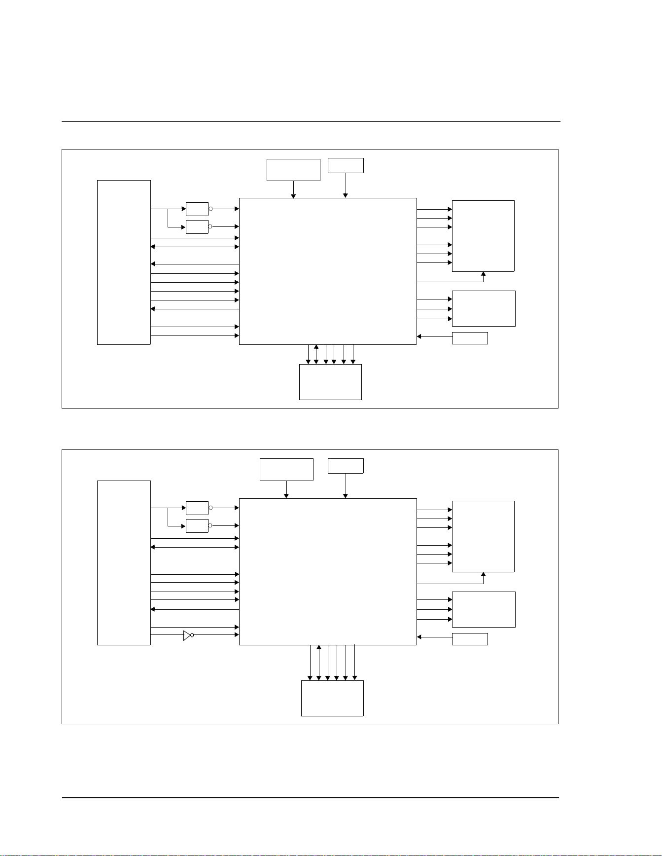
Figure 3-5: Typical System Diagram (Generic Bus)
.
Figure 3-6: Typical System Diagram (NEC VR41xx (M I PS) Bus)
S1D13505F00A
FPFRAME
FPSHIFT
FPLINE
DRDY
FPDAT[15:8]
FPDAT[7:0]
CLKI
Oscillator
FPFRAME
FPSHIFT
FPLINE
MOD
UD[7:0]
LD[7:0]
4/8/16-bit
LCD
Display
Generic
BUS
RESET#
D[15:0]
RD#
WAIT#
A[20:0]
BCLK
RD/WR#
AB[20:0]
DB[15:0]
WE1#
RD#
M/R#
CS#
BUSCLK
WAIT#
RESET#
A[27:21]
CSn#
WE1#
LCDPWR
WE#
A[11:0]
D[15:0]
RAS#
1Mx16
LCAS#
UCAS#
MA[11:0]
MD[15:0]
WE#
RAS#
LCAS#
UCAS#
FPM/EDO-DRAM
Decoder
WE0#
WE0#
Power
Management
SUSPEND#
RED,GREEN,BLUE
HRTC
VRTC
CRT
Display
IREF
IREF
S1D13505F00A
FPFRAME
FPSHIFT
FPLINE
DRDY
FPDAT[15:8]
FPDAT[7:0]
CLKI
Oscillator
FPFRAME
FPSHIFT
FPLINE
MOD
UD[7:0]
LD[7:0]
4/8/16-bit
LCD
Display
MIPS
BUS
RESET
D[15:0]
MEMR#
RDY
A[20:0]
BCLK
RD/WR#
AB[20:0]
DB[15:0]
WE1#
RD#
M/R#
CS#
BUSCLK
WAIT#
RESET#
A[25:21]
CSn#
SBHE#
LCDPWR
WE#
A[11:0]
D[15:0]
RAS#
1Mx16
LCAS#
UCAS#
MA[11:0]
MD[15:0]
WE#
RAS#
LCAS#
UCAS#
FPM/EDO-DRAM
Decoder
WE0#
MEMW#
Power
Management
SUSPEND#
RED,GREEN,BLUE
HRTC
VRTC
CRT
Display
IREF
IREF
VDD
Page 23
Page 18
Epson Research and Development
Vancouver Design Center
S1D13505 Hardware Functional Specification
X23A-A-001-14 Issue Date: 01/02/02
.
Figure 3-7: Typical System Diagram (Philips PR31500/PR31700 Bus)
.
Figure 3-8: Typical System Diagram (Toshiba TX3912 Bus)
S1D13505F00A
FPFRAME
FPSHIFT
FPLINE
DRDY
FPDAT[15:8]
FPDAT[7:0]
CLKI
Oscillator
FPFRAME
FPSHIFT
FPLINE
MOD
UD[7:0]
LD[7:0]
4/8/16-bit
LCD
Display
LCDPWR
WE#
A[11:0]
D[15:0]
RAS#
1Mx16
LCAS#
UCAS#
MA[11:0]
MD[15:0]
WE#
RAS#
LCAS#
UCAS#
FPM/EDO-DRAM
Power
Management
SUSPEND#
RED,GREEN,BLUE
HRTC
VRTC
CRT
Display
IREF
IREF
PR31500
BUS
RESET#
/WE
D[31:16]
/CARDxCSL
/RD
/CARDxWAIT
A[12:0]
DCLKOUT
WE0#
RD/WR#
AB[12:0]
DB[15:0]
WE1#
BS#
RD#
M/R#
CS#
BUSCLK
WAIT#
RESET#
/CARDxCSH
AB[16:13]
ALE
/CARDREG
/CARDIORD
AB20
AB19
AB18
AB17
/CARDIOWR
/PR31700
Philips
S1D13505F00A
FPFRAME
FPSHIFT
FPLINE
DRDY
FPDAT[15:8]
FPDAT[7:0]
CLKI
Oscillator
FPFRAME
FPSHIFT
FPLINE
MOD
UD[7:0]
LD[7:0]
4/8/16-bit
LCD
Display
LCDPWR
WE#
A[11:0]
D[15:0]
RAS#
1Mx16
LCAS#
UCAS#
MA[11:0]
MD[15:0]
WE#
RAS#
LCAS#
UCAS#
FPM/EDO-DRAM
Power
Management
SUSPEND#
RED,GREEN,BLUE
HRTC
VRTC
CRT
Display
IREF
IREF
BUS
RESET#
WE*
D[23:16]
CARDxCSL*
RD*
CARDxWAIT*
A[12:0]
DCLKOUT
WE0#
RD/WR#
AB[12:0]
DB[15:8]
WE1#
BS#
RD#
M/R#
CS#
BUSCLK
WAIT#
RESET#
CARDxCSH*
AB[16:13]
ALE
CARDREG*
CARDIORD*
AB20
AB19
AB18
AB17
CARDIOWR*
Toshiba
TX3912
DB[7:0]
D[31:24]
Page 24
Epson Research and Development
Page 19
Vancouver Design Center
Hardware Functional Specification S1D13505
Issue Date: 01/02/02 X23A-A-001-14
.
Figure 3-9: Typical System Diagram (Power PC Bus)
.
Figure 3-10: Typical System Diagram (PC Card (PCMCIA) Bus)
S1D13505F00A
FPFRAME
FPSHIFT
FPLINE
DRDY
FPDAT[15:8]
FPDAT[7:0]
CLKI
Oscillator
FPFRAME
FPSHIFT
FPLINE
MOD
UD[7:0]
LD[7:0]
4/8/16-bit
LCD
Display
PowerPC
BUS
RESET#
TSIZ1
D[0:15]
TS#
RD/WR#
TSIZ0
TA#
A[11:31]
CLKOUT
WE0#
RD/WR#
AB[20:0]
DB[15:0]
WE1#
BS#
RD#
M/R#
CS#
BUSCLK
WAIT#
RESET#
A[0:10]
Decoder
Decoder
BI#
LCDPWR
WE#
A[8:0]
D[15:0]
RAS#
256Kx16
LCAS#
UCAS#
MA[8:0]
MD[15:0]
WE#
RAS#
LCAS#
UCAS#
FPM/EDO-DRAM
Power
Management
SUSPEND#
RED,GREEN,BLUE
HRTC
VRTC
CRT
Display
IREF
IREF
S1D13505F00A
FPFRAME
FPSHIFT
FPLINE
DRDY
FPDAT[15:8]
FPDAT[7:0]
CLKI
Oscillator
FPFRAME
FPSHIFT
FPLINE
MOD
UD[7:0]
LD[7:0]
4/8/16-bit
LCD
Display
PC Card
BUS
RESET
D[15:0]
-OE
-WAIT
A[20:0]
BCLK
RD/WR#
AB[20:0]
DB[15:0]
WE1#
RD#
M/R#
CS#
BUSCLK
WAIT#
RESET#
A[25:21]
-CE2
LCDPWR
WE#
A[11:0]
D[15:0]
RAS#
1Mx16
LCAS#
UCAS#
MA[11:0]
MD[15:0]
WE#
RAS#
LCAS#
UCAS#
FPM/EDO-DRAM
WE0#
-WE
Power
Management
SUSPEND#
RED,GREEN,BLUE
HRTC
VRTC
CRT
Display
IREF
IREF
Decoder
Decoder
-CE1
Page 25
Page 20
Epson Research and Development
Vancouver Design Center
S1D13505 Hardware Functional Specification
X23A-A-001-14 Issue Date: 01/02/02
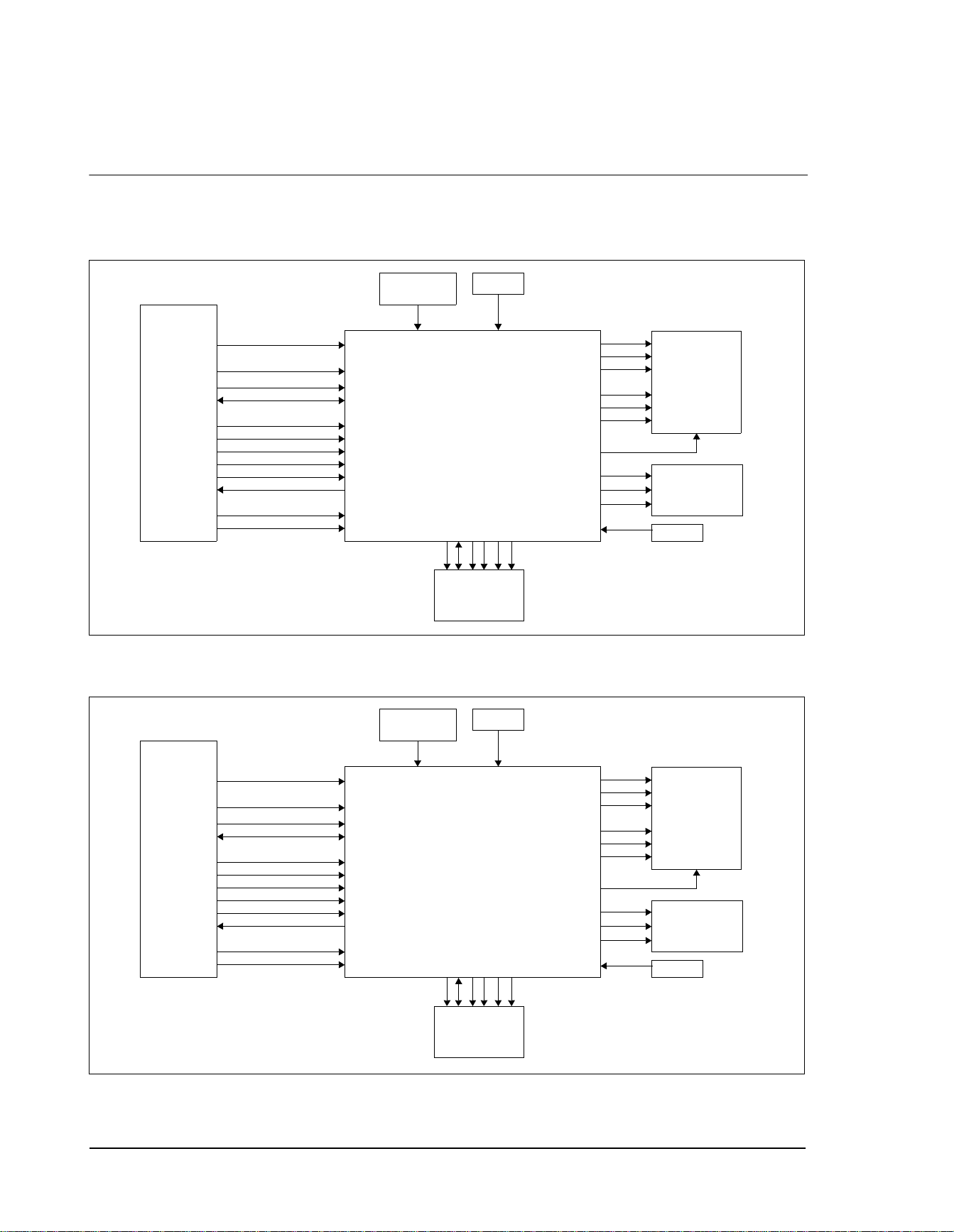
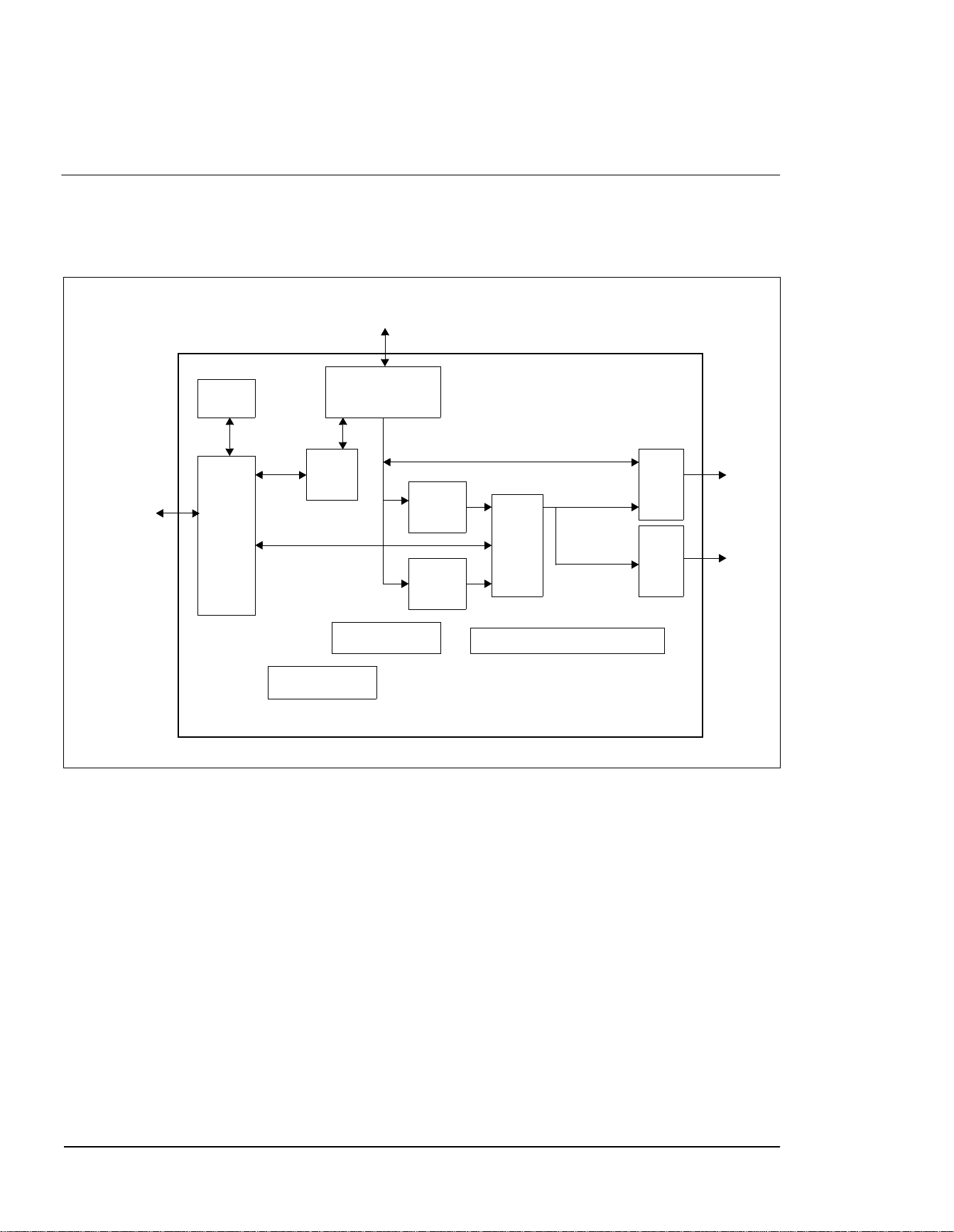
4 Internal Descriptio n
4.1 Block Diagram Showing Datapaths
4.2 Block Descriptions
4.2.1 Register
The Register block contains all the register latches
4.2.2 Host Interface
The Host Interface (I/F) block provides the means for the CPU/MPU to communicate with the
display buffer and internal registers via one of the supported bus interfaces.
4.2.3 CPU R/W
The CPU R/W block synchronizes the CPU requests for display buffer access. If SwivelView is
enabled, the data is rotated in this block.
Clocks
LCD
Memory
Controller
16-bit FPM/EDO-DRAM
LCD
Power Save
Register
CRTC
Look-
I/F
CPU/MPU
Host
I/F
CPU
R/W
Display
FIFO
CRT
Cursor
FIFO
Up
Tables
DAC
Page 26

Epson Research and Development
Page 21
Vancouver Design Center
Hardware Functional Specification S1D13505
Issue Date: 01/02/02 X23A-A-001-14
4.2.4 Memory Controller
The Memory Controller block arbitrates between CPU accesses and display refresh access es as well
as generates the necessary signals to interface to one of th e supported 16-bit memory d evices (FPMDRAM or EDO-DRAM).
4.2.5 Display FIFO
The Display FIFO block fetches display data from the Memory Controller for display refresh.
4.2.6 Cursor FIFO
The Cursor FIFO block fetches Cursor/ink data from the Memory Controller for display refresh.
4.2.7 Look-Up Tables
The Look-Up Tables block contains three 256x4 Look-Up Tables (LUT), one for each primary
color. In monochrome mode, only the green LUT is selected and used. This block contains antisparkle circuitry. The cursor/ink and display data are merged in this block.
4.2.8 CRTC
The CRTC generates the sync timing for the LCD and CRT, defining the vertical and horizontal
display periods.
4.2.9 LCD Interface
The LCD Interface block performs Frame Rate Modulation (FRM) for passive LCD panels and
generates the correct data format and timing control signals for various LCD and TFT/D-TFD
panels.
4.2.10 DAC
The DAC is the Digital to Analog converter for analog CRT support.
4.2.11 Power Save
The Power Save block contains the power save mode circuitry.
4.2.12 Clocks
The Clocks module is the source of all clocks in the chip.
Page 27
Page 22
Epson Research and Development
Vancouver Design Center
S1D13505 Hardware Functional Specification
X23A-A-001-14 Issue Date: 01/02/02
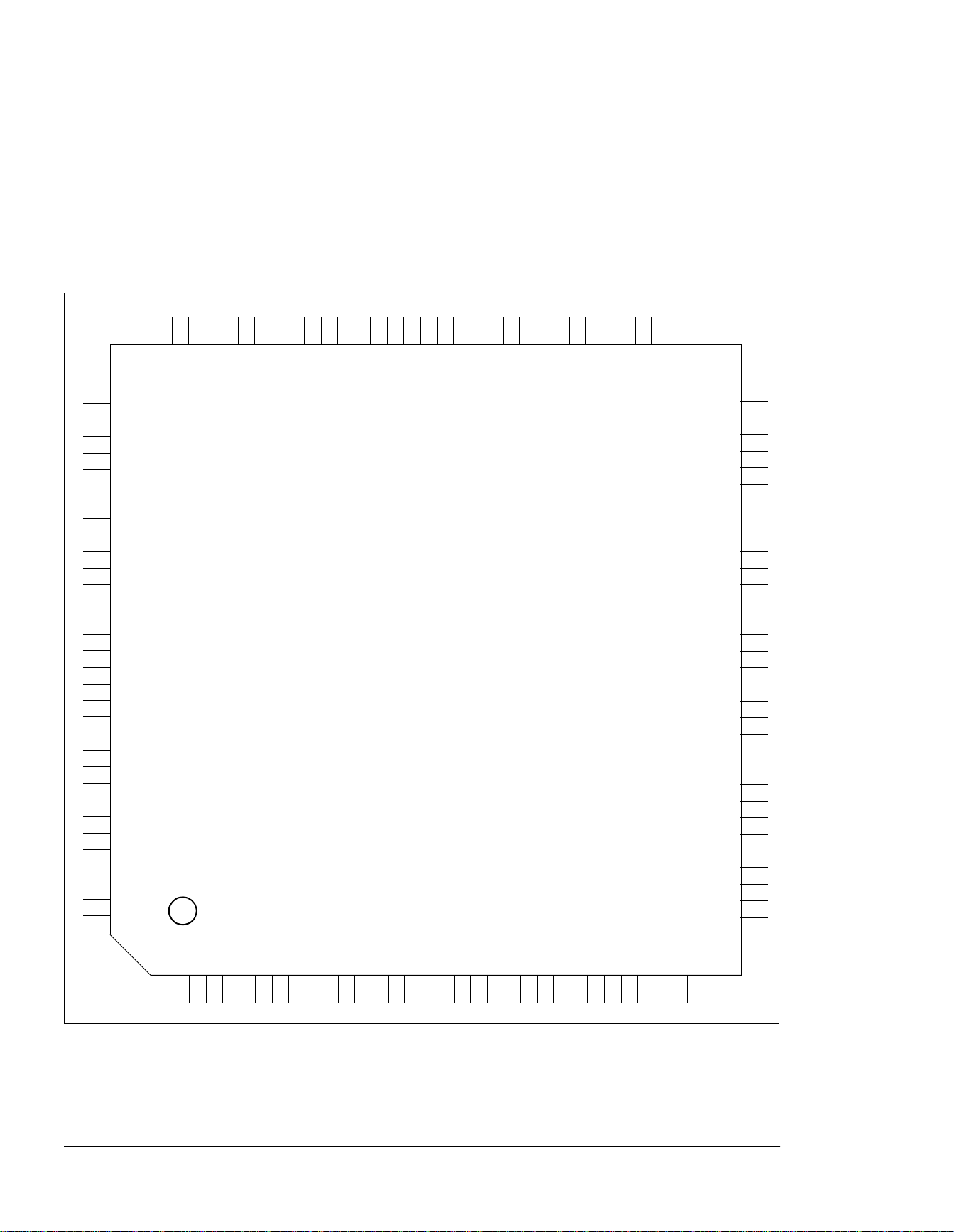
5 Pins
5.1
Pinout Diagram
Figure 5-1: Pinout Diagram
128-pin QFP15 surface mount package
1234567891011121314151617181920212223242526272829303132
96 95 94 93 92 91 90 89 88 87 86 85 84 83 7475 73 72 71 70 69 68 67 66 6582 81 80 79 78 77 76
128
127
126
125
124
123
122
121
120
119
118
117
116
115
114
113
112
111
110
109
108
107
106
105
104
103
102
101
100
99
98
97
33
34
35
36
37
38
39
40
41
42
43
44
45
46
47
48
49
50
58
59
60
61
62
63
51
52
53
54
55
56
57
64
S1D13505
RD/WR#
WAIT#
VDD
VSS
DB15
DB14
DB12
DB8
DB5
DB3
DB2
DB1
DB0
DB13
DB4
AB2
RESET#
VDD
MA6
MA8
DB7
FPDAT3
MA3
MA4
MA2
MA5
MD6
MA11
MA0
MA7
MA10
MA9
VDD
BLUE
VSS
DACVDD
GREEN
FPDAT13
FPDAT10
RAS#
WE#
UCAS#
VSS
MD7
MD8
MD5
MD10
MD4
MD11
MD3
MD12
MD2
MD13
MD1
AB3
BS#
WE1#
WE0#
RD#
M/R#
CS#
AB0
AB1
AB11
AB12
AB15
AB16
AB17
AB18
AB19
AB20
VDD
VSS
DACVSS
IREF
DACVDD
VDD
FPDAT2
FPDAT4
VSS
FPSHIFT
DRDY
LCDPWR
FPLINE
FPFRAME
VSS
MD15
FPDAT15
FPDAT14
VSS
DACVDD
MD14
DB10
DB9
VSS
DB11
DB6
MA1
LCAS#
MD9
FPDAT5
FPDAT7
VDD
TESTEN
FPDAT8
MD0
FPDAT9
FPDAT12
FPDAT0
FPDAT1
VRTC
FPDAT11
HRTC
AB14
AB13
AB7
AB4
AB5
AB8
AB9
AB10
AB6
RED
FPDAT6
CLKI
BUSCLK
SUSPEND#
DACVSS
Page 28
Epson Research and Development
Page 23
Vancouver Design Center
Hardware Functional Specification S1D13505
Issue Date: 01/02/02 X23A-A-001-14
5.2 Pin Descriptio n
Key:
5.2.1 Host Interface
I = Input
O=Output
IO = Bi-Directional (Input/Output)
A=Analog
P=Power pin
C = CMOS level input
CD = CMOS level input with pull down resistor (typical values of 100K
Ω/180ΚΩ
at 5V/3.3V respectively)
CS = CMOS level Schmitt input
COx = CMOS output driver, x denotes driver type (see tables 6-3, 6-4, 6-5 for details)
TSx = Tri-state CMOS output driver, x denotes driver type (see tables 6-3, 6-4, 6-5 for details)
TSxD =
Tri-state CMOS output driver with pull down resistor (typical values of 100K
Ω/180ΚΩ
at 5V/3.3V)
respectively), x denotes driver type (see tables 6-3, 6-4, 6-5 for details)
CNx = CMOS low-noise output driver, x denotes driver type (see tables 6-3, 6-4, 6-5 for details)
Table 5-1: Host Interface Pin Descriptions
Pin Name T yp e Pin # Cell
RESET#
State
Description
AB0 I 3
CS Hi-Z
• For SH-3/SH-4 Bus, this pin inputs system address bit 0 (A0).
• For MC68K Bus 1, this pin inputs the lower data strobe (LDS#).
• For MC68K Bus 2, this pin inputs system address bit 0 (A0).
• For Generic Bus, this pin inputs system address bit 0 (A0).
• For MIPS/ISA Bus, this pin inputs system address bit 0 (SA0).
• For Philips PR31500/31700 Bu s, this pin inputs system address bit 0
(A0).
• For Toshiba TX3912 Bus, this pin inputs system address bit 0 (A0).
• For PowerPC Bus, this pin inputs system address bit 31 (A31).
• For PC Card (PCMCIA) Bus, this pin inputs system address bit 0
(A0).
See
“Host Bus Interface Pin M app ing ”
for summary. See th e re spe ct ive
AC Timing diagram for detailed functionality.
AB[12:1] I
119-128,
1, 2
CHi-Z
• For PowerPC Bus, these pins input the system address bits 19
through 30 (A[19:30]).
• For all other busses, these pins input the system address bits 12
through 1 (A[12:1]).
See
“Host Bus Interface Pin M app ing ”
for summary. See th e re spe ct ive
AC Timing diagram for detailed functionality.
Page 29

Page 24
Epson Research and Development
Vancouver Design Center
S1D13505 Hardware Functional Specification
X23A-A-001-14 Issue Date: 01/02/02
AB[16:13] I 115-118
CHi-Z
• For Philips PR31500/31700 Bus, these pins are connected to V
DD
.
• For Toshiba TX3912 Bus, these pins are connected to VDD.
• For PowerPC Bus, these pins input the system address bits 15
through 18 (A[15:18]).
• For all other busses, these pins input the system address bits 16
through 13 (A[16:13]).
See
“Host Bus Interface Pin Mapping”
for summary. See the respective
AC Timing diagram for detailed functionality.
AB17 I 114
CHi-Z
• For Philips PR31500/31700 Bus, this pin inputs the IO write
command (/CARDIOWR).
• For Toshiba TX3912 Bus, this pin inputs the IO write command
(CARDIOWR*).
• For PowerPC Bus, this pin inputs the system address bit 14 (A14).
• For all other busses, this pin inputs the system address bit 17 (A17).
See
“Host Bus Interface Pin Mapping”
for summary. See the respective
AC Timing diagram for detailed functionality.
AB18 I 113
CHi-Z
• For Philips PR31500/31700 Bus, this pin inputs the IO read
command (/CARDIORD).
• For Toshiba TX3912 Bus, this pin inputs the IO read command
(CARDIORD*).
• For PowerPC Bus, this pin inputs the system address bit 13 (A13).
• For all other busses, this pin inputs the system address bit 18 (A18).
See
“Host Bus Interface Pin Mapping”
for summary. See the respective
AC Timing diagram for detailed functionality.
AB19 I 112
CHi-Z
• For Philips PR31500/31700 Bus, this pin inputs the card control
register access (/CARDREG).
• For Toshiba TX3912 Bus, this pin inputs the card control register
(CARDREG*).
• For PowerPC Bus, this pin inputs the system address bit 12 (A12).
• For all other busses, this pin inputs the system address bit 19 (A19).
See
“Host Bus Interface Pin Mapping”
for summary. See the respective
AC Timing diagram for detailed functionality.
AB20 I 111
CHi-Z
• For the MIPS/ISA Bus, this pin inputs system address bit 20. Note
that for the ISA Bus, the unlatched LA20 must first be latched before
input to AB20.
• For Philips PR31500/31700 Bus, this pin inputs the address latch
enable (ALE).
• For Toshiba TX3912 Bus, this pin inputs the address latch enable
(ALE).
• For PowerPC Bus, this pin inputs the system address bit 11 (A11).
• For all other busses, this pin inputs the system address bit 20 (A20).
See
“Host Bus Interface Pin Mapping”
for summary. See the respective
AC Timing diagram for detailed functionality.
Table 5-1: Host Interface Pin Descriptions (Continued)
Pin Name Type Pin # Cell
RESET#
State
Description
Page 30
Epson Research and Development
Page 25
Vancouver Design Center
Hardware Functional Specification S1D13505
Issue Date: 01/02/02 X23A-A-001-14
DB[15:0] IO 16-31
C/TS2 Hi-Z
These pins are the system data bus. For 8-bit bus modes, unused data
pins should be tied to VDD.
• For SH-3/SH-4 Bus, these pins are connected to D[15:0].
• For MC68K Bus 1, these pins are connected to D[15:0].
• For MC68K Bus 2, these pins are connected to D[31:16] for 32-bit
devices (e.g. MC68030) or D[15:0 ] for 16-bit devices (e.g. M C68 340 ).
• For Generic Bus, these pins are connected to D[15:0].
• For MIPS/ISA Bus, these pins are connected to SD[15:0].
• For Philips PR31500/31700 Bus, these pins are connected to
D[31:16].
• For Toshiba TX3912 Bus, pins [15:8] are connected to D[23:16] and
pins [7:0] are connected to D[31:24].
• For PowerPC Bus, these pins are connected to D[0:15].
• For PC Card (PCMCIA) Bus, these pins are connected to D[15:0].
See
“Host Bus Interface Pin M app ing ”
for summary. See th e re spe ct ive
AC Timing diagram for detailed functionality.
WE1# IO 9
CS/TS
2
Hi-Z
This is a multi-purpose pin:
• For SH-3/SH-4 Bus, this pin inputs the write enable signal for the
upper data byte (WE1#).
• For MC68K Bus 1, this pin inputs the upper data strobe (UDS#).
• For MC68K Bus 2, this pin inputs the data strobe (DS#).
• For Generic Bus, this pin inputs the write enable signal for the upper
data byte (WE1#).
• For MIPS/ISA Bus, this pin inputs the syste m by te high ena b le sign al
(SBHE#).
• For Philips PR31500/31700 Bus, this pin inputs the odd byte access
enable signal (/CARDxCSH).
• For Toshiba TX3912 Bus, this pin inputs the odd byte access enable
signal (CARDxCSH*).
• For PowerPC Bus, this pin outputs the burst inhibit signal (BI#).
• For PC Card (PCMCIA) Bus, this pin inputs the card enable 2 signal
(-CE2).
See
“Host Bus Interface Pin M app ing ”
for summary. See th e re spe ct ive
AC Timing diagram for detailed functionality.
M/R# I 5 C
Hi-Z
• For Philips PR31500/31700 Bus, this pin is connected to V
DD
.
• For Toshiba TX3912 Bus, this pin is connected to V
DD
.
• For all other busses, this input pin is used to select between the
display buffer and register address spa ces o f the S1 D13505. M/R# is
set high to access the display buffer and low to access the registers.
See
Register Mapping
.
See Table 5-6:, “CPU Interface Pin Mapping,” on page 34.
CS# I 4
CHi-Z
• For Philips PR31500/31700 Bus, this pin is connected to V
DD
.
• For Toshiba TX3912 Bus, this pin is connected to V
DD
.
• For all other busses, this is the Chip Select input.
See Table 5-6:, “CPU Interface Pin Mapping,” on page 34. See the
respective AC Timing diagram for detailed functionality.
Table 5-1: Host Interface Pin Descriptions (Continued)
Pin Name T yp e Pin # Cell
RESET#
State
Description
Page 31

Page 26
Epson Research and Development
Vancouver Design Center
S1D13505 Hardware Functional Specification
X23A-A-001-14 Issue Date: 01/02/02
BUSCLK I 13
CHi-Z
This pin inputs the system bus clock. It is possible to apply a 2x clock
and divide it by 2 internally - see MD12 in
Summary of Configuration
Options
.
• For SH-3/SH-4 Bus, this pin is connected to CKIO.
• For MC68K Bus 1, this pin is connected to CLK.
• For MC68K Bus 2, this pin is connected to CLK.
• For Generic Bus, this pin is connected to BCLK.
• For MIPS/ISA Bus, this pin is connected to CLK.
• For Philips PR31500/31700 Bus, this pin is connected to DCLKOUT.
• For Toshiba TX3912 Bus, this pin is connected to DCLKOUT.
• For PowerPC Bus, this pin is connected to CLKOUT.
• For PC Card (PCMCIA) Bus, this pin is connected to CLKI.
See
“Host Bus Interface Pin Mapping”
for summary. See the respective
AC Timing diagram for detailed functionality.
BS# I 6
CS Hi-Z
This is a multi-purpose pin:
• For SH-3/SH-4 Bus, this pin inputs the bus start signal (BS#).
• For MC68K Bus 1, this pin inputs the address strobe (AS#).
• For MC68K Bus 2, this pin inputs the address strobe (AS#).
• For Generic Bus, this pin is connected to V
DD
.
• For MIPS/ISA Bus, this pin is connected to V
DD
.
• For Philips PR31500/31700 Bus, this pin is connected to VDD.
• For Toshiba TX3912 Bus, this pin is connected to VDD.
• For PowerPC Bus, this pin inputs the Transfer Start signal (TS#).
• For PC Card (PCMCIA) Bus, this pin is connected to V
DD
.
See
“Host Bus Interface Pin Mapping”
for summary. See the respective
AC Timing diagram for detailed functionality.
RD/WR# I 10
CS Hi-Z
This is a multi-purpose pin:
• For SH-3/SH-4 Bus, this pin inputs the read write signal (RD/WR#).
The S1D13505 needs this signal for early decode of the bus cycle.
• For MC68K Bus 1, this pin inputs the read write signal (R/W#).
• For MC68K Bus 2, this pin inputs the read write signal (R/W#).
• For Generic Bus, this pin input s the read comman d for the upp er data
byte (RD1#).
• For MIPS/ISA Bus, this pin is connected to V
DD
.
• For Philips PR31500/31700 Bus, this pin input s the even byte access
enable signal (/CARDxCSL).
• For Toshiba TX3912 Bus, this p in in puts t he even byte access enab l e
signal (CARDxCSL*).
• For PowerPC Bus, this pin inputs the read write signal (RD/WR#).
• For PC Card (PCMCIA) Bus, this pin inputs the card enable 1 signal
(-CE1).
See
“Host Bus Interface Pin Mapping”
for summary. See the respective
AC Timing diagram for detailed functionality.
Table 5-1: Host Interface Pin Descriptions (Continued)
Pin Name Type Pin # Cell
RESET#
State
Description
Page 32

Epson Research and Development
Page 27
Vancouver Design Center
Hardware Functional Specification S1D13505
Issue Date: 01/02/02 X23A-A-001-14
RD# I 7
CS Hi-Z
This is a multi-purpose pin:
• For SH-3/SH-4 Bus, this pin inputs the read signal (RD#).
• For MC68K Bus 1, this pin is connected to V
DD
.
• For MC68K Bus 2, this pin inputs the bus size bit 1 (SIZ1).
• For Generic Bus, this pin inputs the read comma nd f or the low er data
byte (RD0#).
• For MIPS/ISA Bus, this pin inputs the memory read signal (MEMR#).
• For Philips PR31500/31700 Bus, this pin inputs the memory read
command (/RD).
• For Toshiba TX3912 Bus, this pin inputs the mem ory read command
(RD*).
• For PowerPC Bus, this pin inputs the transfer size 0 signal (TSIZ0).
• For PC Card (PCMCIA) Bus, this pin inputs the output enab le si gna l
(-OE).
See
“Host Bus Interface Pin M app ing ”
for summary. See th e re spe ct ive
AC Timing diagram for detailed functionality.
WE0# I 8
CS Hi-Z
This is a multi-purpose pin:
• For SH-3/SH-4 Bus, this pin inputs the write enable signal for the
lower data byte (WE0#).
• For MC68K Bus 1, this pin must be connected to V
DD
• For MC68K Bus 2, this pin inputs the bus size bit 0 (SIZ0).
• For Generic Bus, this pin inputs the write enable signal for the lower
data byte (WE0#).
• For MIPS/ISA Bus, this pin inputs the memory write signal
(MEMW#).
• For Philips PR31500/31700 Bus, this pin inputs the memory write
command (/WE).
• For Toshiba TX3912 Bus, this pi n i nputs the memory write command
(WE*).
• For PowerPC Bus, this pin inputs the Trans fer Size 1 signal (TSIZ1).
• For PC Card (PCMCIA) Bus, this pin inputs the write enable signal (WE).
See
“Host Bus Interface Pin M app ing ”
for summary. See th e re spe ct ive
AC Timing diagram for detailed functionality.
Table 5-1: Host Interface Pin Descriptions (Continued)
Pin Name T yp e Pin # Cell
RESET#
State
Description
Page 33

Page 28
Epson Research and Development
Vancouver Design Center
S1D13505 Hardware Functional Specification
X23A-A-001-14 Issue Date: 01/02/02
WAIT# O 15
TS2 Hi-Z
The active polarity of the WAIT # output is configurab le; the state of MD5
on the rising edge of RESET# defines the active pol arity of WAIT# - see
“Summary of Configuration Options”
.
• For SH-3 Bus, this pin o utputs the wait request signal (WAIT#); MD5
must be pulled low during reset by the internal pull-down resistor.
• For SH-4 Bus, this pin outputs th e ready sig nal (RDY#); MD5 must be
pulled high during reset by an external pull-up resistor.
• For MC68K Bus 1, this pin outputs the data transfer acknowledge
signal (DTACK#); MD5 must be pulled high during reset by an
external pull-up resistor.
• For MC68K Bus 2, this pin outputs the data transfer and size
acknowled ge bit 1 (DSA CK1#); M D5 mu st be pu lled hig h during rese t
by an external pull-up resistor.
• For Generic Bus, this pin output s the wait signal (WAIT#); MD5 must
be pulled low during reset by the internal pull-down resistor.
• For MIPS/ISA Bus, this pin outputs the IO channel ready signal
(IOCHRDY); MD5 must be pulled low during res et b y the internal pulldown resistor.
• For Philips PR31500/31700 Bus, this pin outpu ts the wait state si gnal
(/CARDxWAIT); MD5 must be pulled low during reset by the internal
pull-down resistor.
• For Toshiba TX3912 Bus, this pin outputs the wait state signal
(CARDxWAIT*); MD5 must be pulled low during reset by the internal
pull-down resistor.
• For PowerPC Bus, this pin outputs the transfer acknowledge signal
(TA#); MD5 must be pulled high during reset by an external pull-up
resistor.
• For PC Card (PCMCIA) Bus, this pin outputs the wait sign al (-WAIT);
MD5 must be pulled low during reset by the internal pull-down
resistor.
See
“Host Bus Interface Pin Mapping”
for summary. See the respective
AC Timing diagram for detailed functionality.
RESET# I 11
CS 0
Active low input tha t clea rs all intern al reg ist ers an d force s all ou tpu ts to
their inactive states. Note that active high RESET signals must be
inverted before input to this pin.
Table 5-1: Host Interface Pin Descriptions (Continued)
Pin Name Type Pin # Cell
RESET#
State
Description
Page 34

Epson Research and Development
Page 29
Vancouver Design Center
Hardware Functional Specification S1D13505
Issue Date: 01/02/02 X23A-A-001-14
5.2.2 Memory Interface
Table 5-2: Memory I nterface Pin Descriptions
Pin Name Type Pin # Cell
RESET#
State
Description
LCAS# O 51 CO1 1
• For dual-CAS# DRAM, this is the column address strobe for the
lower byte (LCAS#).
• For single-CAS# DRAM, this is the column address strobe (CAS#).
See
“Memory Interface Pin Mapping”
for summary. See
Memory
Interface Timing
for detailed functionality.
UCAS# O 52 CO1 1
This is a multi-purpose pin:
• For dual-CAS# DRAM, this is the column address strobe for the
upper byte (UCAS#).
• For single-CAS# DRAM, this is the write enable signal for the upper
byte (UWE#).
See
“Memory Interface Pin Mapping”
for summary. See
Memory
Interface Timing
for detailed functionality.
WE# O 53 CO1 1
• For dual-CAS# DRAM, this is the write enable signal (WE#).
• For single-CAS# DRAM, this is the write enable signal for the lower
byte (LWE#).
See
“Memory Interface Pin Mapping”
for summary. See
Memory
Interface Timing
for detailed functionality.
RAS# O 54 CO1 1
Row address strobe - see
Memory Interfa ce Timing
for detailed
functionality.
MD[15:0] IO
34, 36, 38,
40, 42, 44,
46, 48, 49,
47, 45, 43,
41, 39, 37,
35
C/TS
1D
Hi-Z
Bi-Directional memory data bus.
During reset, these pins are i nputs an d their s tates at th e risin g edge of
RESET# are used to configure the chip - see
Summary of
Configuration Options
. Internal pull-down resistors (typical values of
100K
Ω/180ΚΩ
at 5V/3.3V respectively) pull the reset states to 0.
External pull-up resistors can be used to pull the reset states to 1.
See
Memory Inter face Timing
for detailed functionality.
Page 35

Page 30
Epson Research and Development
Vancouver Design Center
S1D13505 Hardware Functional Specification
X23A-A-001-14 Issue Date: 01/02/02
MA[8:0] O
58, 60, 62,
64, 66, 67,
65, 63, 61
CO1 0utput
Multiplexed memory address - see
Memory Interface Timing
for
functionality.
MA9 IO 56
C/TS
1
0utput
This is a multi-purpose pin:
• For 2M byte DRAM, this is memory address bit 9 (MA9).
• For asymmetrical 512K byte DRAM, this is memory address bit 9
(MA9).
• For symmetrical 512K byte DRAM, this pin can be used as general
purpose IO pin 3 (GPIO3).
Note that unless configured otherwise, this pin defaults to an input and
must be driven to a valid logic level.
See
“Memory Interface Pin Mapping”
for summary. See
Memory
Interface Timing
for detailed functionality.
MA10 IO 59
C/TS
1
0utput
This is a multi-purpose pin:
• For asymmetrical 2M byte DRAM this is memory address bit 10
(MA10).
• For symmetrical 2M byte DRAM and all 512K byte DRAM this pin
can be used as general purpose IO pin 1 (GPIO1).
Note that unless configured otherwise, this pin defaults to an input and
must be driven to a valid logic level.
See
“Memory Interface Pin Mapping”
for summary. See
Memory
Interface Timing
for detailed functionality.
MA11 IO 57
C/TS
1
0utput
This is a multi-purpose pin:
• For asymmetrical 2M byte DRAM this is memory address bit 11
(MA11).
• For symmetrical 2M byte DRAM and all 512K byte DRAM this pin
can be used as general purpose IO pin 2 (GPIO2).
Note that unless configured otherwise, this pin defaults to an input and
must be driven to a valid logic level.
See
“Memory Interface Pin Mapping”
for summary. See
Memory
Interface Timing
for detailed functionality.
Table 5-2: Memory Interfa c e Pin D esc r ip tio ns (Con tin ue d)
Pin Name Type Pin # Cell
RESET#
State
Description
Page 36

Epson Research and Development
Page 31
Vancouver Design Center
Hardware Functional Specification S1D13505
Issue Date: 01/02/02 X23A-A-001-14
5.2.3 LCD Interface
5.2.4 CRT Interface
Table 5-2: LCD
Interface Pin Descriptions
Pin Name Type Pin # Cell RESET# State Description
FPDAT[15:0] O
95-88,
86-79
CN3 0utput
Panel data bus. Not all pins are used for some panels - see
LCD
Interface Pin Mapping
for details. Unused pins are driven low.
FPFRAME O 73 CN3 0utput Frame pulse
FPLINE O 74 CN3 0utput Line pulse
FPSHIFT O 77 CO3 0utput Shift clock
LCDPWR O 75 CO1
0utput if
MD[10]=0
1 if MD[10]=1
LCD power control out put. The a ctive polarit y of this output i s sele cted
by the state of MD10 at the rising edge of RESET# - see
Summary of
Configuration Options
. This output is controlled by the power save
mode circuitry - see
Power Save Modes
for details.
DRDY O 76 CN3 0utput
This is a multi-purpose pin:
• For TFT/D-TFD panels this is the display enable output (DRDY).
• For passive LCD with Format 1 interface this is the 2nd Shift Clock
(FPSHIFT2)
• For all other LCD panels this is the LCD backplane bias signal
(MOD).
See
LCD Interface Pin Mapping
and REG[02h] for details.
Table 5-3: CRT Interface Pin Descriptions
Pin Name Type Pin # Cell
RESET
# State
Description
HRTC IO 107 CN3 0utput Horizontal retrace signal for CRT
VRTC IO 108 CN3 0utput Vertical retrace signal for CRT
RED O 100 A Analog output for CRT color Red
GREEN O 103 A Analog output for CRT color Green
BLUE O 105 A Analog output for CRT color Blue
IREF I 101 A
Current reference for DAC - see
Analog Pins
. This pin must be left
unconnected if the DAC is not needed.
Page 37

Page 32
Epson Research and Development
Vancouver Design Center
S1D13505 Hardware Functional Specification
X23A-A-001-14 Issue Date: 01/02/02
5.2.5 Miscellaneous
Table 5-4: Miscellaneous Interface Pin Descriptions
Pin Name Type Pin # Cell RESET# State Description
SUSPEND# IO 71 CS/TS1
Hi-Z if MD[9]=0
High if
MD[10:9]=01
Low if
MD[10:9]=11
This pin can be used as a power-down input (SUSPEND#)
or as an output possibly used for controlling the LCD
backlight power:
• When MD9 = 0 at rising edge of RESET#, this pin is an
active-low Schmitt input used to put the S1D13505 into
Hardware Suspend mode - see Section 15, “Power Save
Modes” for details.
• When MD[10:9] = 01 at rising edge of RESET#, this pin
is an output (GPO) with a reset s ta te of 1. Th e s tate of G PO
is controlled by REG[21h] bit 7.
• When MD[10:9] = 11 at rising edge of RESET#, this pin
is an output (GPO) with a reset s ta te of 0. Th e s tate of G PO
is controlled by REG[21h] bit 7.
CLKI I 69 C
Input clock for the internal pixel clock (PCLK) and memory
clock (MCLK). PCLK and MC LK are derived from CLKI - see
REG[19h] for details.
TESTEN I 70 CD Hi-Z
Test Enable. This pin should be connected to V
SS
for normal
operation.
VDD P
12, 33, 55, 72,
97, 109
PV
DD
DACVDD P 99, 102, 104 P DAC V
DD
VSS P
14, 32, 50, 68,
78, 87, 96, 110
PV
SS
DACVSS P 98, 106 P DAC V
SS
Page 38

Epson Research and Development
Page 33
Vancouver Design Center
Hardware Functional Specification S1D13505
Issue Date: 01/02/02 X23A-A-001-14
5.3 Summary of Configuration Options
Table 5-5: Summary of Power On/Reset Options
Pin Name value on this pin at rising edge of RESET# is used to configure:
(1/0)
10
MD0 8-bit host bus interface 16-bit host bus interface
MD[3:1]
Select host bus interface:MD[11] = 0:
000 = SH-3/SH-4 bus interface
001 = MC68K Bus 1
010 = MC68K Bus 2
011 = Generic
100 = Reserved
101 = MIPS/ISA
110 = PowerPC
111 = PC Card (when MD11 = 1 Philips PR31500/PR31700 or Toshiba TX3912 Bus)
MD4 Little Endian Big Endian
MD5 WAIT# is active high (1 = insert wait state) WAIT# is active low (0 = insert wait state)
MD[7:6]
Memory Address/GPIO confi gur atio n:
00 = symmetrical 256K×16 DRAM. MA[8:0] = DRAM address. MA[11:9] = GPIO2,1,3 pins.
01 = symmetrical 1M×16 DRAM. MA[9:0] = DRAM address. MA[10:11] = GPIO2,1 pins.
10 = asymmetrical 256K×16 DRAM. MA[9:0] = DRAM address. MA[10:11] = GPIO2,1 pins.
11 = asymmet rical 1M×16 DRAM. MA[11:0] = DRAM address.
MD8 Not used
MD9 SUSPEND# pin configured as GPO output SUSPEND# pin configured as SUSPEND# input
MD10
Active low LCDPWR polarity or
active high GPO polarity
Active high LCDPWR polarity or
active low GPO polarity
MD11 Alternate Host Bus Interface Selected Primary Host Bus Interface Selected
MD12 BUSCLK input divided by 2 BUSCLK input not divided
MD[15:13] Not used
Page 39

Page 34
Epson Research and Development
Vancouver Design Center
S1D13505 Hardware Functional Specification
X23A-A-001-14 Issue Date: 01/02/02
5.4 Multiple Function Pin Mapping
Note
1
The bus signal A0 is not used by the S1D13505 internally.
Table 5-6: CPU Interf a ce Pin Mapping
S1D1350
5
Pin
Names
SH-3 SH-4
MC68K
Bus 1
MC68K
Bus 2
Generic MIPS/ISA
Philips
PR31500
/PR31700
Toshiba
TX3912
PowerPC
PC Card
(PCMCIA)
AB20 A20 A20 A20 A20 A20 LatchA20 ALE ALE A11 A20
AB19 A19 A19 A19 A19 A19 SA19 /CARDREG CARDREG* A12 A19
AB18 A18 A18 A18 A18 A18 SA18 /CARDIORD CARDIORD* A13 A18
AB17 A17 A17 A17 A17 A17 SA17 /CARDIOWR CARDIOWR* A14 A17
AB[16:13] A[16:13] A[16:13] A[16:13] A[16:13] A[16:13] SA[16:13] V
DD
V
DD
A[15:18] A[16:13]
AB[12:1] A[12:1] A[12:1] A[12:1] A[12:1] A[1 2:1] SA[12:1] A[12:1] A[12:1] A[19:30] A[12:1]
AB0 A0
1
A0 LDS# A0 A0
1
SA0 A0
1
A0
1
A31 A0
1
DB[15:8] D[15:8] D[15:8] D[15:8] D[31:24] D[15:8] SD[15:8] D[31:24] D[31:24] D[0:7] D[15:8]
DB[7:0] D[7:0] D[7:0] D[7:0] D[23:16] D[7:0] SD[7:0] D[23:16] D[23:16] D[8:15 D[7:0]
WE1# WE1# WE1# UDS# DS# WE1# SBHE# /CARDxCSH C ARDxCSH* BI# -CE2
M/R# External Decode V
DD
External Decode
CS# External Decode V
DD
External Decode
BUSCLK CKIO CKIO CLK CLK BCLK CLK DCLKOUT DCLKOUT CLKOUT CLKI
BS# BS# BS# AS# AS# V
DD
V
DD
V
DD
V
DD
TS# V
DD
RD/WR# RD/WR# RD/WR# R/W# R/W# RD1# V
DD
/CARDxCSL CARDxCSL* RD/WR# -CE1
RD# RD# RD# V
DD
SIZ1 RD0# MEMR# /RD RD* TSIZ0 -OE
WE0# WE0# WE0# V
DD
SIZ0 WE0# MEMW# /WE WE* TSIZ1 -WE
WAIT# WAIT# RDY DTACK# DSACK1# WAIT# IOCHRDY /CARDxWAIT CARDxWAIT* TA# -WAIT
RESET# RESET# RESET# RESET# RESET# RESET#
inverted
RESET
RESET# PON* RESET#
inverted
RESET
Page 40

Epson Research and Development
Page 35
Vancouver Design Center
Hardware Functional Specification S1D13505
Issue Date: 01/02/02 X23A-A-001-14
Note
All GPIO pins default to input on reset an d unless programmed o therwise, should be conn ected
to either V
SS
or IO VDD if not used.
Table 5-7: Memory Interface Pin Mapping
S1D13505
Pin Names
FPM/EDO-DRAM
Sym 256Kx16 Asym 256Kx16 Sym 1Mx16 Asym 1Mx16
2-CAS# 2-WE# 2-CAS# 2-WE# 2-CAS# 2-WE# 2-CAS# 2-WE#
MD[15:0] D[15:0]
MA[8:0] A[8:0]
MA9 GPIO3 A9 A9
MA10 GPIO1 A10
MA11 GPIO2 A11
UCAS# UCAS# UWE# UCAS# UWE# UCAS# UWE# UCAS# UWE#
LCAS# LCAS# CAS# LCAS# CAS# LCAS# CAS# LCAS# CAS#
WE# WE# LWE# WE# LWE# WE# LWE# WE# LWE#
RAS# RAS#
Page 41

Page 36
Epson Research and Development
Vancouver Design Center
S1D13505 Hardware Functional Specification
X23A-A-001-14 Issue Date: 01/02/02
Table 5-8: LCD Interface Pin Mapping
S1D13505
Pin
Names
Monochrome Passive
Panel
Color Passive Panel
Color TFT/D-TFD Panel
Single Dual Single
Single
Format 1
Single
Format 2
Single Dual
4-bit 8-bit 8-bit 4-bit 8-bit 8-bit 16-Bit 8-bit 16-bi t 9-bit 12-bit 18-bit
FPFRAME FPFRAME
FPLINE FPLINE
FPSHIFT FPSHIFT
DRDY MOD
FPSHIFT
2
MOD DRDY
FPDAT0
driven 0 D0 LD0 driven 0 D0 D0 D0 LD0 LD0 R2 R3 R5
FPDAT1
driven 0 D1 LD1 driven 0 D1 D1 D1 LD1 LD1 R1 R2 R4
FPDAT2 driven 0 D2 LD2 driven 0 D2 D2 D2 LD2 LD2 R0 R1 R3
FPDAT3
driven 0 D3 LD3 driven 0 D3 D3 D3 LD3 LD3 G2 G3 G5
FPDAT4 D0 D4 UD0 D0 D4 D4 D4 UD0 UD0 G1 G2 G4
FPDAT5 D1 D5 UD1 D1 D5 D5 D5 UD1 UD1 G0 G1 G3
FPDAT6 D2 D6 UD2 D2 D6 D6 D6 UD2 UD2 B2 B3 B5
FPDAT7 D3 D7 UD3 D3 D7 D7 D7 UD3 UD3 B1 B2 B4
FPDAT8
driven 0 driven 0 driven 0 driven 0 driven 0 driven 0 D8 driven 0 LD4 B0 B1 B3
FPDAT9 driven 0 driven 0 driven 0 driven 0 driven 0 driven 0 D9 driven 0 LD5 driven 0 R0 R2
FPDAT10
driven 0 driven 0 driven 0 driven 0 driven 0 driven 0 D10 driven 0 LD6 driven 0 driven 0 R1
FPDAT11 driven 0 driven 0 driven 0 driven 0 driven 0 driven 0 D11 driven 0 LD7 driven 0 G0 G2
FPDAT12] driven 0 driven 0 driven 0 driven 0 driven 0 driven 0 D12 driven 0 UD4 driven 0 driven 0 G1
FPDAT13 driven 0 driven 0 driven 0 driven 0 driven 0 driven 0 D13 driven 0 UD5 driven 0 driven 0 G0
FPDAT14
driven 0 driven 0 driven 0 driven 0 driven 0 driven 0 D14 driven 0 UD6 driven 0 B0 B2
FPDAT15 driven 0 driven 0 driven 0 driven 0 driven 0 driven 0 D15 driven 0 UD7 driven 0 driven 0 B1
Page 42

Epson Research and Development
Page 37
Vancouver Design Center
Hardware Functional Specification S1D13505
Issue Date: 01/02/02 X23A-A-001-14
5.5 CRT Interface
The following figure shows the external circuitry for the CRT interface.
Figure 5-3: External C ircuitry for CRT Interface
2N2222
4.6 mA
4.6 mA
140
Ω
1%
1k
Ω
1%
1.5k
Ω
1%
DAC VSSDAC V
SS
V+
R
V-
DAC V
SS
DAC V
SS
DAC VDD = 2.7V to 5.5V
DAC V
DD
= 3.3V
LM334
290
Ω
1%
29
Ω
1%
1N457
1µF
150
Ω
1%
150
Ω
1%
150
Ω
1%
DAC VSSDAC V
SS
DAC V
SS
4.6 mA
OR
IREF
R
G
B
To CRT
}
Page 43

Page 38
Epson Research and Development
Vancouver Design Center
S1D13505 Hardware Functional Specification
X23A-A-001-14 Issue Date: 01/02/02
6 D.C. Characteristics
Table 6-1: Absolute Maximum Ratings
Symbol Parameter Rating Units
V
DD
Supply Voltage VSS - 0.3 to 6.0 V
DAC V
DD
Supply Voltage VSS - 0.3 to 6.0 V
V
IN
Input Voltage VSS - 0.3 to VDD + 0.5 V
V
OUT
Output Voltage VSS - 0.3 to VDD + 0.5 V
T
STG
Storage Temperature -65 to 150
°
C
T
SOL
Solder Temperature/Time 260 for 10 sec. max at lead
°
C
Table 6-2: Recommended Operating Conditions
Symbol Parameter Condition Min Typ Max Units
V
DD
Supply Voltage VSS = 0 V 2.7 3.0/3.3/5.0 5.5 V
V
IN
Input Voltage V
SS
V
DD
V
T
OPR
Operating Temperature -40 25 85
°
C
Page 44

Epson Research and Development
Page 39
Vancouver Design Center
Hardware Functional Specification S1D13505
Issue Date: 01/02/02 X23A-A-001-14
Table 6-3: Electrical Characteristics for VDD = 5.0V typical
Symbol Parameter Condition Min Typ Max Units
I
DDS
Quiescent Current Quiescent Conditions 400 uA
I
IZ
Input Leakage Current -1 1
µ
A
I
OZ
Output Leakage Current -1 1
µ
A
V
OH
High Level Output Voltage
VDD = min
I
OL
= -4mA (Type1),
-8mA (Type2)
-12mA (Type3)
V
DD
- 0.4 V
V
OL
Low Level Output Voltage
VDD = min
I
OL
= 4mA (Type1),
8mA (Type2)
12mA (Type3)
0.4 V
V
IH
High Level Input Voltage CMOS level, VDD = max 3.5 V
V
IL
Low Level Input Voltage CMOS level, VDD = min 1.0 V
V
T+
High Level Input Voltage
CMOS Schmitt,
V
DD
= 5.0V
4.0 V
V
T-
Low Level Input Voltage
CMOS Schmitt,
V
DD
= 5.0V
0.8 V
V
H1
Hysteresis Voltage
CMOS Schmitt,
V
DD
= 5.0V
0.3 V
R
PD
Pull Down Resistance VI = V
DD
50 100 200 k
Ω
C
I
Input Pin Capacitance 12 pF
C
O
Output Pin Capacitance 12 pF
C
IO
Bi-Directional Pin Capaci tanc e 12 pF
Page 45

Page 40
Epson Research and Development
Vancouver Design Center
S1D13505 Hardware Functional Specification
X23A-A-001-14 Issue Date: 01/02/02
Table 6-4: Electrical Characteri stics for VDD = 3.3V typi cal
Symbol Parameter Condition Min Typ Max Units
I
DDS
Quiescent Current Quiescent Conditions 290 uA
I
IZ
Input Leakage Current -1 1
µ
A
I
OZ
Output Leakage Current -1 1
µ
A
V
OH
High Level Output Voltage
VDD = min
I
OL
= -2mA (Type1),
-4mA (Type2)
-6mA (Type3)
V
DD
- 0.3 V
V
OL
Low Level Output Voltage
VDD = min
I
OL
= 2mA (Type1),
4mA (Type2)
6mA (Type3)
0.3 V
V
IH
High Level Input Voltage CMOS level, VDD = max 2.2 V
V
IL
Low Level Input Voltage CMOS level, VDD = min 0.8 V
V
T+
High Level Input Voltage
CMOS Schmitt,
V
DD
= 3.3V
2.4 V
V
T-
Low Level Input Voltage
CMOS Schmitt,
V
DD
= 3.3V
0.6 V
V
H1
Hysteresis Voltage
CMOS Schmitt,
V
DD
= 3.3V
0.1 V
R
PD
Pull Down Resistance VI = V
DD
90 180 360 k
Ω
C
I
Input Pin Capacitance 12 pF
C
O
Output Pin Capacitance 12 pF
C
IO
Bi-Directional Pin Capacitance 12 pF
Page 46

Epson Research and Development
Page 41
Vancouver Design Center
Hardware Functional Specification S1D13505
Issue Date: 01/02/02 X23A-A-001-14
Table 6-5: Electrical Characteristics for VDD = 3.0V typical
Symbol Parameter Condition Min Typ Max Units
I
DDS
Quiescent Current Quiescent Conditions 260 uA
I
IZ
Input Leakage Current -1 1
µ
A
I
OZ
Output Leakage Current -1 1
µ
A
V
OH
High Level Output Voltage
VDD = min
I
OL
= -1.8mA (Type1),
-3.5mA (Type2)
-5mA (Type3)
V
DD
- 0.3 V
V
OL
Low Level Output Voltage
VDD = min
I
OL
= 1.8mA (Type1),
3.5mA (Type2)
5mA (Type3)
0.3 V
V
IH
High Level Input Voltage CMOS level, VDD = max 2.0 V
V
IL
Low Level Input Voltage CMOS level, VDD = min 0.8 V
V
T+
High Level Input Voltage
CMOS Schmitt,
V
DD
= 3.0V
2.3 V
V
T-
Low Level Input Voltage
CMOS Schmitt,
V
DD
= 3.0V
0.5 V
V
H1
Hysteresis Voltage
CMOS Schmitt,
V
DD
= 3.0V
0.1 V
R
PD
Pull Down Resistance VI = V
DD
100 200 400 k
Ω
C
I
Input Pin Capacitance 12 pF
C
O
Output Pin Capacitance 12 pF
C
IO
Bi-Directional Pin Capaci tanc e 12 pF
Page 47

Page 42
Epson Research and Development
Vancouver Design Center
S1D13505 Hardware Functional Specification
X23A-A-001-14 Issue Date: 01/02/02
7 A.C. Character istics
Conditions: VDD = 3.0V ± 10% and VDD = 5.0V ± 10%
T
A
= -40° C to 85° C
T
rise
and T
fall
for all inputs must be ≤ 5 nsec (10% ~ 90%)
C
L
= 50pF (CPU Interface), unless noted
C
L
= 100pF (LCD Panel Interface)
C
L
= 10pF (Display Buffer Interface)
C
L
= 10pF (CRT Interface)
7.1 CPU Interface Timing
7.1.1 SH-4 Interface Timing
Figure 7-1: SH-4 Timing
Note
The above timing diagram is not applicable if the BUSCLK divided by 2 configuration option is
selected.
t1 t2 t3
t4
t10
t11
t15
t5
t6 t7
t8
t9
t12
t16
t13
t14
CKIO
A[20:0], M/R#
CSn#
RD/WR#
RD#
D[15:0](read)
BS#
RDY#
WEn#
D[15:0](write)
t12
Page 48

Epson Research and Development
Page 43
Vancouver Design Center
Hardware Functional Specification S1D13505
Issue Date: 01/02/02 X23A-A-001-14
Note
The SH-4 Wait State Control Register for the area in which the S1D13505 resides must be set to
a non-zero value. The SH-4 read-to-write cycle transition must be set to a non-zero value (with
reference to BUSCLK).
1. If the S1D13 505 hos t interface is dis abled, the timing fo r RDY# driven is re lative to the f alling
edge of CSn# or
the first positive edge of CKIO after A[20:0], M/R# becomes valid,
whichever one is later.
2. If the S1D13505 host interface is disabled, the timing for D[15:0] driven is relative to the falling edge of R D# or
the first positive edge of CKIO after A[20:0], M/R# becomes valid,
whichever one is later.
Table 7-1: SH-4 Timing
3.0V
a
a
Two Software WAIT States Required
5.0V
b
b
One Software WAIT State Required
Symbol Parameter Min Max Min Max Units
t1
Clock period
15 15 ns
t2
Clock pulse width high
66ns
t3
Clock pulse width low
66ns
t4
A[20:0], M/R#, RD/WR# setup to CKIO
33ns
t5
A[20:0], M/R#, RD/WR# hold from CS#
00ns
t6
BS# setup
44ns
t7
BS# hold
11ns
t8
CSn# setup
44ns
t9
2
Falling edge RD# to D[15:0] driven
00ns
t10
Rising edge CSn# to RDY# tri-state
5252.510ns
t11
1
Falling edge CSn# to RDY# driven
015010ns
t12
CKIO to WAIT# delay
4 20 3.6 12 ns
t13
D[15:0] setup to 2
nd
CKIO after BS# (write cycle)
10 10 ns
t14
D[15:0] hold (write cycle)
00ns
t15
D[15:0] valid to RDY# falling edge (read cycle)
00ns
t16
Rising edge RD# to D[15:0] tri-state (read cycle)
5252.510ns
Page 49

Page 44
Epson Research and Development
Vancouver Design Center
S1D13505 Hardware Functional Specification
X23A-A-001-14 Issue Date: 01/02/02
7.1.2 SH-3 Interface Timing
Figure 7-2: SH-3 Timing
Note
The above timing diagram is not applicable if the BUSCLK divided by 2 configuration option is
selected.
Note
The SH-3 Wait State Control Register for the area in which the S1D13505 resides must be set to
a non-zero value.
t1 t2 t3
t4
t10
t11
t15
t5
t6 t7
t8
t9
t12
t16
t13
t14
CKIO
A[20:0], M/R#
CSn#
RD/WR#
RD#
D[15:0](read)
BS#
WAIT#
WEn#
D[15:0](write)
t12
Page 50

Epson Research and Development
Page 45
Vancouver Design Center
Hardware Functional Specification S1D13505
Issue Date: 01/02/02 X23A-A-001-14
1. If the S1D13505 host interface is disabled, the timing for WAIT# driven is relative to the falling edge of CSn# or
the first positive edge of CKIO after A[20:0], M/R# becomes valid,
whichever one is later.
2. If the S1D13505 host interface is disabled, the timing for D[15:0] driven is relative to the falling edge of R D# or
the first positive edge of CKIO after A[20:0], M/R# becomes valid,
whichever one is later.
Table 7-2: SH-3 Timing
3.0V
a
a
Two Software WAIT States Required
5.0V
b
b
One Software WAIT State Required
Symbol Parameter Min Max Min Max Units
t1
Clock period
15.1 15.1 ns
t2
Clock pulse width high
66ns
t3
Clock pulse width low
66ns
t4
A[20:0], M/R#, RD/WR# setup to CKIO
33ns
t5
A[20:0], M/R#, RD/WR# hold from CS#
00ns
t6
BS# setup
44ns
t7
BS# hold
11ns
t8
CSn# setup
44ns
t9
2
Falling edge RD# to D[15:0] driven
00ns
t10
Rising edge CSn# to WAIT# tri-state
5252.510ns
t11
1
Falling edge CSn# to WAIT# driven
015010ns
t12
CKIO to WAIT# delay
4 20 3.6 12 ns
t13
D[15:0] setup to 2
nd
CKIO after BS# (write cycle)
10 10 ns
t14
D[15:0] hold (write cycle)
00ns
t15
D[15:0] valid to WAIT# rising edge (read cycle)
00ns
t16
Rising edge RD# to D[15:0] tri-state (read cycle)
5252.510ns
Page 51

Page 46
Epson Research and Development
Vancouver Design Center
S1D13505 Hardware Functional Specification
X23A-A-001-14 Issue Date: 01/02/02
7.1.3 MC68K Bus 1 Interface Timing (e.g. MC68000)
Figure 7-3: MC68000 Timing
Note
The above timing diagram is not applicable if the BUSCLK divided by 2 configuration option is
selected.
A[20:1]
AS#
UDS#
D[15:0](write)
M/R#
R/W#
DTACK#
CLK
t1 t2 t3
t4
t10
t7
CS#
t6
t9
t5
t11
LDS#
t12
t13
D[15:0](read)
t14
t15
t16
t8
t17
Page 52

Epson Research and Development
Page 47
Vancouver Design Center
Hardware Functional Specification S1D13505
Issue Date: 01/02/02 X23A-A-001-14
1. If the S1D13505 host interface is disabled, the timing for DTACK# driven high is relative to
the falling edge of CS# , A S# or
the first positive edge of CLK after A[20:1], M/R# becomes
valid,
whichever one is later.
2. If the S1D13505 host interface is disabled, the timing for D[15:0] driven is relative to the falling edge of UDS#, LDS# or
the first positive edge of CLK after A[20:1], M/R# becomes valid,
whichever one is later.
Table 7-3: MC68000 Timing
3.0V 5.0V
Symbol Parameter Min Max Min Max Units
t1
Clock period
20 20 ns
t2
Clock pulse width high
66ns
t3
Clock pulse width low
66ns
t4
A[20:1], M/R# setup to first CLK where CS# = 0 AS# = 0, and
either UDS#=0 or LDS# = 0
10 10 ns
t5
A[20:1], M/R# hold from AS#
00ns
t6
CS# hold from AS#
00ns
t7
R/W# setup to before to either UDS#=0 or LDS# = 0
10 10 ns
t8
R/W# hold from AS#
00ns
t9
1
AS# = 0 and CS# = 0 to DTACK# driven high
00ns
t10
AS# high to DTACK# high
318312ns
t11
First BCLK where AS# = 1 to DTACK# high impedance
25 10 ns
t12
D[15:0] valid to third CLK where CS# = 0 AS# = 0, and either
UDS#=0 or LDS# = 0 (write cycle)
10 10 ns
t13
D[15:0] hold from falling edge of DTACK# (write cycle)
00ns
t14
2
Falling edge of UDS#=0 or LDS#=0 to D[15:0] driven (read
cycle)
00ns
t15
D[15:0] valid to DTACK# falling edge (read cycle)
00ns
t16
UDS# and LDS# high to D[15:0] invalid/high impedance (read
cycle)
5 25 2.5 10 ns
t17
AS# high setup to CLK
22ns
Page 53

Page 48
Epson Research and Development
Vancouver Design Center
S1D13505 Hardware Functional Specification
X23A-A-001-14 Issue Date: 01/02/02
7.1.4 MC68K Bus 2 Interface Timing (e.g. MC68030)
Figure 7-4: MC68030 Timing
Note
The above timing diagram is not applicable if the BUSCLK divided by 2 configuration option is
selected.
A[20:0]
AS#
DS#
D[31:16](write)
SIZ[1:0] M/R#
R/W#
DSACK1#
CLK
t1 t2 t3
t4
t10
t7
CS#
t6
t8
t5
D[31:16](read)
t11
t12
t13
t9
t14 t15
t16
t17
Page 54

Epson Research and Development
Page 49
Vancouver Design Center
Hardware Functional Specification S1D13505
Issue Date: 01/02/02 X23A-A-001-14
1. If the S1D13505 host interface is disabled, the timing for DSACK1# driven high is relative to
the falling edge of CS# , A S# or
the first positive edge of CLK after A[20:0], M/R# becomes
valid, whichever one i s later.
2. If the S1D13505 host interface is disabled, the timing for D[31:16] driven is relative to the
falling edge of UDS#, LDS# or
the first positive edge of CLK after A[20:0], M/R# becomes
valid, whichever one i s later.
Table 7-4: MC68030 Timing
3.0V 5.0V
Symbol Parameter Min Max Min Max Units
t1
Clock period
20 20 ns
t2
Clock pulse width high
66ns
t3
Clock pulse width low
66ns
t4
A[20:0], SIZ[1:0], M/R# setup to firs t CLK where CS # = 0 AS# =
0, and either UDS#=0 or LDS# = 0
10 10 ns
t5
A[20:0], SIZ[1:0], M/R# hold from AS#
00ns
t6
CS# hold from AS#
00ns
t7
R/W# setup to DS#
10 10 ns
t8
R/W# hold from AS#
00ns
t9
1
AS# = 0 and CS# = 0 to DSACK1# driven high
00ns
t10
AS# high to DSACK1# high
318312ns
t11
First BCLK where AS# = 1 to DSACK1# high impedance
5 25 2.5 10 ns
t12
D[31:16] valid to third CLK where CS# = 0 AS# = 0, and either
UDS#=0 or LDS# = 0 (write cycle)
10 10 ns
t13
D[31:16] hold from falling edge of DSACK1# (write cycle)
00ns
t14
2
Falling edge of UDS#=0 or LDS# = 0 to D[31:16] driven (read
cycle)
00ns
t15
D[31:16] valid to DSACK1# falling edge (read cycle)
00ns
t16
UDS# and LDS# high to D[31:16] invalid/high impedance (read
cycle)
5 25 2.5 10 ns
t17
AS# high setup to CLK
22ns
Page 55

Page 50
Epson Research and Development
Vancouver Design Center
S1D13505 Hardware Functional Specification
X23A-A-001-14 Issue Date: 01/02/02
7.1.5 PC Card Interface Timing
Figure 7-5: PC Card Timing
Note
The above timing diagram is not applicable if the BUSCLK divided by 2 configuration option is
selected.
A[20:0]
-OE
D[15:0](write)
M/R#
-WAIT
CLK
t1 t2 t3
t4
t9
-CE[1:0]
t7 t8
-WE
t11
D[15:0](read)
t5
t6
t10
t12
t13
CS#
Page 56

Epson Research and Development
Page 51
Vancouver Design Center
Hardware Functional Specification S1D13505
Issue Date: 01/02/02 X23A-A-001-14
1. If the S1D13505 host interface is disabled, the timing for -WAIT driven low is relative to the
falling edge of -OE, -WE or
the first positive edge of CLK after A[20:0], M/R# becomes valid,
whichever one is later.
2. If the S1D13505 host interface is disabled, the timing for D[15:0] driven is relative to the falling edge of -OE or
the first positive edge of CLK after A[20:0], M/R# becomes valid, which-
ever one is later.
Table 7-5: PC Card Timing
3.0V 5.0V
Symbol Parameter Min Max Min Max Units
t1
Clock period
20 20 ns
t2
Clock pulse width high
66ns
t3
Clock pulse width low
66ns
t4
A[20:0], M/R# setup to first CLK where CS# = 0 and either -OE = 0 or WE = 0
10 10 ns
t5
A[20:0], M/R# hold from rising edge of either -OE or -WE
00ns
t6
CS# hold from rising edge of either -OE or -WE
00ns
t7
1
Falling edge of either -OE or -WE to -WAIT driven low
015010ns
t8
Rising edge of either -OE or -WE to -WAIT tri-state
5252.510ns
t9
D[15:0] setup to third CLK where CS# = 0 and -WE = 0 (write cycle)
10 10 ns
t10
D[15:0] hold (write cycle)
00ns
t11
2
Falling edge -OE to D[15:0] driven (read cycle)
00ns
t12
D[15:0] setup to rising edge -WAIT (read cycle)
00ns
t13
Rising edge of -OE to D[15:0] tri-state (read cycle)
525510ns
Page 57

Page 52
Epson Research and Development
Vancouver Design Center
S1D13505 Hardware Functional Specification
X23A-A-001-14 Issue Date: 01/02/02
7.1.6 Generic Interface Timing
Figure 7-6: Generic Timing
Note
The above timing diagram is not applicable if the BUSCLK divided by 2 configuration option is
selected.
A[20:0]
RD0#,RD1#
D[15:0](write)
M/R#
WAIT#
CLK
t1 t2 t3
t4
t9
t7 t8
WE0#,WE1#
t11
D[15:0](read)
t5
t6
t10
t12
t13
CS#
Page 58

Epson Research and Development
Page 53
Vancouver Design Center
Hardware Functional Specification S1D13505
Issue Date: 01/02/02 X23A-A-001-14
1. If the S1D13505 host interface is disabled, the timing for WAIT# driven low is relative to the
falling edge of RD0#, RD1#, WE0#, WE1# or
the first positive edge of CLK aft er A[20:0],
M/R# becomes valid, whichever one is later.
2. If the S1D13505 host interface is disabled, the timing for D[15:0] driven is relative to the falling edge of RD0#, RD1# or
the first positive edge of CLK after A[20:0], M/R# becomes valid,
whichever one is later.
Table 7-6: Generic Timing
3.0V 5.0V
Symbol Parameter Min Max Min Max Units
t1
Clock period
20 20 ns
t2
Clock pulse width high
66ns
t3
Clock pulse width low
66ns
t4
A[20:0], M/R# setup to first CLK where CS# = 0 and either
RD0#,RD1#,WE0# or WE1# = 0
10 10 ns
t5
A[20:0], M/R# hold from rising edge of either RD0#,RD1#,WE0# or
WE1# = 0
00ns
t6
CS# hold from rising edge of either RD0#,RD1#,WE0# or WE1# = 0
00ns
t7
1
Falling edge of either RD0#,RD1#,WE0# or WE1# to WAIT# driven low
015010ns
t8
Rising edge of either RD0#,RD1#,WE0# or WE1# to WAIT# tri-state
5252.510ns
t9
D[15:0] setup to third CLK where CS# = 0 and WE0#,WE1# = 0 (write
cycle)
10 10 ns
t10
D[15:0] hold (write cycle)
00ns
t11
2
Falling edge RD0#,RD1# to D[15:0] driven (read cycle)
00ns
t12
D[15:0] setup to rising edge WAIT# (read cycle)
00ns
t13
Rising edge of RD0#,RD1# to D[15:0] tri-state (read cycle)
525510ns
Page 59

Page 54
Epson Research and Development
Vancouver Design Center
S1D13505 Hardware Functional Specification
X23A-A-001-14 Issue Date: 01/02/02
7.1.7 MIPS/ISA Interface Timing
Figure 7-7: MIPS/ISA Timing
Note
The above timing diagram is not applicable if the BUSCLK divided by 2 configuration option is
selected.
LatchA20
MEMR#
SD[15:0](write)
M/R#, SBHE#
IOCHRDY
BUSCLK
t1 t2 t3
t4
t9
CS#
t7 t8
MEMW#
t11
SD[15:0](read)
t5
t6
t10
t12 t13
SA[19:0]
Page 60

Epson Research and Development
Page 55
Vancouver Design Center
Hardware Functional Specification S1D13505
Issue Date: 01/02/02 X23A-A-001-14
1. If the S1D13505 host interface is disabled, the timing for IOCHRDY driven low is relative to
the falling edge of MEMR#, MEMW# or
the first positive edge of BUSCLK after LatchA20,
SA[19:0], M/R# becomes valid, whichever one is later.
2. If the S1D13505 host interface is disabled, the timing for SD[15:0] driven is relative to the
falling edge of MEMR# or
the first positive edge of BUSCLK after LatchA20, SA[19:0],
M/R# becomes valid, whichever one is later.
Table 7-7: MIPS/ISA Timing
3.0V 5.0V
Symbol Parameter Min Max Min Max Units
t1
Clock period
20 20 ns
t2
Clock pulse width high
66ns
t3
Clock pulse width low
66ns
t4
LatchA20, SA[19:0], M/ R#, SBHE# setup to first BUSCLK where
CS# = 0 and either MEMR# = 0 or MEMW# = 0
10 10 ns
t5
LatchA20, SA[19:0], M/R#, SBHE# hold from rising edge of
either MEMR# or MEMW#
00ns
t6
CS# hold from rising edge of either MEMR# or MEMW#
00ns
t7
1
Falling edge of either MEMR# or MEMW# to IOCHRDY# driven
low
00ns
t8
Rising edge of either MEMR# or MEMW# to IOCHRDY# tri-state
5252.510ns
t9
SD[15:0] setup to third BUSCLK where CS# = 0 MEMW# = 0
(write cycle)
10 10 ns
t10
SD[15:0] hold (write cycle)
00ns
t11
2
Falling edge MEMR# to SD[15:0] driven (read cycle)
00ns
t12
SD[15:0] setup to rising edge IOCHRDY# (read cycle)
00ns
t13
Rising edge of MEMR# toSD[15:0] tri-state (read cycle)
525510ns
Page 61

Page 56
Epson Research and Development
Vancouver Design Center
S1D13505 Hardware Functional Specification
X23A-A-001-14 Issue Date: 01/02/02
7.1.8 Philips Interface Timing (e.g. PR31500/PR31700)
Figure 7-8: Philips Timing
ADDR[12:0]
-WE -RD
D[31:16](write)
-CARDREG
-CARDxWAIT
DCLKOUT
t1
t2
t3
t4
t7
-CARDxCSH
t6
t8
ALE
-CARDxCSL
-CARDIORD
-CARDIOWR
t5
t9 t10
t11 t12
D[31:16](read)
t13 t14
t15
Page 62

Epson Research and Development
Page 57
Vancouver Design Center
Hardware Functional Specification S1D13505
Issue Date: 01/02/02 X23A-A-001-14
1. If the S1D13505 host interface is disabled, the timing for -CARDxWAIT driven is relative to
the falling edge of chip select or
the second positive edge of DCLKOUT after ADDR[12:0]
becomes valid, whichever one is later.
2. If the S1D13505 host interface is disabled, the timing for D[31:16] driven is relative to the
falling edge of chip select or
the second positive edge of DCLKOUT after ADDR[12:0] be-
comes valid, whichever one is later.
Note
The Philips interface has different clock input requirements as follows:
Figure 7-9: Clock Input Requirement
Table 7-8: Philips Timing
3.0V 5.0V
Symbol Parameter Min Max Min Max Units
t1
Clock period
13.3 13.3 ns
t2
Clock pulse width low
66ns
t3
Clock pulse width high
66ns
t4
ADDR[12:0] setup to first CLK of cycle
10 10 ns
t5
ADDR[12:0] hold from command invalid
00ns
t6
ADDR[12:0] setup to falling edge ALE
10 10 ns
t7
ADDR[12:0] hold from falling edge ALE
55ns
t8
-CARDREG hold from command invalid
00ns
t9
1
Falling edge of chip select to -CARDxWAIT driven
0150 9ns
t10
Command invalid to -CARDxWAIT tri-state
5 25 2.5 10 ns
t11
D[31:16] valid to first CLK of cycle (write cycle)
10 10 ns
t12
D[31:16] hold from rising edge of -CARDxWAIT
00
t13
2
Chip select to D[31:16] driven (read cycle)
11ns
t14
D[31:16] setup to rising edge -CARDxWAIT (read cycle)
00ns
t15
Command invalid to D[31:16] tri-state (read cycle)
5 25 2.5 10 ns
Table 7-9: Clock Input Requirements for BUSCLK using Philips local bus
Symbol Parameter Min Max Units
T
OSC
Input Clock Period)
13.3 ns
t
PWH
Input Clock Pulse Width High
6ns
t
PWL
Input Clock Pulse Width Low
6ns
t
f
Input Clock Fall Time (10% - 90%)
5ns
t
r
Input Clock Rise Time (10% - 90%)
5ns
t
PWL
t
PWH
t
f
t
r
T
OSC
V
IH
V
IL
10%
90%
Page 63

Page 58
Epson Research and Development
Vancouver Design Center
S1D13505 Hardware Functional Specification
X23A-A-001-14 Issue Date: 01/02/02
7.1.9 Toshiba Interface Timing (e.g. TX3912)
Figure 7-10: Tosh iba Timing
ADDR[12:0]
WE* RD*
D[31:16](write)
CARDREG*
CARDxWAIT*
DCLKOUT
t1
t2
t3
t4
t7
CARDxCSH*
t6
t8
ALE
CARDxCSL*
CARDIORD*
CARDIOWR*
t5
t9 t10
t11 t12
D[31:16](read)
t13 t14
t15
Page 64

Epson Research and Development
Page 59
Vancouver Design Center
Hardware Functional Specification S1D13505
Issue Date: 01/02/02 X23A-A-001-14
1. If the S1D13505 host interface is disabled, the timing for CARDxWAIT* driven is relative to
the falling edge of chip select or
the second positive edge of DCLKOUT after ADDR[12:0]
becomes valid, whichever one is later.
2. If the S1D13505 host interface is disabled, the timing for D[31:16] driven is relative to the
falling edge of chip select or
the second positive edge of DCLKOUT after ADDR[12:0] be-
comes valid, whichever one is later.
Note
The Toshiba interface has different clock input requirements as follows:
Figure 7-11: Clock Input Requiremen t
Table 7-10: Toshiba Timing
3.0V 5.0V
Symbol Parameter Min Max Min Max Units
t1
Clock period
13.3 13.3 ns
t2
Clock pulse width low
5.4 5.4 ns
t3
Clock pulse width high
5.4 5.4 ns
t4
ADDR[12:0] setup to first CLK of cycle
10 10 ns
t5
ADDR[12:0] hold from command invalid
00ns
t6
ADDR[12:0] setup to falling edge ALE
10 10 ns
t7
ADDR[12:0] hold from falling edge ALE
55ns
t8
CARDREG* hold from command invalid
00ns
t9
1
Falling edge of chip select to CARDxWAIT* driven
0150 9ns
t10
Command invalid to CARDxWAIT* tri-state
5 25 2.5 10 ns
t11
D[31:16] valid to first CLK of cycle (write cycle)
10 10 ns
t12
D[31:16] hold from rising edge of CARDxWAIT*
00
t13
2
Chip select to D[31:16] driven (read cycle)
11ns
t14
D[31:16] setup to rising edge CARDxWAIT* (read cycle)
00ns
t15
Command invalid to D[31:16] tri-state (read cycle)
5 25 2.5 10 ns
Table 7-11: Clock Input Requirements for BUSCLK using Toshiba local bus
Symbol Parameter Min Max Units
T
OSC
Input Clock Period)
13.3 ns
t
PWH
Input Clock Pulse Width High
5.4 ns
t
PWL
Input Clock Pulse Width Low
5.4 ns
t
f
Input Clock Fall Time (10% - 90%)
5ns
t
r
Input Clock Rise Time (10% - 90%)
5ns
t
PWL
t
PWH
t
f
t
r
T
OSC
V
IH
V
IL
10%
90%
Page 65

Page 60
Epson Research and Development
Vancouver Design Center
S1D13505 Hardware Functional Specification
X23A-A-001-14 Issue Date: 01/02/02
7.1.10 Power PC Interface Timing (e.g. MPC8xx, MC68040, Coldfire)
Figure 7-12: Power PC Timing
Note
The above timing diagram is not applicable if the BUSCLK divided by 2 configuration option is
selected.
A[11:31], RD/WR#
TS#
D[0:15](write)
TSIZ[0:1], M/R#
TA#
CLKOUT
t1 t2 t3
t4
t10
D[0:15](read)
t11
t20
CS#
t5
t6
t7
t8 t9
t12
t21
t17 t18
BI#
t13
t14
t15 t16
t19
Page 66

Epson Research and Development
Page 61
Vancouver Design Center
Hardware Functional Specification S1D13505
Issue Date: 01/02/02 X23A-A-001-14
Table 7-12: Power PC Timi ng
3.0V 5.0V
Symbol Parameter Min Max Min Max Units
t1
Clock period
25 20 ns
t2
Clock pulse width low
66ns
t3
Clock pulse width high
66ns
t4
AB[11:31], RD/WR#, TSIZ[0:1], M/R# setup
10 10 ns
t5
AB[11:31], RD/WR#, TSIZ[0:1], M/R# hold
00ns
t6
CS# setup
10 10 ns
t7
CS# hold
00ns
t8
TS# setup
710ns
t9
TS# hold
50ns
t10
CLKOUT to TA# driven
00ns
t11
CLKOUT to TA# low
319312ns
t12
CLKOUT to TA# high
319.73 13ns
t13
negative edge CLKOUT to TA# tri-state
5252.510ns
t14
CLKOUT to BI# driven
018011ns
t15
CLKOUT to BI# high
316310ns
t16
negative edge CLKOUT to BI# tri-state
5252.510ns
t17
D[0:15] setup to 2nd CLKOUT after TS# = 0 (write cycle)
10 10 ns
t18
D[0:15] hold (write cycle)
00ns
t19
CLKOUT to D[0:15] driven (read cycle)
00ns
t20
D[0:15] valid to TA# falling edge (read cycle)
00ns
t21
CLKOUT to D[0:15] tri-state (read cycle)
5252.510ns
Page 67

Page 62
Epson Research and Development
Vancouver Design Center
S1D13505 Hardware Functional Specification
X23A-A-001-14 Issue Date: 01/02/02
7.2 Clock Input Requirements
Figure 7-13: Cloc k Input Requirement
Note
When CLKI is more than 40MHz, REG[19h] bit 2 must be set to 1 (MCLK = CLKI/2).
Table 7-13: Clock Input Requirements for CLKI divided down internally (MCLK = CLKI/2)
Symbol Parameter Min Max Units
T
OSC
Input Clock Period
12.5 ns
t
PWH
Input Clock Pulse Width High
5.6 ns
t
PWL
Input Clock Pulse Width Low
5.6 ns
t
f
Input Clock Fall Time (10% - 90%)
5ns
t
r
Input Clock Rise Time (10% - 90%)
5ns
Table 7-14: Clock In pu t Req uirements for CLKI
Symbol Parameter Min Max Units
T
OSC
Input Clock Period
25 ns
t
PWH
Input Clock Pulse Width High
11.3 ns
t
PWL
Input Clock Pulse Width Low
11.3 ns
t
f
Input Clock Fall Time (10% - 90%)
5ns
t
r
Input Clock Rise Time (10% - 90%)
5ns
t
PWL
t
PWH
t
f
t
r
T
OSC
V
IH
V
IL
10%
90%
Page 68

Epson Research and Development
Page 63
Vancouver Design Center
Hardware Functional Specification S1D13505
Issue Date: 01/02/02 X23A-A-001-14
7.3 Memory Interface Timing
7.3.1 EDO-DRAM Read/Write/Read-Write Timing
Figure 7-14: EDO-DRAM Read/Write Timing
RAS#
CAS#
MA
MD (read)
R
C1
t2
Memory
Clock
d1
C2 C3
d2 d3
t3
t4
t5 t6
t1
t7
t8 t9 t10 t11 t10 t11
t14
t15
t16
t17
WE# (read)
t12
t13
t1
WE#(write)
t18
t19
MD(write)
t20 t21
d1 d2 d3
t22
Page 69

Page 64
Epson Research and Development
Vancouver Design Center
S1D13505 Hardware Functional Specification
X23A-A-001-14 Issue Date: 01/02/02
Figure 7-15: EDO-DRAM Read-Write Timing
Table 7-15: EDO-DRAM Read/Write/Read-Write Timing
Symbol Parameter Min Max Units
t1 Internal memory clock period 25 ns
t2
Random read cycle REG[22h] bit 6-5 == 00 5t1 ns
Random read cycle REG[22h] bit 6-5 == 01 4t1 ns
Random read cycle REG[22h] bit 6-5 == 10 3t1 ns
t3
RAS# precharge time (REG[22h] bits 3-2 = 00) 2t1 - 3 ns
RAS# precharge time (REG[22h] bits 3-2 = 01) 1.45 t1 - 3 ns
RAS# precharge time (REG[22h] bits 3-2 = 10) 1t1 - 3 ns
t4
RAS# to CAS# delay time (REG[22h] bit 4 = 0 and
bits 3-2 = 00 or 10)
2t1 - 3 ns
RAS# to CAS# delay time (REG[22h] bit 4 = 1 and
bits 3-2 = 00 or 10)
1t1 - 3 ns
RAS# to CAS# delay time (REG[22h] bits 3-2 = 01) 1.45 t1 - 3 ns
t5 CAS# precharge time 0.45 t1 - 3 ns
t6 CAS# pulse width 0.45 t1 - 3 ns
t7 RAS# hold time 1 t1 - 3 ns
t8
Row address setup time (REG[22h] bits 3-2 = 00) 2.45 t1 ns
Row address setup time (REG[22h] bits 3-2 = 01) 2 t1 ns
Row address setup time (REG[22h] bits 3-2 = 10) 1.45 t1 ns
t9
Row address hold time (REG[22h] bits 3-2 = 00 or
10)
0.45 t1 - 3 ns
Row address hold time (REG[22h] bits 3-2 = 01) 1 t1 - 3 ns
t10 Column address setup time 0.45 t1 - 3 ns
t11 Column address hold time 0.45 t1 - 3 ns
RAS#
CAS#
MA
MD(Read)
R
C1
Memory
Clock
d1
C2 C3
d2 d3
t3 t4
t5 t6
t1
t7
t8
t9
t10 t11
t14
t15
t23 t24
WE#
t12
t19
t1
MD(Write)
t20 t21
d1 d2 d3
t22
C2 C3
C1
t25 t26
Page 70

Epson Research and Development
Page 65
Vancouver Design Center
Hardware Functional Specification S1D13505
Issue Date: 01/02/02 X23A-A-001-14
t12
Read Command Setup (REG[22h] bit 4 = 0 and bits
3-2 = 00)
4.45 t1 - 3 ns
Read Command Setup (REG[22h] bit 4 = 0 and bits
3-2 = 10)
3.45 t1 - 3 ns
Read Command Setup (REG[22h] bit 4 = 1 and bits
3-2 = 00)
3.45 t1 - 3 ns
Read Command Setup (REG[22h] bit 4 = 1 and bits
3-2 = 10)
2.45 t1 - 3 ns
Read Command Setup (REG[22h] bits 3-2 = 01) 3.45 t1 - 3 ns
t13
Read Command Hold (REG[22h] bit 4 = 0 and bits 32 = 00)
3.45 t1 - 3 ns
Read Command Hold (REG[22h] bit 4 = 0 and bits 32 = 10)
2.45 t1 - 3 ns
Read Command Hold (REG[22h] bit 4 = 1 and bits 32 = 00)
2.45 t1 - 3 ns
Read Command Hold (REG[22h] bit 4 = 1 and bits 32 = 10)
1.45 t1 - 3 ns
Read Command Hold (REG[22h] bits 3-2 = 01) 2.45 t1 - 3 ns
t14 Read Data Setup referenced from CAS# 5 ns
t15 Read Data Hold referenced from CAS# 3 ns
t16 Last Read Data Setup referenced from RAS# 5 ns
t17 Bus Turn Off from RAS# 3 t1- 5 ns
t18 Write Command Setup 0.45 t1- 3 ns
t19 Write Command Hold 0.45 t1 - 3 ns
t20 Write Data Setup 0.45 t1 - 3 ns
t21 Write Data Hold 0.45 t1 - 3 ns
t22 MD Tri-state 0.45 t1 0 .45 t1 + 21 ns
t23 CAS# to WE# active during Read-Write cycle 1 t1 - 3 ns
t24 Write Command Setup during Read-Write cycle 1.45 t1- 3 ns
t25
Last Read Data Setup referenced from WE# during
Read-Write cycle
10 ns
t26 Bus Tri-state from WE# during Read-Write cycle 0 t1- 5 ns
Table 7-15: EDO-DRAM Read/Write/Read-Write Timing
Symbol Parameter Min Max Units
Page 71

Page 66
Epson Research and Development
Vancouver Design Center
S1D13505 Hardware Functional Specification
X23A-A-001-14 Issue Date: 01/02/02
7.3.2 EDO-DRAM CAS Before RAS Refresh Timing
Figure 7-16: EDO-DRAM CAS Before RAS Refresh Timing
Table 7-16: EDO-DRAM CAS Before RAS Refresh Timing
Symbol Parameter Min Max Units
t1 Internal memory clock period 25 ns
t2
RAS# precharge time (REG[22h] bits 3-2 = 00) 2t1 - 3 ns
RAS# precharge time (REG[22h] bits 3-2 = 01) 1.45t1 - 3 ns
RAS# precharge time (REG[22h] bits 3-2 = 10) 1t1 - 3 ns
t3
RAS# pulse width (REG[22h] bit 6-5 = 00 and bits 3-2
= 00)
3 t1 - 3 ns
RAS# pulse width (REG[22h] bit 6-5 = 00 and bits 3-2
= 01)
3.45 t1 - 3 ns
RAS# pulse width (REG[22h] bit 6-5 = 00 and bits 3-2
= 10)
4 t1 - 3 ns
RAS# pulse width (REG[22h] bit 6-5 = 01 and bits 3-2
= 00)
2 t1 - 3 ns
RAS# pulse width (REG[22h] bit 6-5 = 01 and bits 3-2
= 01)
2.45 t1 - 3 ns
RAS# pulse width (REG[22h] bit 6-5 = 01 and bits 3-2
= 10)
3 t1 - 3 ns
RAS# pulse width (REG[22h] bit 6-5 = 10 and bits 3-2
= 00)
1 t1 - 3 ns
RAS# pulse width (REG[22h] bit 6-5 = 10 and bits 3-2
= 01)
1.45 t1 - 3 ns
RAS# pulse width (REG[22h] bit 6-5 = 10 and bits 3-2
= 10)
2 t1 - 3 ns
t4 CAS# pulse width t2 ns
t5
CAS# setup time (REG[22h] bits 3-2 = 00 or 10) 0.45 t1 - 3 ns
CAS# setup time (REG[22h] bits 3-2 = 01)
1 t1 - 3 ns
RAS#
CAS#
t2 t3
t1
Memory
Clock
t4 t5
t6
Page 72

Epson Research and Development
Page 67
Vancouver Design Center
Hardware Functional Specification S1D13505
Issue Date: 01/02/02 X23A-A-001-14
t6
CAS# Hold to RAS# (REG[22h] bit 6-5 = 00 and bits
3-2 = 00)
2.45 t1 - 3 ns
CAS# Hold to RAS# (REG[22h] bit 6-5 = 00 and bits
3-2 = 01)
3 t1 - 3 ns
CAS# Hold to RAS# (REG[22h] bit 6-5 = 00 and bits
3-2 = 10)
3.45 t1 - 3 ns
CAS# Hold to RAS# (REG[22h] bit 6-5 = 01 and bits
3-2 = 00)
1.45 t1 - 3 ns
CAS# Hold to RAS# (REG[22h] bit 6-5 = 01 and bits
3-2 = 01)
2 t1 - 3 ns
CAS# Hold to RAS# (REG[22h] bit 6-5 = 01 and bits
3-2 = 10)
2.45 t1 - 3 ns
CAS# Hold to RAS# (REG[22h] bit 6-5 = 10 and bits
3-2 = 00)
0.45 t1 - 3 ns
CAS# Hold to RAS# (REG[22h] bit 6-5 = 10 and bits
3-2 = 01)
1 t1 - 3 ns
CAS# Hold to RAS# (REG[22h] bit 6-5 = 10 and bits
3-2 = 10)
1.45 t1 - 3 ns
Table 7-16: EDO-DRAM CAS Before RAS Refresh Timing
Symbol Parameter Min Max Units
Page 73

Page 68
Epson Research and Development
Vancouver Design Center
S1D13505 Hardware Functional Specification
X23A-A-001-14 Issue Date: 01/02/02
7.3.3 EDO-DRAM Self-Refresh Timing
Figure 7-17: EDO-DRAM Self-Refresh Timing
Table 7-17: EDO-DRAM Self-Refresh Timing
Symbol Parameter Min Max Units
t1
Internal memory clock period
25 ns
t2
RAS# precharge time (REG[22h] bits 3-2 = 00) 2 t1 - 3 ns
RAS# precharge time (REG[22h] bits 3-2 = 01) 1.45t1 - 3 ns
RAS# precharge time (REG[22h] bits 3-2 = 10) 1 t1 - 3 ns
t3
RAS# to CAS# precharge time (REG[22h] bits 3-2 = 00) 1.45t1 - 3 ns
RAS# to CAS# precharge time (REG[22h] bits 3-2 = 01 or 10) 0.45t1 - 3 ns
t4
CAS# setup time (REG[22h] bits 3-2 = 00 or 10)
0.45t1 - 3 ns
CAS# setup time (REG[22h] bits 3-2 = 01)
1 t1 - 3 ns
t5
CAS# precharge time (REG[22h] bits 3-2 = 00) 2 t1 - 3 ns
CAS# precharge time (REG[22h] bits 3-2 = 01 or 10) 1 t1 - 3 ns
RAS#
CAS#
t5
t3 t4
t2
Memory
Clock
Stopped for
suspend mode
Restarted for
active mode
t1
Page 74

Epson Research and Development
Page 69
Vancouver Design Center
Hardware Functional Specification S1D13505
Issue Date: 01/02/02 X23A-A-001-14
7.3.4 FPM- DRAM Read/Write/Read-Write Timing
Figure 7-18: FPM-DRAM Read/Write Timing
RAS#
CAS#
MA
MD(read)
RC1
t2
Memory
Clock
d1
C2 C3
d2 d3
t3
t4
t5 t6
t1
t7
t8 t9 t10
t11 t10 t11
t14
t15
WE#(read)
t12 t13
t1
WE#(write)
t16
t17
MD(write)
t18 t19
d1 d2 d3
t20
Page 75

Page 70
Epson Research and Development
Vancouver Design Center
S1D13505 Hardware Functional Specification
X23A-A-001-14 Issue Date: 01/02/02
Figure 7-19: FPM-DRAM Read-Write Timing
Table 7-18: FPM-DRAM Read/Write/R ead-Write Timing
Symbol Parameter Min Max Units
t1 Internal memory clock period 40 ns
t2
Random read cycle REG[22h] bit 6-5 == 00 5t1 ns
Random read cycle REG[22h] bit 6-5 == 01 4t1 ns
Random read cycle REG[22h] bit 6-5 == 10 3t1 ns
t3
RAS# precharge time (REG[22h] bits 3-2 = 00) 2 t1 - 3 ns
RAS# precharge time (REG[22h] bits 3-2 = 01) 1.45 t1 - 3 ns
RAS# precharge time (REG[22h] bits 3-2 = 10) 1 t1 - 3 ns
t4
RAS# to CAS# delay time (REG[22h] bit 4 = 1 and
bits 3-2 = 00 or 10)
1.45 t1 - 3 ns
RAS# to CAS# delay time (REG[22h] bit 4 = 0 and
bits 3-2 = 00 or 10)
2.45 t1 - 3 ns
RAS# to CAS# delay time (REG[22h] bit 4 = 1 and
bits 3-2 = 01)
1t1 - 3 ns
RAS# to CAS# delay time (REG[22h] bit 4 = 0 and
bits 3-2 = 01)
2t1 - 3 ns
t5 CAS# precharge time 0.45 t1 - 3 ns
t6 CAS# pulse width 0.45 t1 - 3 ns
t7 RAS# hold time 0.45 t1 - 3 ns
t8
Row address setup time (REG[22h] bits 3-2 = 00) 2 t1 - 3 ns
Row address setup time (REG[22h] bits 3-2 = 01) 1.45 t1 - 3 ns
Row address setup time (REG[22h] bits 3-2 = 10) 1 t1 - 3 ns
RAS#
CAS#
MA
MD(read)
R
C1
Memory
Clock
d1
C2 C3
d2 d3
t3
t4
t5
t6
t1
t7
t8
t9
t10 t11
t14 t15
t21 t16
WE#
t12 t17
t1
MD(write)
t18 t19
d1 d2 d3
t20
C2 C3C1
Page 76

Epson Research and Development
Page 71
Vancouver Design Center
Hardware Functional Specification S1D13505
Issue Date: 01/02/02 X23A-A-001-14
t9
Row address hold time (REG[22h] bits 3-2 = 00 or
10)
t1 - 3 ns
Row address hold time (REG[22h] bits 3-2 = 01) 0.45 1t1 - 3 ns
t10 Column address setup time 0.45 t1 - 3 ns
t11 Column address hold time 0.45 t1 - 3 ns
t12
Read Command Setup (REG[22h] bit 4 = 0 and bits
3-2 = 00)
4.45 t1 - 3 ns
Read Command Setup (REG[22h] bit 4 = 0 and bits
3-2 = 01 or 10)
3.45 t1 - 3 ns
Read Command Setup (REG[22h] bit 4 = 1 and bits
3-2 = 00)
3.45 t1 - 3 ns
Read Command Setup (REG[22h] bit 4 = 1 and bits
3-2 = 01 or 10)
2.45 t1 - 3 ns
t13
Read Command Hold (REG[22h] bit 4 = 0 and bits 3-
2 = 00)
4 t1 - 3 ns
Read Command Hold (REG[22h] bit 4 = 0 and bits 3-
2 = 01 or 10)
3 t1 - 3 ns
Read Command Hold (REG[22h] bit 4 = 1 and bits 3-
2 = 00)
3 t1 - 3 ns
Read Command Hold (REG[22h] bit 4 = 1 and bits 3-
2 = 01 or 10)
2 t1 - 3 ns
t14 Read Data Setup referenced from CAS# 5 ns
t15 Bus Tri-State 3 t1- 5 ns
t16 Write Command Setup 0.45 t1- 3 ns
t17 Write Command Hold 0.45 t1 - 3 ns
t18 Write Data Setup 0.45 t1 - 3 ns
t19 Write Data Hold 0.45 t1 - 3 ns
t20 MD Tri-state 0.45 t1 0.45t1 + 21 ns
t21 CAS# to WE# active during Read-Write cycle 0.45 t1 - 3 ns
Table 7-18: FPM-DRAM Read/Write/Read-W r ite Timi ng
Symbol Parameter Min Max Units
Page 77

Page 72
Epson Research and Development
Vancouver Design Center
S1D13505 Hardware Functional Specification
X23A-A-001-14 Issue Date: 01/02/02
7.3.5 FPM-DRAM CAS Before RAS Refresh Timing
Figure 7-20: FPM-DRAM CAS Before RAS Refresh Timing
Table 7-19: FPM-DRAM CAS Before RAS Refresh Timing
Symbol Parameter Min Max Units
t1 Internal memory clock period 40 ns
t2
RAS# precharge time (REG[22h] bits 3-2 = 00) 2.45 t1 - 3 ns
RAS# precharge time (REG[22h] bits 3-2 = 01 or 10) 1.45 t1 - 3 ns
t3
RAS# pulse width (REG[22h ] bits 6-5 = 00 and bits 32 = 00)
2.45 t1 - 3 ns
RAS# pulse width (REG[22h ] bits 6-5 = 00 and bits 32 = 01 or 10)
3.45 t1 - 3 ns
RAS# pulse width (REG[22h ] bits 6-5 = 01 and bits 32 = 00)
1.45 t1 - 3 ns
RAS# pulse width (REG[22h ] bits 6-5 = 01 and bits 32 = 01 or 10)
2.45 t1 - 3 ns
RAS# pulse width (REG[22h ] bits 6-5 = 10 and bits 32 = 00)
0.45 t1 - 3 ns
RAS# pulse width (REG[22h ] bits 6-5 = 10 and bits 32 = 01 or 10)
1.45 t1 - 3 ns
t4
CAS# pulse width (REG[22h] bits 3-2 = 00) 2 t1 - 3 ns
CAS# pulse width (REG[22h] bits 3-2 = 01 or 10) 1 t1 - 3
t5 CAS# Setup to RAS# 0.45 t1 - 3 ns
t6
CAS# Hold to RAS# (REG[22h] bits 6-5 = 00 and bits
3-2 = 00)
2.45 t1 - 3 ns
CAS# Hold to RAS# (REG[22h] bits 6-5 = 00 and bits
3-2 = 01 or 10)
3.45 t1 - 3 ns
CAS# Hold to RAS# (REG[22h] bits 6-5 = 01 and bits
3-2 = 00)
1.45 t1 - 3 ns
CAS# Hold to RAS# (REG[22h] bits 6-5 = 01 and bits
3-2 = 01 or 10)
2.45 t1 - 3 ns
CAS# Hold to RAS# (REG[22h] bits 6-5 = 10 and bits
3-2 = 00)
0.45 t1 - 3 ns
CAS# Hold to RAS# (REG[22h] bits 6-5 = 10 and bits
3-2 = 01 or 10)
1.45 t1 - 3 ns
RAS#
CAS#
t2 t3
t1
Memory
Clock
t4 t5
t6
Page 78

Epson Research and Development
Page 73
Vancouver Design Center
Hardware Functional Specification S1D13505
Issue Date: 01/02/02 X23A-A-001-14
7.3.6 FPM- DRAM Self-Refresh Timing
Figure 7-21: FPM- DRAM Self-Refresh Timing
Table 7-20: FPM-DRAM CBR Self-Refresh Timing
Symbol Parameter Min Max Units
t1
Internal memory clock
40 ns
t2
RAS# precharge time (REG[22h] bits 3-2 = 00) 2.45 t1 - 1 ns
RAS# precharge time (REG[22h] bits 3-2 = 01 or 10) 1.45 t1 - 1 ns
t3
RAS# to CAS# precharge time (REG[22h] bits 3-2 = 00) 2 t1 ns
RAS# to CAS# precharge time (REG[22h] bits 3-2 = 01 or 10) 1 t1 ns
t4
CAS# setup time (CAS# before RAS# refresh)
0.45 t1 - 2 ns
RAS#
CAS#
t3 t4
t2
Memory
Clock
Stopped for
suspend mode
Restarted for
active mode
t1
Page 79

Page 74
Epson Research and Development
Vancouver Design Center
S1D13505 Hardware Functional Specification
X23A-A-001-14 Issue Date: 01/02/02
7.4 Po wer Sequencing
7.4.1 LCD Power Sequencing
Figure 7-22: LCD Panel Power Off / Power On Timing. Drawn with LCDPWR set to active high polarity
Table 7-21: LCD Panel Power Off/ Power On
Note
Where T
FPFRAME
is the period of FPFRAME and T
PCLK
is the period of the pixel clock.
Symbol Parameter Min Max Units
t1
SUSPEND# or LCD ENABLE BIT low to LCDPWR off
2T
FPFRAME
+
8T
PCLK
ns
t2
SUSPEND# or LCD ENABLE BIT low to FPFRAME inactive
1Frames
t3
FPFRAME inactive to FPLINE, FPSHIFT, FPDATA, DRDY inactive
128 Frames
t4
SUSPEND# to CLKI inactive
130 Frames
t5
SUSPEND# or LCD ENABLE BIT high to FPLINE, FPSHIFT,
FPDATA, DRDY active
T
FPFRAME
+
8T
PCLK
ns
t6
FPLINE, FPSHIFT, FPDATA, DRDY active to LCDPWR, on and
FPFRAME active
128 Frames
t7
CLKI active to SUSPEND# inactive
0ns
SUSPEND# or
LCDPWR
FPFRAME
FPLINE
FPSHIFT
FPDATA
DRDY
t1
t3
LCD Enable Bit
t4 t7
CLKI
t5 t6
t2
Page 80

Epson Research and Development
Page 75
Vancouver Design Center
Hardware Functional Specification S1D13505
Issue Date: 01/02/02 X23A-A-001-14
7.4.2 Power Save Status
Figure 7-23: Power Save Status and Local Bus Memory Access Relative to Po wer Save Mode
Note
Power Save can be initiated through either the SUSPEND# pin or Software Suspend Enable Bi t.
Note
It is recommended that memory access not be performed after a Power Save Mode has been
initiated.
Table 7-22: Power Save Status and Local Bus Memory Access Relative to Power Save Mode
Symbol Parameter Min Max Units
t1
Power Save initiated to rising edge of Power Save Status and the
last time memory access by the local bus may be performed.
129 130 Frames
t2
Power Save deactivated to falling edge of Power Save Status
12 MCLK
t3
Falling edge of Power Save Status to the ea rlie st ti me the loc al bus
may perform a memory access
8MCLK
Power Save
t1
Power Save Status Bit
Memory Access
not allowed allowed
t2
t3
allowed
Page 81

Page 76
Epson Research and Development
Vancouver Design Center
S1D13505 Hardware Functional Specification
X23A-A-001-14 Issue Date: 01/02/02
7.5 Display Interface
7.5.1 4-Bit Single Monochrome Passive LCD Panel Timing
Figure 7-24: 4-Bit Single Monochrome Passive LCD Panel Timing
VDP = Vertical Display Period = (REG[09h] bits [1:0], REG[08h] bits [7:0]) + 1
VNDP = Vertical Non-Display Period = (REG[0Ah] bits [5:0]) + 1
HDP = Horizontal Display Period = ((REG[04h] bits [6:0]) + 1)*8Ts
HNDP = Ho rizontal Non-Display Period = ((REG[05h] bits [4:0]) + 1)*8Ts
FPLINE
FPSHIFT
FPFRAME
FPLINE
MOD
MOD
* Diagram drawn with 2 FPLINE vertical blank period
Example timing for a 320x240 panel
UD[3:0]
UD2
UD1
UD0
UD3
VDP
LINE1 LINE2 LINE3 LINE4 LINE239 LINE240 LINE1 LINE2
1-2 1-6 1-318
1-3
1-7
1-319
1-4 1-8
1-320
1-1 1-5
1-317
VNDP
HDP
HNDP
Page 82

Epson Research and Development
Page 77
Vancouver Design Center
Hardware Functional Specification S1D13505
Issue Date: 01/02/02 X23A-A-001-14
Figure 7-25: 4-Bit Single Monochrome Passive LCD Panel A.C. Timing
1. Ts = pixel clock period = memory clock, [memo ry clo ck]/2, [memo ry clo ck]/3, [memo ry clo ck]/4 (see REG[19h ] bits [1 :0])
2. t1
min
= t4
min
- 14Ts
3. t4
min
= [((REG[04h] bits [6:0])+1)*8 + ((REG[05h] bits [4:0]) + 1)*8] + 33 Ts
4. t5
min
= [(((REG[04h] bits [6:0])+1)*8 + ((REG[05h] bits [4:0]) + 1)*8)-1] Ts
5. t6
min
= [((REG[05h] bits [4:0]) + 1)*8 - 27] Ts
6. t9
min
= [((REG[05h] bits [4:0]) + 1)*8 - 18] Ts
Table 7-23: 4-Bit Single Monochrome Passive LCD Panel A.C. Timing
Symbol Parameter Min Typ Max Units
t1
FPFRAME setup to FPLINE pulse trailing edge
note 2
t2
FPFRAME hold from FPLINE pulse trailing edge
14 Ts (note 1)
t3
FPLINE pulse width
9Ts
t4
FPLINE period
note 3
t5
MOD transition to FPLINE pulse trailing edge
1note 4Ts
t6
FPSHIFT falling edge to FPLINE pulse leading edge
note 5
t7
FPLINE pulse trailing edge to FPSHIFT falling edge
t10 + t11 Ts
t8
FPSHIFT period
4Ts
t9
FPSHIFT falling edge to FPLINE pulse trailing edge
note 6
t10
FPLINE pulse trailing edge to FPSHIFT rising edge
20 Ts
t11
FPSHIFT pulse width high
2Ts
t12
FPSHIFT pulse width low
2Ts
t13
UD[3:0] setup to FPSHIFT falling edge
2Ts
t14
UD[3:0] hold to FPSHIFT falling edge
2Ts
t13 t14
t10
t7 t8
t12t11
12
FPFRAME
FPLINE
MOD
Sync Timing
FPLINE
FPSHIFT
UD[3:0]
Data Timing
t5
t1 t2
t4
t3
t9
t6
Page 83

Page 78
Epson Research and Development
Vancouver Design Center
S1D13505 Hardware Functional Specification
X23A-A-001-14 Issue Date: 01/02/02
7.5.2 8-Bit Single Monochrome Passive LCD Panel Timing
Figure 7-26: 8-Bit Single Monochrome Passive LCD Panel Timing
VDP = Vertical Display Period = (REG[09h] bits [1:0], REG[08h] bits [7:0]) + 1
VNDP = Vertical Non-Display Period = (REG[0Ah] bits [5:0]) + 1
HDP = Horizontal Display Period = ((REG[04h] bits [6:0]) + 1)*8Ts
HNDP = Horizontal Non-Display Period = ((REG[05h] bits [4:0]) + 1)*8Ts
FPLINE
FPSHIFT
FPFRAME
FPLINE
MOD
MOD
* Diagram drawn wi th 2 FPLINE v ertical blank period
Example timing for a 640x480 panel
UD[3:0], LD[3:0]
UD2
UD1
UD0
UD3
LD2
LD1
LD0
LD3
HNDP
VDP
LINE1 LINE2 LINE3 LINE4 LINE479 LINE480 LINE1 LINE2
1-2 1-10 1-634
1-3
1-11
1-635
1-4 1-12
1-636
1-5 1-13
1-637
1-6 1-14
1-638
1-7 1-15 1-639
1-8 1-16
1-640
1-1 1-9
1-633
VNDP
HDP
Page 84

Epson Research and Development
Page 79
Vancouver Design Center
Hardware Functional Specification S1D13505
Issue Date: 01/02/02 X23A-A-001-14
Figure 7-27: 8-Bit Single Monochrome Passive LCD Panel A.C. Timing
1. Ts = pixel clock period = memory clock, [memo ry clo ck]/2, [memo ry clo ck]/3, [memo ry clo ck]/4 (see REG[19h ] bits [1 :0])
2. t1
min
= t4
min
- 14Ts
3. t4
min
= [((REG[04h] bits [6:0])+1)*8 + ((REG[05h] bits [4:0]) + 1)*8] + 33 Ts
4. t5
min
= [(((REG[04h] bits [6:0])+1)*8 + ((REG[05h] bits [4:0]) + 1)*8)-1] Ts
5. t6
min
= [((REG[05h] bits [4:0]) + 1)*8 - 25] Ts
6. t9
min
= [((REG[05h] bits [4:0]) + 1)*8 - 16] Ts
Table 7-24: 8-Bit Single Monochrome Passive LCD Panel A.C. Timing
Symbol Parameter Min Typ Max Units
t1
FPFRAME setup to FPLINE pulse trailing edge
note 2
t2
FPFRAME hold from FPLINE pulse trailing edge
14 Ts (note 1)
t3
FPLINE pulse width
9Ts
t4
FPLINE period
note 3
t5
MOD transition to FPLINE pulse trailing edge
1 note 4 Ts
t6
FPSHIFT falling edge to FPLINE pulse leading edge
note 5
t7
FPLINE pulse trailing edge to FPSHIFT falling edge
t10 + t11 Ts
t8
FPSHIFT period
8Ts
t9
FPSHIFT falling edge to FPLINE pulse trailing edge
note 6
t10
FPLINE pulse trailing edge to FPSHIFT rising edge
20 Ts
t11
FPSHIFT pulse width high
4Ts
t12
FPSHIFT pulse width low
4Ts
t13
UD[3:0], LD[3:0] setup to FPSHIFT falling edge
4Ts
t14
UD[3:0], LD[3:0] hold to FPSHIFT falling edge
4Ts
t13 t14
FPFRAME
FPLINE
MOD
Sync Timing
FPLINE
FPSHIFT
UD[3:0]
LD[3:0]
Data Timing
t5
t1
t2
t4
t3
t10
t7 t8
t12t11
12
t9
t6
Page 85

Page 80
Epson Research and Development
Vancouver Design Center
S1D13505 Hardware Functional Specification
X23A-A-001-14 Issue Date: 01/02/02
7.5.3 4-Bit Single Color Passive LCD Panel Timing
Figure 7-28: 4-Bit Single Color Passive LCD Panel Timing
VDP = Vertical Display Period = (REG[09h] bits [1:0], REG[08h] bits [7:0]) + 1
VNDP = Vertical Non-Display Period = (REG[0Ah] bits [5:0]) + 1
HDP = Horizontal Display Period = ((REG[04h] bits [6:0]) + 1)*8Ts
HNDP = Horizontal Non-Display Period = ((REG[05h] bits [4:0]) + 1)*8Ts
FPLINE
UD[3:0]
FPFRAME
FPLINE
MOD
UD2
UD1
UD0
UD3
MOD
* Diagram drawn with 2 FPLINE vertical blank period
Example timing for a 640x480 panel
FPSHIFT
VDP
LINE1 LINE2 LINE3 LINE4
LINE479 LINE480
LINE1 LINE2
VNDP
1-R1
1-G1
1-B1
1-R2
1-G2
1-B2
1-R3
1-G3
1-B3
1-R4
1-G4
1-B4
1-B319
1-R320
1-G320
1-B320
HDP
HNDP
Page 86

Epson Research and Development
Page 81
Vancouver Design Center
Hardware Functional Specification S1D13505
Issue Date: 01/02/02 X23A-A-001-14
Figure 7-29: 4-Bit Single Color Passive LCD Pane l A.C. Timing
1. Ts = pixel clock period = memory clock, [memo ry clo ck]/2, [memo ry clo ck]/3, [memo ry clo ck]/4 (see REG[19h ] bits [1 :0])
2. t1
min
= t4
min
- 14Ts
3. t4
min
= [((REG[04h] bits [6:0])+1)*8 + ((REG[05h] bits [4:0]) + 1)*8] + 33 Ts
4. t5
min
=[(((REG[04h] bits [6:0])+1)*8 + ((REG[05h] bits [4:0]) + 1)*8)-1] Ts
5. t6
min
= [((REG[05h] bits [4:0]) + 1)*8 - 28] Ts
6. t9
min
= [((REG[05h] bits [4:0]) + 1)*8 - 19] Ts
Table 7-25: 4-Bit Single Color Passive LCD Panel A.C. Timing
Symbol Parameter Min Typ Max Units
t1
FPFRAME setup to FPLINE pulse trailing edge
note 2
t2
FPFRAME hold from FPLINE pulse trailing edge
14 Ts (note 1)
t3
FPLINE pulse width
9Ts
t4
FPLINE period
note 3
t5
MOD transition to FPLINE pulse trailing edge
1note 4Ts
t6
FPSHIFT falling edge to FPLINE pulse leading edge
note 5
t7
FPLINE pulse trailing edge to FPSHIFT falling edge
t10 + t11 Ts
t8
FPSHIFT period
1Ts
t9
FPSHIFT falling edge to FPLINE pulse trailing edge
note 6
t10
FPLINE pulse trailing edge to FPSHIFT rising edge
21 Ts
t11
FPSHIFT pulse width high
0.45 Ts
t12
FPSHIFT pulse width low
0.45 Ts
t13
UD[3:0], setup to FPSHIFT falling edge
0.45 Ts
t14
UD[3:0], hold from FPSHIFT falling edge
0.45 Ts
FPFRAME
FPLINE
MOD
Sync Timing
FPLINE
FPSHIFT
UD[3:0]
Data Timing
t5
t10
t1
t2
t4
t3
t7
t8
t12t11
t13
t14
1
2
t9
t6
Page 87

Page 82
Epson Research and Development
Vancouver Design Center
S1D13505 Hardware Functional Specification
X23A-A-001-14 Issue Date: 01/02/02
7.5.4 8-Bit Single Color Passive LCD Panel Timing (Format 1)
Figure 7-30: 8-Bit Single Color Passive LCD Panel Timing (Format 1)
VDP = Vertical Display Period = (REG[09h] bits [1:0], REG[08h] bits [7:0]) + 1
VNDP = Vertical Non-Display Period = (REG[0Ah] bits [5:0]) + 1
HDP = Horizontal Display Period = ((REG[04h] bits [6:0]) + 1)*8Ts
HNDP = Horizontal Non-Display Period = ((REG[05h] bits [4:0]) + 1)*8Ts
FPLINE
FPSHIFT2
FPFRAME
FPLINE
UD2
UD1
UD0
LD3
LD2
LD1
LD0
UD3
FPSHIFT
* Diagram drawn with 2 FPLINE vertical blank period
Example timing for a 640x480 panel
UD[3:0], LD[3:0]
VDP
LINE1 LINE2 LINE3 LINE4
LINE479 LINE480
LINE1 LINE2
HDP
VNDP
1-R1
1-B1
1-G2
1-R3
1-B3
1-G4
1-R5
1-B5
1-G1
1-R2
1-B2
1-G3
1-R4
1-B4
1-G5
1-R6
1-G6
1-R7
1-B7
1-G8
1-R9
1-B9
1-G10
1-R11
1-B6
1-G7
1-R8
1-B8
1-G9
1-R10
1-B10
1-G11
1-R636
1-B636
1-G637
1-R638
1-B638
1-G639
1-R640
1-B640
1-B11
1-G12
1-R13
1-B13
1-G14
1-R15
1-B15
1-G16
1-R12
1-B12
1-G13
1-R14
1-B14
1-G15
1-R16
1-B16
HNDP
Page 88

Epson Research and Development
Page 83
Vancouver Design Center
Hardware Functional Specification S1D13505
Issue Date: 01/02/02 X23A-A-001-14
Figure 7-31: 8-Bit Single Color Passive LCD Panel A.C. Timing (Format 1)
1. Ts = pixel clock period = memory clock, [memo ry clo ck]/2, [memo ry clo ck]/3, [memo ry clo ck]/4 (see REG[19h ] bits [1 :0])
2. t1
min
= t4
min
- 14Ts
3. t4
min
= [((REG[04h] bits [6:0])+1)*8 + ((REG[05h] bits [4:0]) + 1)*8] Ts
4. t5
min
= [((REG[05h] bits [4:0]) + 1)*8 - 27] Ts
5. t5
min
= [((REG[05h] bits [4:0]) + 1)*8 - 29] Ts
6. t8
min
= [((REG[05h] bits [4:0]) + 1)*8 - 20] Ts
7. t8
min
= [((REG[05h] bits [4:0]) + 1)*8 - 18] Ts
Table 7-26: 8-Bit Single Color Passive LCD Panel A.C. Timing (Format 1)
Symbol Parameter Min Typ Max Units
t1
FPFRAME setup to FPLINE pulse trailing edge
note 2
t2
FPFRAME hold from FPLINE pulse traili ng edge
14 Ts (note 1)
t3
FPLINE pulse width
9Ts
t4
FPLINE period
note 3
t5a
FPSHIFT2 falling edge to FPLINE pulse leading edge
note 4
t5b
FPSHIFT falling edge to FPLINE pulse leading edge
note 5
t6
FPLINE pulse trailing edge to FPSHIFT2 rising, FPSHIFT falling
edge
t9 + t10 Ts
t7
FPSHIFT2, FPSHIFT period
4Ts
t8a
FPSHIFT falling edge to FPLINE pulse trailing edge
note 6
t8b
FPSHIFT2 falling edge to FPLINE pulse trailing edge
note 7
t9
FPLINE pulse trailing edge to FPSHIFT rising edge
20 Ts
t10
FPSHIFT2, FPSHIFT pulse width high
2Ts
t11
FPSHIFT2, FPSHIFT pulse width low
2Ts
t12
UD[3:0], LD[3:0] setup to FPSHIFT2 rising, FPSHIFT falling edge
1Ts
t13
UD[3:0], LD[3:0] hold from FPSHIFT2 rising, FPSHIFT falling edge
1Ts
FPFRAME
FPLINE
Sync Timing
FPLINE
FPSHIFT
UD[3:0]
LD[3:0]
Data Timing
t9
t1
t2
t4
t3
t6 t7
t11t10
t12 t13
12
t8b
t5b
FPSHIFT2
t8a
t5a
Page 89

Page 84
Epson Research and Development
Vancouver Design Center
S1D13505 Hardware Functional Specification
X23A-A-001-14 Issue Date: 01/02/02
7.5.5 8-Bit Single Color Passive LCD Panel Timing (Format 2)
Figure 7-32: 8-Bit Single Color Passive LCD Panel Timing (Format 2)
VDP = Vertical Display Period = (REG[09h] bits [1:0], REG[08h] bits [7:0]) + 1
VNDP = Vertical Non-Display Period = (REG[0Ah] bits [5:0]) + 1
HDP = Horizontal Display Period = ((REG[04h] bits [6:0]) + 1)*8Ts
HNDP = Horizontal Non-Display Period = ((REG[05h] bits [4:0]) + 1)*8Ts
FPLINE
UD[3:0], LD[3:0]
FPFRAME
FPLINE
MOD
UD2
UD1
UD0
LD3
LD2
LD1
LD0
UD3
MOD
* Diagram drawn with 2 FPLINE vertical blank pe riod
Example timing for a 640x480 panel
FPSHIFT
VDP
LINE1 LINE2 LINE3 LINE4 LINE479 LINE480 LINE1 LINE2
VNDP
1-R1
1-G 1
1-B1
1-R2
1-G 2
1-B2
1-R3
1-G 3
1-B3
1-R4
1-G 4
1-B4
1-R5
1-G5
1-B5
1-R6
1-G6
1-B6
1-R7
1-G7
1-B7
1-R8
1-G8
1-B8
1-G638
1-B638
1-R639
1-G639
1-B639
1-R640
1-G640
1-B640
HDP HNDP
Page 90

Epson Research and Development
Page 85
Vancouver Design Center
Hardware Functional Specification S1D13505
Issue Date: 01/02/02 X23A-A-001-14
Figure 7-33: 8-Bit Single Color Passive LCD Panel A.C. Timing (Format 2)
1. Ts = pixel clock period = memory clock, [memo ry clo ck]/2, [memo ry clo ck]/3, [memo ry clo ck]/4 (see REG[19h ] bits [1 :0])
2. t1
min
= t3
min
- 14Ts
3. t3
min
= [((REG[04h] bits [6:0])+1)*8 + ((REG[05h] bits [4:0]) + 1)*8] + 33 Ts
4. t5
min
= [(((REG[04h] bits [6:0])+1)*8 + ((REG[05h] bits [4:0]) + 1)*8)-1] Ts
5. t6
min
= [((REG[05h] bits [4:0]) + 1)*8 - 28] Ts
6. t7
min
= [((REG[05h] bits [4:0]) + 1)*8 - 19] Ts
Table 7-27: 8-Bit Single Color Passive LCD Panel A.C. Timing ( Format 2)
Symbol Parameter Min Typ Max Units
t1
FPFRAME setup to FPLINE pulse trailing edge
note 2
t2
FPFRAME hold from FPLINE pulse trailing edge
14 Ts (note 1)
t3
FPLINE period
note 3
t4
FPLINE pulse width
9Ts
t5
MOD transition to FPLINE pulse trailin g edge
1note 4Ts
t6
FPSHIFT falling edge to FPLINE pulse leading edge
note 5
t7
FPSHIFT falling edge to FPLINE pulse trailing edge
note 6
t8
FPLINE pulse trailing edge to FPSHIFT falling edge
t14 + 2
t9
FPSHIFT period
2Ts
t10
FPSHIFT pulse width low
1Ts
t11
FPSHIFT pulse width high
1Ts
t12
UD[3:0], LD[3:0] setup to FPSHIFT falling edge
1Ts
t13
UD[3:0], LD[3:0] hold to FPSHIFT falling edge
1Ts
t14
FPLINE pulse trailing edge to FPSHIFT rising edge
20 Ts
t14 t10t11
t12 t13
Data Timing
FPFRAME
t1
t2
t3
t5
t4
FPLINE
MOD
Sync Timing
FPLINE
FPSHIFT
t8 t9
12
t7
t6
UD[3:0]
LD[3:0]
Page 91

Page 86
Epson Research and Development
Vancouver Design Center
S1D13505 Hardware Functional Specification
X23A-A-001-14 Issue Date: 01/02/02
7.5.6 16-Bit Single Color Passive LCD Panel Timing
Figure 7-34: 16-Bit Single Color Passive LCD Panel Timing
VDP = Vertical Display Period = (REG[09h] bits [1:0], REG[08h] bits [7:0]) + 1
VNDP = Vertical Non-Display Period = (REG[0Ah] bits [5:0]) + 1
HDP = Horizontal Display Period = ((REG[04h] bits [6:0]) + 1)*8Ts
HNDP = Horizontal Non-Display Period = ((REG[05h] bits [4:0]) + 1)*8Ts
VDP
FPLINE
FPSHIFT
UD [7:0], LD[7:0]
LINE1 LINE2 LINE3 LINE4 LINE479 LINE480
FPFRAME
LINE1 LINE2
FPLINE
MOD
UD6
UD5
UD4
UD3
UD2
UD1
UD0
UD7
MOD
VNDP
HDP
1-R1
1-G6 1-G635
1-B1 1-R7
1-G636
1-G2
1-B7 1-R637
1-R3
1-G8
1-B637
1-B3
1-R9 1-G638
1-G4
1-B9
1-R639
1-R5
1-G10
1-B639
1-G1
1-B6
1-R636
1-R2
1-G7 1-B636
1-B2
1-R8
1-G637
1-G3
1-B8
1-R638
1-R4 1-G9
1-B638
1-B4
1-R10
1-G639
1-G5 1-B10 1-R640
1-R6
1-G11
1-B640
1-B11
1-G12
1-R13
1-B13
1-G14
1-R15
1-B15
1-R12
1-B12
1-G13
1-R14
1-B14
1-G15
1-R16
1-B16
1-B5
1-R11 1-G640
1-G16
LD6
LD5
LD4
LD3
LD2
LD1
LD0
LD7
HNDP
* Diagram drawn with 2 FPLINE vertical blank period
Example timing for a 640x480 panel
Page 92

Epson Research and Development
Page 87
Vancouver Design Center
Hardware Functional Specification S1D13505
Issue Date: 01/02/02 X23A-A-001-14
Figure 7-35: 16-Bit Single Color Passive LCD Panel A.C. Timing
1. Ts = pixel clock period = mem ory cloc k, [me mory c lock ]/2, [me mory c lock]/3, [me mory clo ck]/4 (s ee REG[ 19h] bi ts [1:0] )
2. t1
min
= t3
min
- 14Ts
3. t3
min
= [((REG[04h] bits [6:0])+1)*8 + ((REG[05h] bits [4:0]) + 1)*8] + 33 Ts
4. t5
min
= [(((REG[04h] bits [6:0])+1)*8 + ((REG[05h] bits [4:0]) + 1)*8)-1] Ts
5. t6
min
= [(REG[05h] bits [4:0]) + 1)*8 - 27] Ts
6. t7
min
= [((REG[05h] bits [4:0]) + 1)*8 - 18] Ts
Table 7-28: 16-Bit Single Color Passive LCD Panel A.C. Timing
Symbol Parameter Min Typ Max Units
t1
FPFRAME setup to FPLINE pulse trailing edge
note 2
t2
FPFRAME hold from FPLINE pulse trailing edge
14 Ts (note 1)
t3
FPLINE period
note 3
t4
FPLINE pulse width
9Ts
t5
MOD transition to FPLINE pulse trailing edge
1 note 4 Ts
t6
FPSHIFT falling edge to FPLINE pulse leading edge
note 5
t7
FPSHIFT falling edge to FPLINE pulse trailing edge
note 6
t8
FPLINE pulse trailing edge to FPSHIFT falling edge
t14 + 3 Ts
t9
FPSHIFT period
5Ts
t10
FPSHIFT pulse width low
2Ts
t11
FPSHIFT pulse width high
2Ts
t12
UD[7:0], LD[7:0] setup to FPSHIFT falling edge
2Ts
t13
UD[7:0], LD[7:0] hold to FPSHIFT falling edge
2Ts
t14
FPLINE pulse trailing edge to FPSHIFT rising edge
20 Ts
t14
t10
t11
t12 t13
Data Timing
FPFRAME
t1 t2
t3
t5
t4
FPLINE
MOD
Sync Timing
FPLINE
FPSHIFT
t8 t9
1
2
t7
t6
UD[7:0]
LD[7:0]
Page 93

Page 88
Epson Research and Development
Vancouver Design Center
S1D13505 Hardware Functional Specification
X23A-A-001-14 Issue Date: 01/02/02
7.5.7 8-Bit Dual Monochrome Passive LCD Panel Timing
Figure 7-36: 8-B it Du al Mo no c hr o m e Pass iv e LC D Pan e l Tim ing
VDP = Vertical Display Period = (REG[09h] bits [1:0], REG[08h] bits [7:0]) + 1
VNDP = Vertical Non-Display Period = (REG[0Ah] bits [5:0]) + 1
HDP = Horizontal Display Period = ((REG[04h] bits [6:0]) + 1)*8Ts
HNDP = Horizontal Non-Display Period = ((REG[05h] bits [4:0]) + 1)*8Ts
FPLINE
FPSHIFT
UD[3:0 ],LD[3:0]
FPFRAME
FPLINE
MOD
UD2
UD1
UD0
LD3
LD2
LD1
LD0
UD3
MOD
* Diagram drawn with 2 FPLINE vertical blank period
Example timing for a 640x480 panel
VDP
1-2 1-6 1-638
1-3
1-7
1-639
1-4 1-8
1-640
241-1 241-5
241-637
241-638
241-639
241-640
1-1 1-5
1-637
HDP
241-2 241-6
241-3 241-7
241-4 241-8
VNDP
HNDP
LINE 1/241 LINE 2/242 LINE 3/243 LINE 4/244 LINE 239/479 LINE 240/480 LINE 1/241 LINE 2/242
Page 94

Epson Research and Development
Page 89
Vancouver Design Center
Hardware Functional Specification S1D13505
Issue Date: 01/02/02 X23A-A-001-14
Figure 7-37: 8-Bit Dual Monochrome Passive LCD Panel A.C. Timing
1. Ts = pixel clock period = mem ory cloc k, [me mory c lock ]/2, [me mory c lock]/3, [me mory clo ck]/4 (s ee REG[ 19h] bi ts [1:0] )
2. t1
min
= t3
min
- 14Ts
3. t3
min
= [((REG[04h] bits [6:0])+1)*8 + ((REG[05h] bits [4:0]) + 1)*8] + 33 Ts
4. t5
min
= [(((REG[04h] bits [6:0])+1)*8 + ((REG[05h] bits [4:0]) + 1)*8)-1] Ts
5. t6
min
= [((REG[05h] bits [4:0]) + 1)*8 - 19] Ts
6. t7
min
= [((REG[05h] bits [4:0]) + 1)*8 - 10] Ts
Table 7-29: 8-Bit Dual Monochrome Passive LCD Panel A.C. Timing
Symbol Parameter Min Typ Max Units
t1
FPFRAME setup to FPLINE pulse trailing edge
note 2
t2
FPFRAME hold from FPLINE pulse trailing edge
14 Ts (note 1)
t3
FPLINE period
note 3
t4
FPLINE pulse width
9Ts
t5
MOD transition to FPLINE pulse trailing edge
1note 4Ts
t6
FPSHIFT falling edge to FPLINE pulse leading edge
note 5
t7
FPSHIFT falling edge to FPLINE pulse trailing edge
note 6
t8
FPLINE pulse trailing edge to FPSHIFT falling edge
t14 + 2 Ts
t9
FPSHIFT period
4Ts
t10
FPSHIFT pulse width low
2Ts
t11
FPSHIFT pulse width high
2Ts
t12
UD[3:0], LD[3:0] setup to FPSHIFT falling edge
2Ts
t13
UD[3:0], LD[3:0] hold to FPSHIFT falling edge
2Ts
t14
FPLINE pulse trailing edge to FPSHIFT rising edge
12 Ts
t14
t10
t11
t12
t13
t8 t9
1
2
Data Timing
FPFRAME
t1
t2
t3
t5
t4
FPLINE
MOD
Sync Timing
FPLINE
FPSHIFT
t7
t6
UD[3:0]
LD[3:0]
Page 95

Page 90
Epson Research and Development
Vancouver Design Center
S1D13505 Hardware Functional Specification
X23A-A-001-14 Issue Date: 01/02/02
7.5.8 8-Bit Dual Color Passive LCD Panel Timing
Figure 7-38: 8-Bit Dual Color Passive LCD Panel Timing
VDP = Vertical Display Period = (REG[09h] bits [1:0], REG[08h] bits [7:0]) + 1
VNDP = Vertical Non-Display Period = (REG[0Ah] bits [5:0]) + 1
HDP = Horizontal Display Period = ((REG[04h] bits [6:0]) + 1)*8Ts
HNDP = Horizontal Non-Display Period = ((REG[05h] bits [4:0]) + 1)*8Ts
FPLINE
FPSHIFT
UD[3:0 ],LD[3:0]
FPFRAME
FPLINE
MOD
MOD
* Diagram drawn with 2 FPLINE vertical blank period
Example timing for a 640x480 panel
VDP
HDP
VNDP
HNDP
LINE 1/241 LINE 2/242 LINE 3/243 LINE 4/244 LINE 239/479 LINE 240/480 LINE 1/241 LINE 2/242
1-R1
1-G1
1-B1
1-R2
1-G2
1-B2
1-R3
1-G3
1-B3
1-R4
1-G4
1-B4
1-R5
1-G5
1-B5
1-R6
1-G6
1-B6
1-R7
1-G7
1-R8
1-G8
1-B8
1-B639
1-R640
1-G640
1-B640
241B639
241R640
241-
G640
241-
B640
241-R1
241-G1
241-B1
241-R2
241-G2
241-B2
241-R3
241-G3
241-B3
241-R4
241-G4
241-B4
241-R5
241-G5
241-B5
241-R6
241-G6
241-B6
241-R7
241-G7
241-B7
241-R8
241-G8
241-B8
1-B7
FPDAT7 (UD3)
FPDAT6 (UD2)
FPDAT5 (UD1)
FPDAT4 (UD0)
FPDAT3 (LD3)
FPDAT2 (UD2)
FPDAT1 (UD1)
FPDAT0 (UD0)
Page 96

Epson Research and Development
Page 91
Vancouver Design Center
Hardware Functional Specification S1D13505
Issue Date: 01/02/02 X23A-A-001-14
Figure 7-39: 8-Bit Dual Color Passive LCD Panel A.C. Timing
1. Ts = pixel clock period = mem ory cloc k, [me mory c lock ]/2, [me mory c lock]/3, [me mory clo ck]/4 (s ee REG[ 19h] bi ts [1:0] )
2. t1
min
= t3
min
- 14Ts
3. t3
min
= [((REG[04h] bits [6:0])+1)*8 + ((REG[05h] bits [4:0]) + 1)*8] + 33 Ts
4. t5
min
= [(((REG[04h] bits [6:0])+1)*8 + ((REG[05h] bits [4:0]) + 1)*8)-1] Ts
5. t6
min
= [((REG[05h] bits [4:0]) + 1)*8 - 20] Ts
6. t7
min
= [((REG[05h] bits [4:0]) + 1)*8 - 11] Ts
Table 7-30: 8-Bit Dual Color Passive LCD Panel A.C. Timing
Symbol Parameter Min Typ Max Units
t1
FPFRAME setup to FPLINE pulse trailing edge
note 2
t2
FPFRAME hold from FPLINE pulse trailing edge
14 Ts (note 1)
t3
FPLINE period
note 3
t4
FPLINE pulse width
9Ts
t5
MOD transition to FPLINE pulse trailing edge
1note 4Ts
t6
FPSHIFT falling edge to FPLINE pulse leading edge
note 5
t7
FPSHIFT falling edge to FPLINE pulse trailing edge
note 6
t8
FPLINE pulse trailing edge to FPSHIFT falling edge
t14 + t11 Ts
t9
FPSHIFT period
1Ts
t10
FPSHIFT pulse width low
0.45 Ts
t11
FPSHIFT pulse width high
0.45 Ts
t12
UD[3:0], LD[3:0] setup to FPSHIFT falling edge
0.45 Ts
t13
UD[3:0], LD[3:0] hold to FPSHIFT falling edge
0.45 Ts
t14
FPLINE pulse trailing edge to FPSHIFT rising edge
13 Ts
t12 t13
t14
t8 t9
t10t11
12
Data Timing
FPFRAME
t1 t2
t3
t5
t4
FPLINE
MOD
Sync Timing
FPLINE
FPSHIFT
t7
t6
UD[3:0]
LD[3:0]
Page 97

Page 92
Epson Research and Development
Vancouver Design Center
S1D13505 Hardware Functional Specification
X23A-A-001-14 Issue Date: 01/02/02
7.5.9 16-Bit Dual Color Passive LCD Panel Timing
Figure 7-40: 16-Bit Dual Color Passive LCD Panel Timing
VDP = Vertical Display Period = (REG[09h] bits [1:0], REG[08h] bits [7:0]) + 1
VNDP = Vertical Non-Display Period = (REG[0Ah] bits [5:0]) + 1
HDP = Horizontal Display Period = ((REG[04h] bits [6:0]) + 1)*8Ts
HNDP = Horizontal Non-Display Period = ((REG[05h] bits [4:0]) + 1)*8Ts
9
VDP
FPLINE
FPSHIFT
UD[7:0], LD[7:0]
FPFRAME
FPLINE
MOD
UD6, LD6
UD5, LD5
UD4, LD4
UD3, LD3
UD2, LD2
UD1, LD1
UD0, LD0
UD7, LD7
MOD
VNDP
* Diagram drawn with 2 FPLINE vertical blank period
1-R1,
241-R1
1-B3,
241-B3
1-G638,
241-G638
1-B1,
241-B1
1-G4,
241-G4
1-R639,
241-R639
1-R2,
241-R2
1-B4,
241-B4
1-G639,
241-G63
1-G2,
241-G2
1-R5,
241-R5
1-B639,
241-B639
1-B2,
241-B2
1-G5,
241-G5
1-R640,
241-R640
1-R3,
241-R3
1-B5,
241-B5
1-G640,
241-G640
1-G3,
241-G3
1-R6,
241-R6
1-B640,
241-B640
1-G1,
241-G1
1-R4,
241-R4
1-B638,
241-B 6 38
HDP
HNDP
Example timing for a 640x480 panel
LINE 1/241 LINE 2/242 LINE 3/243 LINE 4/244 LINE 239/479 LINE 240/480 LINE 1/241 LINE 2/242
Page 98

Epson Research and Development
Page 93
Vancouver Design Center
Hardware Functional Specification S1D13505
Issue Date: 01/02/02 X23A-A-001-14
Figure 7-41: 16-Bit Dual Color Passive LCD Panel A.C. Timing
1. Ts = pixel clock period = mem ory cloc k, [me mory c lock ]/2, [me mory c lock]/3, [me mory clo ck]/4 (s ee REG[ 19h] bi ts [1:0] )
2. t1
min
= t3
min
- 14Ts
3. t3
min
= [((REG[04h] bits [6:0])+1)*8 + ((REG[05h] bits [4:0]) + 1)*8] + 33 Ts
4. t5
min
= [(((REG[04h] bits [6:0])+1)*8 + ((REG[05h] bits [4:0]) + 1)*8)-1] Ts
5. t6
min
= [((REG[05h] bits [4:0]) + 1)*8 - 20] Ts
6. t7
min
= [((REG[05h] bits [4:0]) + 1)*8 - 11] Ts
Table 7-31: 16-Bit Dual Color Passive LCD Panel A.C. Timing
Symbol Parameter Min Typ Max Units
t1
FPFRAME setup to FPLINE pulse trailing edge
note 2
t2
FPFRAME hold from FPLINE pulse trailing edge
14 Ts (note 1)
t3
FPLINE period
note 3
t4
FPLINE pulse width
9Ts
t5
MOD transition to FPLINE pulse trailing edge
1note 4Ts
t6
FPSHIFT falling edge to FPLINE pulse leading edge
note 5
t7
FPSHIFT falling edge to FPLINE pulse trailing edge
note 6
t8
FPLINE pulse trailing edge to FPSHIFT falling edge
t14 + 2
t9
FPSHIFT period
2Ts
t10
FPSHIFT pulse width low
1Ts
t11
FPSHIFT pulse width high
1Ts
t12
UD[7:0], LD[7:0] setup to FPSHIFT falling edge
1Ts
t13
UD[7:0], LD[7:0] hold to FPSHIFT falling edge
1Ts
t14
FPLINE pulse trailing edge to FPSHIFT rising edge
12 Ts
Data Timing
FPFRAME
t1 t2
t3
t5
t4
FPLINE
MOD
Sync Timing
FPLINE
FPSHIFT
t7
t6
UD[7:0]
LD[7:0]
t12 t13
t14
t8 t9
t10t11
12
Page 99

Page 94
Epson Research and Development
Vancouver Design Center
S1D13505 Hardware Functional Specification
X23A-A-001-14 Issue Date: 01/02/02
7.5.10 16-Bit TFT/D-TFD Panel Timing
Figure 7-42: 16-B it TFT/ D -TFD Panel Timing
VDP = Vertical Display Period = (REG[09h] bits [1:0], REG[08h] bits [7:0]) + 1
VNDP = Vertical Non-Display Period = (REG[0Ah] bits [5:0]) + 1
HDP = Horizontal Display Period = ((REG[04h] bits [6:0]) + 1)*8Ts
HNDP = Horizontal Non-Display Period = HNDP
1
+ HNDP2= ((REG[05h] bits [4:0]) + 1)*8Ts
FPFRAME
FPLINE
LINE1 LINE480
1-1
1-1
1-1
1-2
1-2
1-2
1-640
1-640
1-640
FPLINE
FPSHIFT
DRDY
R[5:1], G [5:0], B[5:1]
R[5:1]
G[5:0]
B[5:1]
VDP
DRDY
Note: DRDY is used to indicate the first pixel
Example Timing for 640x480 panel
VNDP
HDP
HNDP
1
HNDP
2
LINE480
Page 100

Epson Research and Development
Page 95
Vancouver Design Center
Hardware Functional Specification S1D13505
Issue Date: 01/02/02 X23A-A-001-14
Figure 7-43: TFT /D- TFD A.C. Timing
t12
t7
FPLINE
t8
t6
FPFRAME
DRDY
FPSHIFT
640
t9
FPLINE
21639
R[5:1]
t13
t2 t3
t16
t4 t5
t14
t15
t1
t11
t10
G[5:0]
B[5:1]
Note: DRDY is used to indicate the first pixel
t17
 Loading...