

Page 1

S1D13504 Color Graphics LCD/CRT Controller
S1D13504
TECHNICAL MANUAL
Document Number: X19A-Q-002-14
Copyright © 1997, 2001 Epson Research and Development, Inc. All Rights Reserved.
Information in this document is subject to change without notice. You may download and use this document, but only for your own use in
evaluating Seiko Epson/EPSON products. You may not modify the document. Epson Resear ch and Development, Inc. disclaims any
representation that the contents of this document are accurate or current. The Programs/Technologies described in this document may contain
material protected under U.S. and/or International Patent laws.
EPSON is a registered trademark of Seiko Epson Corporation. All other trademarks are the property of their respective owners.
Page 2

Page 2 Epson Research and Development
Vancouver Design Center
THIS PA GE LEFT BLANK
S1D13504 TECHNICAL MANUAL
X19A-Q-002-14 Issue Date: 01/04/18
Page 3

Epson Research and Development Page 3
Vancouver Design Center
Customer Support Information
Comprehensive Support T ools
Seiko Epson Corp. provides to the system designer and computer OEM manufacturer a complete set
of resources and tools for the development of graphics systems.
Evaluation / Demonstration Board
• Assembled and fully tested graphics evaluation board with installation guide and schematics.
• To borrow an evaluation board, pleas e c ontact your local Seik o Epson Corp. sales repres entative.
Chip Documentation
• Technical manual includes Data Sheet, Application Notes, and Programmer’s Reference.
Software
• OEM Utilities.
• User Utilities.
• Evaluation Software.
• To obtain these programs, contact Application Engineering Support.
Application Engineering Support
Engineering and Sales Support is provided by:
Japan
Seiko Epson Corporation
Electronic Devices Marketing Division
421-8, Hino, Hino-shi
Tokyo 191-8501, Japan
Tel: 042-587-5812
Fax: 042-587-5564
http://www.epson.co.jp
Hong Kong
Epson Hong Kong Ltd.
20/F., Harbour Centre
25 Harbour Road
Wanchai, Hong Kong
Tel: 2585-4600
Fax: 2827-4346
North America
Epson Electronics America, Inc.
150 River Oaks Parkway
San Jose, CA 95134, USA
Tel: (408) 922-0200
Fax: (408) 922-0238
http://www.eea.epson.com
Europe
Epson Europe Electronics GmbH
Riesstrasse 15
80992 Munich, Germany
Tel: 089-14005-0
Fax: 089-14005-110
Taiwan
Epson Taiwan Technology
& Trading Ltd.
10F, No. 287
Nanking East Road
Sec. 3, Taipei, Taiwan
Tel: 02-2717-7360
Fax: 02-2712-9164
Singapore
Epson Singapore Pte., Ltd.
No. 1
Temasek Avenue #36-00
Millenia Tower
Singapore, 039192
Tel: 337-7911
Fax: 334-2716
TECHNICAL MANUAL S1D13504
Issue Date: 01/04/18 X19A-Q-002-14
Page 4

Page 4 Epson Research and Development
Vancouver Design Center
THIS PA GE LEFT BLANK
S1D13504 TECHNICAL MANUAL
X19A-Q-002-14 Issue Date: 01/04/18
Page 5
ENERGY
SAVING
EPSON
GRAPHICS
S1D13504
S1D13504 COLOR GRAPHICS LCD/CRT CONTROLLER
■
DESCRIPTION
The S1D13504 is a low cost, low power, color/monochrome LCD/CRT controller interfacing to a wide range of CPUs
and LCDs. The S1D13504 architecture is de si gned to meet the requirements of embedded markets such as Office
Automation equipment, Mobile Communi ca tions devices and Hand-Held PCs where Wi ndow s CE may serve as a
primary o perat ing system.
The S1D13504 supports LCD interfaces with data widths up to 16-bits. Using Frame Rate Modulation (FRM), it can
display 16 shades of gray on monochrome LCD panels, up to 4096 colors on passive color LCD, and 64K colors on
active matrix TFT LCD panels. CRT support is handled through the use of an external RAMDAC interface allowing
simultaneous display of both the CRT and LCD panel. A 16-bit memory interface supports up to 2M bytes of FPMDRAM or EDO-DRAM. Supports flexible operating voltages from 2.7V to 5.5V.
■ FEATURES
Memory Interface
16-bit EDO-DRAM or FPM- DRAM in ter face.
•
Memory size options:
•
512K bytes using one 256K×16 device.
2M bytes using one 1M×16 device.
Addressable as a single linear address space.
•
CPU Interface
Suppor ts the following inter faces:
•
Hitachi SH-3.
Motorola M68K.
ISA bus.
MPU bus interface with programmable READY.
i386/486 bus.
Philips MIPS PR31500/ 31700.
NEC MIPS V
CPU write buffer.
•
Display Support
4/8-bit monochrome passive LCD interface.
•
4/8/16-bit color passive LCD interface.
•
Single-panel, single-drive displays.
•
Dual-panel, dual- drive displays.
•
Direct support for 9/12-bit TFT; 18-bit TFT is sup-
•
ported up to 64K color depth (16-bit data).
External RAMDAC support using the upper byte of
•
the LCD data bus for the RAMDAC pixel data bus.
Simultaneous display of CRT and 4/8-bit passive
•
or 9-bit TFT panels, regardless of resolution.
Maximum resolution of 800x600 pixels at a color
•
depth of 16 bpp.
R
4102.
Display Modes
1/2/4/8/16 bit-per-pixel (bpp) support on LCD.
•
1/2/4/8 bit-per-pixel (bpp) on CRT.
•
Up to 16 shades of gray using FRM on
•
monochrome passive LCD panels.
Up to 4096 colors on passive LCD panels.
•
Up to 64K colors on active matrix TFT LCD in
•
16 bpp modes.
Split Screen Display: allows two different images to
•
be simultaneously displayed.
Virtual Display Support: displays images larger
•
than the panel size through the use of panning.
Double Buffering/multi-pages: provides smooth ani-
•
mation and instantaneous screen update.
Acceleration of screen upd ates by allocati ng ful l
•
display buffer bandwidth to CPU.
Clock Source
Single clock input for both pixel and memory clocks.
•
Memory clock can be input clock or (input clock/2),
•
providing flexibility to use CPU bus clock as input.
Pixel clock can be memory clock or (memory clock/
•
2), (memory clock/3) or (memory clock/4).
Power Down Modes
Two pow er do wn modes: one softw are / one hardware.
•
LCD Power Sequencing.
•
General Purpose IO pins
Up to 12 General Purpose IO pins are available.
•
Operating Voltage
2.7 volts to 5.5 volts.
•
Package
128-pin QFP15 surface mount package
•
144-pin QFP20 surface mount package
•
February 2001
X19A-C-002-11 1
Page 6
GRAPHICS
S1D13504
■
SYSTEM BLOCK DIAGRAM
RAMDAC
EDO-DRAM
FPM-DRAM
CPU
Control
Clock
S1D13504
Digital Out
CONTACT YOUR SALES REPRESENTATIVE FOR THESE
COMPREHENSIVE DESIGN TOOLS:
• S1D13504 Technical Manual
• S5U13504 Evaluation Boards
• Windows
CE Display Driver
• CPU Independent Software Utilities
Japan
Seiko Epson Corporation
Electronic Devices Marketing Division
421-8, Hino, Hino-shi
Tokyo 191-8501, Japan
Tel: 042-587-5812
Fax: 042-587-5564
http://www.epson.co.jp
North America
Epson Electronics America, Inc.
150 River Oaks Parkway
San Jose, CA 95134, USA
Tel: (408) 922-0200
Fax: (408) 922-0238
http://www.eea.epson.com.com
Analog Out
CRT
Flat Panel
FOR SYSTEM INT EGRATION SERVICES
FOR WINDOWS® CE CONTACT:
Epson Research & Development, Inc.
Suite #320 - 11120 Horseshoe Way
Richmond, B.C., Canada V7A 5H7
Tel: (604) 275-5151
Fax: (604) 275-2167
Email: wince@erd.epson.com
http://www.erd.epson.com
Taiwan, R.O.C.
Epson Taiwan Technology
& Trading Ltd.
10F, No. 287
Nanking East Road
Sec. 3, Taipei, Taiwan, R.O.C.
Tel: 02-2717-7360
Fax: 02-2712-9164
Hong Kong
Epson Hong Kong Ltd.
20/F., Harbour Centre
25 Harbour Road
Wanchai, Hong Kong
Tel: 2585-4600
Fax: 2827-4346
Copyright ©1997, 2001 Epson Research and Development, Inc. All rights reserved. VDC
Information in this document is subject to change without notice. You may download and use this documen t, but only for your own use in evaluatin g Seiko Epson/
EPSON products. You may not modify the document. Epson Research and Developm ent, Inc. disclaims any re presentation that the content s of this document are
accurate or current. The Programs/Technologies described in this document may contain material protected under U.S. and/or International Patent laws.
EPSON is a registered trademark of Seiko Epson Corporation. Microsoft, Windows, and the Windo ws CE Logo are registered trademarks of Microsoft Corporation.
Europe
Epson Europe Electronics GmbH
Riesstrasse 15
80992 Munich, Germany
Tel: 089-14005-0
Fax: 089-14005-110
Singapore
Epson Singapore Pte., Ltd.
No. 1
Temasek Avenue #36-00
Millenia Tower
Singapore, 039192
Tel: 337-7911
Fax: 334-2716
X19A-C-002-11 2
Page 7

S1D13504 Color Graphics LCD/CRT Controller
Hardware Functional Specification
Document Number: X19A-A-002-18
Copyright © 1997, 2001 Epson Research and Development, Inc. All Rights Reserved.
Information in this document is subject to change without notice. You may download and use this document, but only for your own use in
evaluating Seiko Epson/EPSON products. You may not modify the document. Epson Resear ch and Development, Inc. disclaims any
representation that the contents of this document are accurate or current. The Programs/Technologies described in this document may contain
material protected under U.S. and/or International Patent laws.
EPSON is a registered trademark of Seiko Epson Corporation. All other trademarks are the property of their respective owners.
Page 8

Page 2 Epson Research and Development
Vancouver Design Center
THIS PA GE LEFT BLANK
S1D13504 Hardware Functional Specification
X19A-A-002-18 Issue Date: 01/01/30
Page 9

Epson Research and Development Page 3
Vancouver Design Center
Table of Contents
1 Introduction . . . . . . . . . . . . . . . . . . . . . . . . . . . . . . . . . . . . . . . . . . . . 11
1.1 Scope . . . . . . . . . . . . . . . . . . . . . . . . . . . . . . . . . . . . . 11
1.2 Overview Description . . . . . . . . . . . . . . . . . . . . . . . . . . . . . . . 11
2 Features . . . . . . . . . . . . . . . . . . . . . . . . . . . . . . . . . . . . . . . . . . . . . . 12
2.1 Memory Interface . . . . . . . . . . . . . . . . . . . . . . . . . . . . . . . . . 12
2.2 CPU Interface . . . . . . . . . . . . . . . . . . . . . . . . . . . . . . . . . . 12
2.3 Display Support . . . . . . . . . . . . . . . . . . . . . . . . . . . . . . . . . 12
2.4 Display Modes . . . . . . . . . . . . . . . . . . . . . . . . . . . . . . . . . . 13
2.5 Clock Source . . . . . . . . . . . . . . . . . . . . . . . . . . . . . . . . . . 13
2.6 Miscellaneous . . . . . . . . . . . . . . . . . . . . . . . . . . . . . . . . . . 13
2.7 Package and Pin . . . . . . . . . . . . . . . . . . . . . . . . . . . . . . . . . 13
3 Typical System Implementation Diagrams . . . . . . . . . . . . . . . . . . . . . . . . . . . 14
4 Block Description . . . . . . . . . . . . . . . . . . . . . . . . . . . . . . . . . . . . . . . . 17
4.1 Functional Block Diagram . . . . . . . . . . . . . . . . . . . . . . . . . . . . . 17
4.2 Functional Block Descriptions . . . . . . . . . . . . . . . . . . . . . . . . . . . . 17
4.2.1 Host Interface . . . . . . . . . . . . . . . . . . . . . . . . . . . . . . . . . . . . . . . . . . 17
4.2.2 Memory Controller . . . . . . . . . . . . . . . . . . . . . . . . . . . . . . . . . . . . . . . 17
4.2.3 Display FIFO . . . . . . . . . . . . . . . . . . . . . . . . . . . . . . . . . . . . . . . . . . 17
4.2.4 Look-Up Table . . . . . . . . . . . . . . . . . . . . . . . . . . . . . . . . . . . . . . . . . 18
4.2.5 LCD Interface . . . . . . . . . . . . . . . . . . . . . . . . . . . . . . . . . . . . . . . . . . 18
4.2.6 Power Save . . . . . . . . . . . . . . . . . . . . . . . . . . . . . . . . . . . . . . . . . . . 18
5 Pin Out . . . . . . . . . . . . . . . . . . . . . . . . . . . . . . . . . . . . . . . . . . . . . . 19
5.1 Pinout Diagram for S1D13504F00A . . . . . . . . . . . . . . . . . . . . . . . . . 19
5.2 Pinout Diagram for S1D13504F01A . . . . . . . . . . . . . . . . . . . . . . . . . 20
5.3 Pinout Diagram for S1D13504F02A . . . . . . . . . . . . . . . . . . . . . . . . . 21
5.4 Pin Description . . . . . . . . . . . . . . . . . . . . . . . . . . . . . . . . . . 22
5.4.1 Host Interface . . . . . . . . . . . . . . . . . . . . . . . . . . . . . . . . . . . . . . . . . . 22
5.4.2 Memory Interface . . . . . . . . . . . . . . . . . . . . . . . . . . . . . . . . . . . . . . . . 25
5.4.3 LCD Interface . . . . . . . . . . . . . . . . . . . . . . . . . . . . . . . . . . . . . . . . . . 27
5.4.4 Clock Input . . . . . . . . . . . . . . . . . . . . . . . . . . . . . . . . . . . . . . . . . . . 27
5.4.5 CRT and External RAMDAC Interface . . . . . . . . . . . . . . . . . . . . . . . . . . . . . 28
5.4.6 Miscellaneous . . . . . . . . . . . . . . . . . . . . . . . . . . . . . . . . . . . . . . . . . . 30
5.4.7 Power Supply . . . . . . . . . . . . . . . . . . . . . . . . . . . . . . . . . . . . . . . . . . 30
5.5 Summary of Configuration Options . . . . . . . . . . . . . . . . . . . . . . . . . . 31
5.6 Multiple Function Pin Mapping . . . . . . . . . . . . . . . . . . . . . . . . . . . 32
6 D.C. Characteristics . . . . . . . . . . . . . . . . . . . . . . . . . . . . . . . . . . . . . . . 34
7 A.C. Characteristics . . . . . . . . . . . . . . . . . . . . . . . . . . . . . . . . . . . . . . . 36
7.1 CPU Interface Timing . . . . . . . . . . . . . . . . . . . . . . . . . . . . . . . 36
7.1.1 SH-3 Interface Timing . . . . . . . . . . . . . . . . . . . . . . . . . . . . . . . . . . . . . . 36
Hardware Functional Specification S1D13504
Issue Date: 01/01/30 X19A-A-002-18
Page 10

Page 4 Epson Research and Development
Vancouver Design Center
7.1.2 MC68K Bus 1 Interface Timing (e.g. MC68000) . . . . . . . . . . . . . . . . . . . . . . . .38
7.1.3 MC68K Bus 2 Interface Timing (e.g. MC68030) . . . . . . . . . . . . . . . . . . . . . . . .40
7.1.4 Generic MPU Interface Synchronous Timing . . . . . . . . . . . . . . . . . . . . . . . . . .42
7.1.5 Generic MPU Interface Asynchronous Timing . . . . . . . . . . . . . . . . . . . . . . . . .44
7.2 Clock Input Requirements . . . . . . . . . . . . . . . . . . . . . . . . . . . . . 46
7.3 Memory Interface Timing . . . . . . . . . . . . . . . . . . . . . . . . . . . . . 47
7.3.1 EDO-DRAM Read Timing . . . . . . . . . . . . . . . . . . . . . . . . . . . . . . . . . . . .47
7.3.2 EDO-DRAM Write Timing . . . . . . . . . . . . . . . . . . . . . . . . . . . . . . . . . . .49
7.3.3 EDO-DRAM Read-Write Timing . . . . . . . . . . . . . . . . . . . . . . . . . . . . . . . .51
7.3.4 EDO-DRAM CAS Before RAS Refresh Timing . . . . . . . . . . . . . . . . . . . . . . . .53
7.3.5 EDO-DRAM Self-Refresh Timing . . . . . . . . . . . . . . . . . . . . . . . . . . . . . . . .54
7.3.6 FPM-DRAM Read Timing . . . . . . . . . . . . . . . . . . . . . . . . . . . . . . . . . . . . 55
7.3.7 FPM-DRAM Write Timing . . . . . . . . . . . . . . . . . . . . . . . . . . . . . . . . . . .57
7.3.8 FPM-DRAM Read-Write Timing . . . . . . . . . . . . . . . . . . . . . . . . . . . . . . . .59
7.3.9 FPM-DRAM CAS# Before RAS# Refresh Timing . . . . . . . . . . . . . . . . . . . . . . .6 1
7.3.10 FPM-DRAM Se lf-Refresh Timing . . . . . . . . . . . . . . . . . . . . . . . . . . . . . . . .62
7.4 Display Interface . . . . . . . . . . . . . . . . . . . . . . . . . . . . . . . . . 63
7.4.1 Power-On/Reset Timing . . . . . . . . . . . . . . . . . . . . . . . . . . . . . . . . . . . . .63
7.4.2 Suspend Timing . . . . . . . . . . . . . . . . . . . . . . . . . . . . . . . . . . . . . . . . .64
7.4.3 Single Monochrome 4-Bit Panel Timing . . . . . . . . . . . . . . . . . . . . . . . . . . . . .65
7.4.4 Single Monochrome 8-Bit Panel Timing . . . . . . . . . . . . . . . . . . . . . . . . . . . . .67
7.4.5 Single Color 4-Bit Panel Timing . . . . . . . . . . . . . . . . . . . . . . . . . . . . . . . . .69
7.4.6 Single Color 8-Bit Panel Timing (Format 1) . . . . . . . . . . . . . . . . . . . . . . . . . . .71
7.4.7 Single Color 8-Bit Panel Timing (Format 2) . . . . . . . . . . . . . . . . . . . . . . . . . . .73
7.4.8 Single Color 16-Bit Panel Timing . . . . . . . . . . . . . . . . . . . . . . . . . . . . . . . .75
7.4.9 Dual Monochrome 8-Bit Panel Timing . . . . . . . . . . . . . . . . . . . . . . . . . . . . .77
7.4.10 Dual Color 8-Bit Panel Timing . . . . . . . . . . . . . . . . . . . . . . . . . . . . . . . . . .79
7.4.11 Dual Color 16-Bit Panel Timing . . . . . . . . . . . . . . . . . . . . . . . . . . . . . . . . .81
7.4.12 16-Bit TFT Panel Timing . . . . . . . . . . . . . . . . . . . . . . . . . . . . . . . . . . . .83
7.4.13 CRT Timing . . . . . . . . . . . . . . . . . . . . . . . . . . . . . . . . . . . . . . . . . . .86
7.4.14 External RAMDAC Read / Write Timing . . . . . . . . . . . . . . . . . . . . . . . . . . . .89
8 Registers . . . . . . . . . . . . . . . . . . . . . . . . . . . . . . . . . . . . . . . . . . . . . 90
8.1 Register Mapping . . . . . . . . . . . . . . . . . . . . . . . . . . . . . . . . 90
8.2 Register Descriptions . . . . . . . . . . . . . . . . . . . . . . . . . . . . . . . 90
8.2.1 Revision Code Register . . . . . . . . . . . . . . . . . . . . . . . . . . . . . . . . . . . . .90
8.2.2 Memory Configuration Registers . . . . . . . . . . . . . . . . . . . . . . . . . . . . . . . .91
8.2.3 Panel/Monitor Configuration Registers . . . . . . . . . . . . . . . . . . . . . . . . . . . . .92
8.2.4 Display Configuration Registers . . . . . . . . . . . . . . . . . . . . . . . . . . . . . . . . .97
8.2.5 Clock Configuration Register . . . . . . . . . . . . . . . . . . . . . . . . . . . . . . . . . 101
8.2.6 Power Save Configuration Registers . . . . . . . . . . . . . . . . . . . . . . . . . . . . . . 102
8.2.7 Miscellaneous Registers . . . . . . . . . . . . . . . . . . . . . . . . . . . . . . . . . . . . 102
8.2.8 Look-Up Table Registers . . . . . . . . . . . . . . . . . . . . . . . . . . . . . . . . . . . . 110
S1D13504 Hardware Functional Specification
X19A-A-002-18 Issue Date: 01/01/30
Page 11

Epson Research and Development Page 5
Vancouver Design Center
8.2.9 External RAMDAC Control Registers . . . . . . . . . . . . . . . . . . . . . . . . . . . . 112
9 Display Buffer . . . . . . . . . . . . . . . . . . . . . . . . . . . . . . . . . . . . . . . . . . . 114
9.1 Image Buffer . . . . . . . . . . . . . . . . . . . . . . . . . . . . . . . . . . .115
9.2 Half Frame Buffer . . . . . . . . . . . . . . . . . . . . . . . . . . . . . . . .115
10 Display Configuration . . . . . . . . . . . . . . . . . . . . . . . . . . . . . . . . . . . . . . 116
10.1 Display Mode Data Format . . . . . . . . . . . . . . . . . . . . . . . . . . . . .116
10.2 Image Manipulation . . . . . . . . . . . . . . . . . . . . . . . . . . . . . . . .118
11 Clocking . . . . . . . . . . . . . . . . . . . . . . . . . . . . . . . . . . . . . . . . . . . . . .119
11.1 Maximum MCLK: PCLK Ratios . . . . . . . . . . . . . . . . . . . . . . . . . . .119
11.2 Frame Rate Calculation . . . . . . . . . . . . . . . . . . . . . . . . . . . . . .120
12 Look-Up Table Architecture . . . . . . . . . . . . . . . . . . . . . . . . . . . . . . . . . . .122
12.1 Gray Shade Display Modes . . . . . . . . . . . . . . . . . . . . . . . . . . . . .122
12.2 Color Display Modes . . . . . . . . . . . . . . . . . . . . . . . . . . . . . . .124
13 Power Save Modes . . . . . . . . . . . . . . . . . . . . . . . . . . . . . . . . . . . . . . . . 128
13.1 Hardware Suspend . . . . . . . . . . . . . . . . . . . . . . . . . . . . . . . .128
13.2 Software Suspend . . . . . . . . . . . . . . . . . . . . . . . . . . . . . . . . .128
13.3 Power Save Mode Function Summary . . . . . . . . . . . . . . . . . . . . . . . . .129
13.4 Pin States in Power Save Modes . . . . . . . . . . . . . . . . . . . . . . . . . . .129
14 Mechanical Data . . . . . . . . . . . . . . . . . . . . . . . . . . . . . . . . . . . . . . . . .130
14.1 QFP15-128 (S1D13504F00A) . . . . . . . . . . . . . . . . . . . . . . . . . . . .130
14.2 TQFP15-128 (S1D13504F01A) . . . . . . . . . . . . . . . . . . . . . . . . . . .131
14.3 QFP20-144 (S1D13504F02A) . . . . . . . . . . . . . . . . . . . . . . . . . . . .132
Hardware Functional Specification S1D13504
Issue Date: 01/01/30 X19A-A-002-18
Page 12

Page 6 Epson Research and Development
Vancouver Design Center
THIS PA GE LEFT BLANK
S1D13504 Hardware Functional Specification
X19A-A-002-18 Issue Date: 01/01/30
Page 13

Epson Research and Development Page 7
Vancouver Design Center
List of Tables
Table 2-1: S1D13504 Series Package list . . . . . . . . . . . . . . . . . . . . . . . . . . . . . . . . . . . . 13
Table 5-1: Host Interface Pin Descriptions . . . . . . . . . . . . . . . . . . . . . . . . . . . . . . . . . . . 22
Table 5-2: Memory Interface Pin Descriptions . . . . . . . . . . . . . . . . . . . . . . . . . . . . . . . . . 25
Table 5-3: LCD Interface Pin Descriptions . . . . . . . . . . . . . . . . . . . . . . . . . . . . . . . . . . . 27
Table 5-4: Clock Input Pin Description . . . . . . . . . . . . . . . . . . . . . . . . . . . . . . . . . . . . . 27
Table 5-5: CRT and RAMDAC Interface Pin Descriptions . . . . . . . . . . . . . . . . . . . . . . . . . . . 28
Table 5-6: Miscellaneous Pin Descriptions . . . . . . . . . . . . . . . . . . . . . . . . . . . . . . . . . . . 30
Table 5-7: Power Supply Pin Descriptions . . . . . . . . . . . . . . . . . . . . . . . . . . . . . . . . . . . 30
Table 5-8: Summary of Power On / Reset Options . . . . . . . . . . . . . . . . . . . . . . . . . . . . . . . 31
Table 5-9: Host Bus Interface Pin Mapping . . . . . . . . . . . . . . . . . . . . . . . . . . . . . . . . . . . 32
Table 5-10: Memory Interface Pin Mapping . . . . . . . . . . . . . . . . . . . . . . . . . . . . . . . . . . . 32
Table 5-11: LCD, CRT, RAMDAC Interface Pin Mapping . . . . . . . . . . . . . . . . . . . . . . . . . . . 33
Table 6-1: Absolute Maximum Ratings . . . . . . . . . . . . . . . . . . . . . . . . . . . . . . . . . . . . . 34
Table 6-2: Recommended Operating Conditions . . . . . . . . . . . . . . . . . . . . . . . . . . . . . . . . 34
Table 6-3: Input Specifications . . . . . . . . . . . . . . . . . . . . . . . . . . . . . . . . . . . . . . . . . 34
Table 6-4: Output Specifications . . . . . . . . . . . . . . . . . . . . . . . . . . . . . . . . . . . . . . . . . 35
Table 7-1: SH-3 Interface Timing . . . . . . . . . . . . . . . . . . . . . . . . . . . . . . . . . . . . . . . . 37
Table 7-2: MC68K Bus 1 Interface Timing . . . . . . . . . . . . . . . . . . . . . . . . . . . . . . . . . . . 39
Table 7-3: MC68K Bus 2 Interface Timing . . . . . . . . . . . . . . . . . . . . . . . . . . . . . . . . . . . 41
Table 7-4: Generic MPU Interface Synchronous Timing . . . . . . . . . . . . . . . . . . . . . . . . . . . . 43
Table 7-5: Generic MPU Interface Asynchronous Timing . . . . . . . . . . . . . . . . . . . . . . . . . . . 45
Table 7-6: Clock Input Requirements . . . . . . . . . . . . . . . . . . . . . . . . . . . . . . . . . . . . . . 46
Table 7-7: EDO DRAM Read Timing . . . . . . . . . . . . . . . . . . . . . . . . . . . . . . . . . . . . . . 48
Table 7-8: EDO DRAM Write Timing . . . . . . . . . . . . . . . . . . . . . . . . . . . . . . . . . . . . . 50
Table 7-9: EDO DRAM Read-Write Timing . . . . . . . . . . . . . . . . . . . . . . . . . . . . . . . . . . 52
Table 7-10: EDO-DRAM CAS Before RAS Refresh Timing . . . . . . . . . . . . . . . . . . . . . . . . . . 53
Table 7-11: EDO-DRAM Self-Refresh Timing . . . . . . . . . . . . . . . . . . . . . . . . . . . . . . . . . . 54
Table 7-12: FPM DRAM Read Timing . . . . . . . . . . . . . . . . . . . . . . . . . . . . . . . . . . . . . . 56
Table 7-13: FPM-DRAM Write Timing . . . . . . . . . . . . . . . . . . . . . . . . . . . . . . . . . . . . . 58
Table 7-14: FPM-DRAM Read-Write Timing . . . . . . . . . . . . . . . . . . . . . . . . . . . . . . . . . . 60
Table 7-15: FPM-DRAM CAS# Before RAS# Refresh Timing . . . . . . . . . . . . . . . . . . . . . . . . . 61
Table 7-16: FPM-DRAM CBR Self-Refresh Timing . . . . . . . . . . . . . . . . . . . . . . . . . . . . . . . 62
Table 7-17: LCD Panel Power-On/Reset Timing . . . . . . . . . . . . . . . . . . . . . . . . . . . . . . . . . 63
Table 7-18: LCD Panel Suspend Timing . . . . . . . . . . . . . . . . . . . . . . . . . . . . . . . . . . . . . 64
Table 7-19: Single Monochrome 4-Bit Panel A.C. Timing . . . . . . . . . . . . . . . . . . . . . . . . . . . . 66
Table 7-20: Single Monochrome 8-Bit Panel A.C. Timing . . . . . . . . . . . . . . . . . . . . . . . . . . . . 68
Table 7-21: Single Color 4-Bit Panel A.C. Timing . . . . . . . . . . . . . . . . . . . . . . . . . . . . . . . . 70
Table 7-22: Single Color 8-Bit Panel A.C. Timing (Format 1) . . . . . . . . . . . . . . . . . . . . . . . . . . 72
Table 7-23: Single Color 8-Bit Panel A.C. Timing (Format 2) . . . . . . . . . . . . . . . . . . . . . . . . . . 74
Table 7-24: Single Color 16-Bit Panel A.C. Timing . . . . . . . . . . . . . . . . . . . . . . . . . . . . . . . 76
Hardware Functional Specification S1D13504
Issue Date: 01/01/30 X19A-A-002-18
Page 14

Page 8 Epson Research and Development
Vancouver Design Center
Table 7-25: Dual Monochrome 8-Bit Panel A.C. Timing . . . . . . . . . . . . . . . . . . . . . . . . . . . . .78
Table 7-26: Dual Color 8-Bit Panel A.C. Timing . . . . . . . . . . . . . . . . . . . . . . . . . . . . . . . . .80
Table 7-27: Dual Color 16-Bit Panel A.C. Timing . . . . . . . . . . . . . . . . . . . . . . . . . . . . . . . .82
Table 7-28: TFT A.C. Timing . . . . . . . . . . . . . . . . . . . . . . . . . . . . . . . . . . . . . . . . . . .85
Table 7-29: CRT A.C. Timing . . . . . . . . . . . . . . . . . . . . . . . . . . . . . . . . . . . . . . . . . . .88
Table 7-30: Generic Bus RAMDAC Read / Write Timing . . . . . . . . . . . . . . . . . . . . . . . . . . . .89
Table 8-1: S1D13504 Addressing . . . . . . . . . . . . . . . . . . . . . . . . . . . . . . . . . . . . . . . .90
Table 8-2: DRAM Refresh Rate Selection . . . . . . . . . . . . . . . . . . . . . . . . . . . . . . . . . . . .91
Table 8-3: Panel Data Width Selection . . . . . . . . . . . . . . . . . . . . . . . . . . . . . . . . . . . . . .92
Table 8-4: FPLINE Polarity Selection . . . . . . . . . . . . . . . . . . . . . . . . . . . . . . . . . . . . . . 94
Table 8-5: FPFRAME Polarity Selection . . . . . . . . . . . . . . . . . . . . . . . . . . . . . . . . . . . . .96
Table 8-6: Simultaneous Display Option Selection . . . . . . . . . . . . . . . . . . . . . . . . . . . . . . .97
Table 8-7: Number of Bits-Per-Pixel Selection . . . . . . . . . . . . . . . . . . . . . . . . . . . . . . . . . .98
Table 8-8: Pixel Panning Selection . . . . . . . . . . . . . . . . . . . . . . . . . . . . . . . . . . . . . . . 101
Table 8-9: PCLK Divide Selection . . . . . . . . . . . . . . . . . . . . . . . . . . . . . . . . . . . . . . . 101
Table 8-10: Suspend Refresh Selection . . . . . . . . . . . . . . . . . . . . . . . . . . . . . . . . . . . . . 102
Table 8-11: Minimum Memory Timing Selection . . . . . . . . . . . . . . . . . . . . . . . . . . . . . . . . 108
Table 8-12: RAS-to-CAS Delay Timing Select . . . . . . . . . . . . . . . . . . . . . . . . . . . . . . . . . 109
Table 8-13: RAS Precharge Timing Select . . . . . . . . . . . . . . . . . . . . . . . . . . . . . . . . . . . 109
Table 8-14: Optimal NRC, NRP, and NRCD Values at Maximum MCLK Frequency . . . . . . . . . . . . . 109
Table 8-15: RGB Index Selection . . . . . . . . . . . . . . . . . . . . . . . . . . . . . . . . . . . . . . . . 110
Table 9-1: S1D13504 Addressing . . . . . . . . . . . . . . . . . . . . . . . . . . . . . . . . . . . . . . . 114
Table 11-1: Maximum PCLK Frequency with EDO-DRAM . . . . . . . . . . . . . . . . . . . . . . . . . . 119
Table 11-2: Maximum PCLK Frequency with FPM-DRAM . . . . . . . . . . . . . . . . . . . . . . . . . . 119
Table 11-3: Example Frame Rates . . . . . . . . . . . . . . . . . . . . . . . . . . . . . . . . . . . . . . . . 120
Table 12-1: Look-Up Table Configurations . . . . . . . . . . . . . . . . . . . . . . . . . . . . . . . . . . . 122
Table 13-1: Power Save Mode Function Summary . . . . . . . . . . . . . . . . . . . . . . . . . . . . . . . 129
Table 13-2: P in States in Power Save Modes . . . . . . . . . . . . . . . . . . . . . . . . . . . . . . . . . . 129
S1D13504 Hardware Functional Specification
X19A-A-002-18 Issue Date: 01/01/30
Page 15

Epson Research and Development Page 9
Vancouver Design Center
List of Figures
Figure 3-1: Typical System Diagram – SH-3 Bus, 1Mx16 FPM/EDO-DRAM . . . . . . . . . . . . . . . . . 14
Figure 3-2: Typical System Diagram – MC68K Bus 1, 1Mx16 FPM/EDO-DRAM (16-Bit MC68000) . . . . 15
Figure 3-3: Typical System Diagram – MC68K Bus 2, 256Kx16 FPM/EDO-DRAM (32-Bit MC68030) . . 15
Figure 3-4: Typical System Diagram – Generic Bus, 1Mx16 FPM/EDO-DRAM . . . . . . . . . . . . . . . 16
Figure 4-1: System Block Diagram Showing Datapaths . . . . . . . . . . . . . . . . . . . . . . . . . . . . 17
Figure 5-1: Pinout Diagram of F00A . . . . . . . . . . . . . . . . . . . . . . . . . . . . . . . . . . . . . . 19
Figure 5-2: Pinout Diagram of F01A . . . . . . . . . . . . . . . . . . . . . . . . . . . . . . . . . . . . . . 20
Figure 5-3: Pinout Diagram of F02A . . . . . . . . . . . . . . . . . . . . . . . . . . . . . . . . . . . . . . 21
Figure 7-1: SH-3 Interface Timing . . . . . . . . . . . . . . . . . . . . . . . . . . . . . . . . . . . . . . . 36
Figure 7-2: MC68K Bus 1 Interface Timing . . . . . . . . . . . . . . . . . . . . . . . . . . . . . . . . . . 38
Figure 7-3: MC68K Bus 2 Interface Timing . . . . . . . . . . . . . . . . . . . . . . . . . . . . . . . . . . 40
Figure 7-4: Generic MPU Interface Synchronous Timing . . . . . . . . . . . . . . . . . . . . . . . . . . . 42
Figure 7-5: Generic MPU Interface Asynchronous Timing . . . . . . . . . . . . . . . . . . . . . . . . . . . 44
Figure 7-6: Clock Input Requirements . . . . . . . . . . . . . . . . . . . . . . . . . . . . . . . . . . . . . 46
Figure 7-7: EDO-DRAM Read Timing . . . . . . . . . . . . . . . . . . . . . . . . . . . . . . . . . . . . . 47
Figure 7-8: EDO-DRAM Write Timing . . . . . . . . . . . . . . . . . . . . . . . . . . . . . . . . . . . . . 49
Figure 7-9: EDO-DRAM Read-Write Timing . . . . . . . . . . . . . . . . . . . . . . . . . . . . . . . . . 51
Figure 7-10: EDO-DRAM CAS Before RAS Refresh Timing . . . . . . . . . . . . . . . . . . . . . . . . . . 53
Figure 7-11: EDO-DRAM Self-Refresh Timing . . . . . . . . . . . . . . . . . . . . . . . . . . . . . . . . . 54
Figure 7-12: FPM-DRAM Read Timing . . . . . . . . . . . . . . . . . . . . . . . . . . . . . . . . . . . . . 55
Figure 7-13: FPM-DRAM Write Timing . . . . . . . . . . . . . . . . . . . . . . . . . . . . . . . . . . . . . 57
Figure 7-14: FPM-DRAM Read-Write Timing . . . . . . . . . . . . . . . . . . . . . . . . . . . . . . . . . . 59
Figure 7-15: FPM-DRAM CAS# Before RAS# Refresh Timing . . . . . . . . . . . . . . . . . . . . . . . . 61
Figure 7-16: FPM-DRAM CBR Self-Refresh Timing . . . . . . . . . . . . . . . . . . . . . . . . . . . . . . 62
Figure 7-17: LCD Panel Power-On/Reset Timing . . . . . . . . . . . . . . . . . . . . . . . . . . . . . . . . 63
Figure 7-18: LCD Panel Suspend Timing . . . . . . . . . . . . . . . . . . . . . . . . . . . . . . . . . . . . 64
Figure 7-19: Single Monochrome 4-Bit Panel Timing . . . . . . . . . . . . . . . . . . . . . . . . . . . . . . 65
Figure 7-20: Single Monochrome 4-Bit Panel A.C. Timing . . . . . . . . . . . . . . . . . . . . . . . . . . . 66
Figure 7-21: Single Monochrome 8-Bit Panel Timing . . . . . . . . . . . . . . . . . . . . . . . . . . . . . . 67
Figure 7-22: Single Monochrome 8-Bit Panel A.C. Timing . . . . . . . . . . . . . . . . . . . . . . . . . . . 68
Figure 7-23: Single Color 4-Bit Panel Timing . . . . . . . . . . . . . . . . . . . . . . . . . . . . . . . . . . 69
Figure 7-24: Single Color 4-Bit Panel A.C. Timing . . . . . . . . . . . . . . . . . . . . . . . . . . . . . . . 70
Figure 7-25: Single Color 8-Bit Panel Timing (Format 1) . . . . . . . . . . . . . . . . . . . . . . . . . . . . 71
Figure 7-26: Single Color 8-Bit Panel A.C. Timing (Format 1) . . . . . . . . . . . . . . . . . . . . . . . . . 72
Figure 7-27: Single Color 8-Bit Panel Timing (Format 2) . . . . . . . . . . . . . . . . . . . . . . . . . . . . 73
Figure 7-28: Single Color 8-Bit Panel A.C. Timing (Format 2) . . . . . . . . . . . . . . . . . . . . . . . . . 74
Figure 7-29: Single Color 16-Bit Panel Timing . . . . . . . . . . . . . . . . . . . . . . . . . . . . . . . . . 75
Figure 7-30: Single Color 16-Bit Panel A.C. Timing . . . . . . . . . . . . . . . . . . . . . . . . . . . . . . . 76
Figure 7-31: Dual Monochrome 8-Bit Panel Timing . . . . . . . . . . . . . . . . . . . . . . . . . . . . . . . 77
Figure 7-32: Dual Monochrome 8-Bit Panel A.C. Timing . . . . . . . . . . . . . . . . . . . . . . . . . . . . 78
Hardware Functional Specification S1D13504
Issue Date: 01/01/30 X19A-A-002-18
Page 16

Page 10 Epson Research and Development
Vancouver Design Center
Figure 7-33: Dual Color 8-Bit Panel Timing . . . . . . . . . . . . . . . . . . . . . . . . . . . . . . . . . . . 79
Figure 7-34: Dual Color 8-Bit Panel A.C. Timing . . . . . . . . . . . . . . . . . . . . . . . . . . . . . . . . 80
Figure 7-35: Dual Color 16-Bit Panel Timing . . . . . . . . . . . . . . . . . . . . . . . . . . . . . . . . . . . 81
Figure 7-36: Dual Color 16-Bit Panel A.C. Timing . . . . . . . . . . . . . . . . . . . . . . . . . . . . . . . . 82
Figure 7-37: 16-Bit TFT Panel Timing . . . . . . . . . . . . . . . . . . . . . . . . . . . . . . . . . . . . . . 83
Figure 7-38: TFT A.C. Timing . . . . . . . . . . . . . . . . . . . . . . . . . . . . . . . . . . . . . . . . . . 84
Figure 7-39: CRT Timing . . . . . . . . . . . . . . . . . . . . . . . . . . . . . . . . . . . . . . . . . . . . . 86
Figure 7-40: CRT A.C. Timing . . . . . . . . . . . . . . . . . . . . . . . . . . . . . . . . . . . . . . . . . . 87
Figure 7-41: Generic Bus RAMDAC Read / Write Timing . . . . . . . . . . . . . . . . . . . . . . . . . . . .89
Figure 9-1: Display Buffer Addressing . . . . . . . . . . . . . . . . . . . . . . . . . . . . . . . . . . . . 114
Figure 10-1: 1/2/4/8 Bit-Per-Pixel Format Memory Organization . . . . . . . . . . . . . . . . . . . . . . . 116
Figure 10-2: 15/16 Bit-Per-Pixel Format Memory Organization . . . . . . . . . . . . . . . . . . . . . . . . 117
Figure 10-3: Image Manipulation . . . . . . . . . . . . . . . . . . . . . . . . . . . . . . . . . . . . . . . . 118
Figure 12-1: 1 Bit-Per-Pixel – 2-Level Gray-Shade Mode Look-Up Table Architecture . . . . . . . . . . . . 122
Figure 12-2: 2 Bit-Per-Pixel – 4-Level Gray-Shade Mode Look-Up Table Architecture . . . . . . . . . . . . 123
Figure 12-3: 4 Bit-Per-Pixel – 16-Level Gray-Shade Mode Look-Up Table Architecture . . . . . . . . . . . 123
Figure 12-4: 1 Bit-Per-Pixel – 2-Level Color Look-Up Table Architecture . . . . . . . . . . . . . . . . . . 124
Figure 12-5: 2 Bit-Per-Pixel – 4-Level Color Mode Look-Up Table Architecture . . . . . . . . . . . . . . . 125
Figure 12-6: 4 Bit-Per-Pixel – 16-Level Color Mode Look-Up Table Architecture . . . . . . . . . . . . . . 126
Figure 12-7: 8 Bit-Per-Pixel – 256-Level Color Mode Look-Up Table Architecture . . . . . . . . . . . . . . 127
Figure 14-1: Mechanical Drawing QFP15-128 . . . . . . . . . . . . . . . . . . . . . . . . . . . . . . . . . 130
Figure 14-2: Mechanical Drawing TQFP15-128 . . . . . . . . . . . . . . . . . . . . . . . . . . . . . . . . 131
Figure 14-3: Mechanical Drawing QFP20-144 . . . . . . . . . . . . . . . . . . . . . . . . . . . . . . . . . 132
S1D13504 Hardware Functional Specification
X19A-A-002-18 Issue Date: 01/01/30
Page 17

Epson Research and Development Page 11
Vancouver Design Center
1 Introduction
1.1 Scope
This is the Functional Specification for the S1D13504 Series Color Graphics LCD/CRT Controller
Chip. Included in this document are timing diagrams, AC and DC characteristics, register descriptions, and power management descriptions. This document is intended for two audiences: Video
Subsystem Designers and Software Developers.
1.2 Overview Description
The S1D13504 is a low cost, low power color/monochrome LCD/CRT controller interfacing to a
wide range of CPUs and LCDs. The S1D13504 architecture is designed to meet the requ irements of
embedded markets such as Office Automation equipment, Mobile Communications devices and
Hand-Held PCs where Windows CE may serve as a primary operating system.
The S1D13504 supports LCD interfaces with data widths up to 16 bits. Using Frame Rate
Modulation (FRM), it can displa y 16 shades of gray on mo nochrome LCD panels, up t o 4096 colors
on passive color LCDs, and 64K colors on active matrix TFT LCD panels. CRT support is handled
through the use of an external RAMDAC interface allowing simultaneous display of both the CRT
and LCD panel. A 16-bit memory interface supports up to 2M bytes of FPM-DRAM or EDODRAM. Flexible operating voltages from 2.7V to 5.5V provide for very low power consumption.
Hardware Functional Specification S1D13504
Issue Date: 01/01/30 X19A-A-002-18
Page 18

Page 12 Epson Research and Development
Vancouver Design Center
2 Features
2.1 Memory Interface
• 16-bit DRAM interface:
• EDO-DRAM up to 40MHz data rate (80M bytes per second).
• FPM-DRAM up to 25MHz data rate (50M bytes per second).
• Memory size options:
• 512K bytes using one 256K×16 device.
• 2M bytes using one 1M×16 device.
• A configuration register can be programmed to enhance performance by tailoring the memory
control output timing to the DRAM device.
2.2 CPU Interface
• Supports the following interfaces:
2.3 Display Support
• 8/16-bit Hitachi SH-3 bus interface.
• 16-bit interface to 16/32-bit Motorola MC68K microprocessors/microcontrollers.
• Philips MIPS PR31500 / PR31700.
•NEC MIPS V
R
4102.
• 8/16-bit generic interface bus.
• One-Stage write buffer for minimum wait-state CPU writes.
• Registers are memory-mapped; M/R# pin selects between memory and register address space.
• The complete 2M byte display buffer address space is directly and contiguously available
through the 21-bit address bus .
• 4/8-bit monochrome or 4/8/16-bit color passive LCD interface for single-panel, single-drive
displays.
• 8-bit monochrome or 8/16-bit color passive LCD interface for dual-panel, dual-drive displays.
• Direct support for 9/12-bit TFT, 18/24-bi t TFT are suppor ted up to 64 K color depth (16-bi t data).
• External RAMDAC support using the upper byte of the LCD data bus for the RAMDAC pixel
data bus.
• Simultaneous disp lay of CRT and 4/8-bit passive panel or 9-bit TFT panel:
• Normal mode for cases where LCD and CRT image sizes are identical.
• Line-Doubling mode for simultaneous display of 240-line images on 240-line LCD and 480-
line CRT.
• Even-Scan and interlace modes fo r si multaneous display of 480-line images on 240-line LCD
and 480-line CRT.
S1D13504 Hardware Functional Specification
X19A-A-002-18 Issue Date: 01/01/30
Page 19

Epson Research and Development Page 13
Vancouver Design Center
2.4 Display Modes
• 1/2/4/8/16 bit-per-pixel modes supported on LCD.
• 1/2/4/8 bit-per-pixel modes supported on CRT.
• Up to 16 shades of gray by FRM on monochrome passive LCD panels; a 16x4 Look-Up Table is
used to map 1/2/4 bit-per-pixel modes into these shades.
• Up to 4096 colors on color passive LCD panels; three 16x4 Look-Up Tables are used to map
1/2/4/8 bit-per-pixel mode s int o thes e col or s, 1 6 bit-per-pixel mode is mapped directly using the
4 most significant bits of the red, green and blue colors.
• Up to 64K colors in 16 bit-per-pixel mode on TFT panel s .
• Split screen mode – allows two different images to be simultaneously displayed.
• Virtual display mode – displays images lar ger than the panel size through the use of panning and
scrolling.
• Double buffering / multi-pages – for smooth animation and instantaneous screen update.
• Fast-Update feature – accelerates screen update by allocating full display buffer bandwidth to
CPU (see REG[23h] bit 7).
2.5 Clock Source
• Single clock input for both pixel and memory clocks.
• Memory clock can be input clock or (input clock)/2 – this provides flexibility to use CPU bus
• Pixel clock can be memory clock, (memory clock)/2, (memory clock)/3 or (memory clock)/4.
2.6 Miscellaneous
• The memory data bus MD[15:0], is used to configure the chip at power-on.
• Up to 12 General Purpose Input/Output pins are available:
• Suspend power save mode is initiated by hardware or software.
• The SUSPEND# pin is used either as an input to initiate Suspend mode, or as a General Purpose
2.7 Package and Pin
clock as input clock.
• GPIO0 is always available.
• GPIO[3:1] are available if upper Memory Address pins are not required for DRAM support.
• GPIO[11:4] are available if there is no external RAMDAC.
Output that can be used to control the LCD backlight – its power-on polarity is selected by an
MD configuration pin.
Table 2-1: S1D13504 Series Package list
Name Package Pin
S1D13504F00A QFP15 128
S1D13504F01A TQFP15 128
S1D13504F02A QFP20 144
Hardware Functional Specification S1D13504
Issue Date: 01/01/30 X19A-A-002-18
Page 20
Page 14 Epson Research and Development
Vancouver Design Center
3 Typical System Implementation Diagrams
SH-3
BUS
A21
CSn#
A[20:0]
D[15:0]
WE1#
BS#
RD/WR#
RD#
WE0#
WAIT#
CKIO
RESET#
M/R#
CS#
AB[20:0]
DB[15:0]
WE1#
BS#
RD/WR#
RD#
WE0#
WAIT#
BUSCLK
RESET#
Power
Management
SUSPEND#
S1D13504
Oscillator
CLKI
RAS#
WE#
MD[15:0]
WE#
D[15:0]
1Mx16
RAS#
LCAS#
LCAS#
MA[11:0]
A[11:0]
FPM/EDO-DRAM
FPDAT[15:8]
FPDAT[7:0]
FPSHIFT
FPFRAME
FPLINE
DRDY
LCDPWR
UCAS#
UCAS#
Figure 3-1: Typical System Diagram – SH-3 Bus, 1Mx16 FPM/EDO-DRAM
UD[7:0]
LD[7:0]
FPSHIFT
FPFRAME
FPLINE
MOD
4/8/16-bit
LCD
Display
S1D13504 Hardware Functional Specification
X19A-A-002-18 Issue Date: 01/01/30
Page 21
Epson Research and Development Page 15
Vancouver Design Center
.
MC68000
BUS
A[23:21]
FC0, FC1
A[20:1]
D[15:0]
LDS#
UDS#
AS#
R/W#
DTACK#
BCLK
RESET#
Decoder
Decoder
M/R#
CS#
AB[20:1]
DB[15:0]
AB0#
WE1#
BS#
RD/WR#
WAIT#
BUSCLK
RESET#
Power
Management
SUSPEND#
S1D13504
Oscillator
CLKI
RAS#
WE#
MD[15:0]
WE#
D[15:0]
1Mx16
RAS#
LCAS#
LCAS#
MA[11:0]
A[11:0]
FPM/EDO-DRAM
UCAS#
UCAS#
FPDAT[15:8]
FPDAT[7:0]
FPSHIFT
FPFRAME
FPLINE
DRDY
LCDPWR
UD[7:0]
LD[7:0]
FPSHIFT
FPFRAME
FPLINE
MOD
Figure 3-2: Typical System Diagram – MC68K Bus 1, 1Mx16 FPM/EDO-DRAM (16-Bit MC68000)
4/8/16-bit
LCD
Display
MC68030
BUS
A[31:21]
FC0, FC1
D[31:16]
DSACK1#
RESET#
A[20:0]
DS#
AS#
R/W#
SIZ1
SIZ0
BCLK
Decoder
Decoder
M/R#
CS#
AB[20:0]
DB[15:0]
WE1#
BS#
RD/WR#
RD#
WE0#
WAIT#
BUSCLK
RESET#
Power
Management
SUSPEND#
S1D13504
Oscillator
CLKI
RAS#
WE#
MD[15:0]
WE#
RAS#
D[15:0]
256Kx16
LCAS#
LCAS#
MA[8:0]
A[8:0]
FPM/EDO-DRAM
FPDAT[15:8]
FPDAT[7:0]
FPSHIFT
FPFRAME
FPLINE
DRDY
LCDPWR
UCAS#
UCAS#
Figure 3-3: Typical System Diagram – MC68K Bus 2, 256Kx16 FPM/EDO-DRA M (32-Bit MC68030)
UD[7:0]
LD[7:0]
FPSHIFT
FPFRAME
FPLINE
MOD
4/8/16-bit
LCD
Display
Hardware Functional Specification S1D13504
Issue Date: 01/01/30 X19A-A-002-18
Page 22
Page 16 Epson Research and Development
Vancouver Design Center
.
GENERIC
BUS
RESET#
A21
CSn#
A[20:0]
D[15:0]
WE0#
WE1#
RD0#
RD1#
WAIT#
BCLK
M/R#
CS#
AB[20:0]
DB[15:0]
WE0#
WE1#
RD#
RD/WR#
WAIT#
BUSCLK
RESET#
Power
Management
SUSPEND#
S1D13504
Oscillator
CLKI
RAS#
WE#
MD[15:0]
WE#
D[15:0]
1Mx16
RAS#
LCAS#
LCAS#
MA[11:0]
A[11:0]
FPM/EDO-DRAM
FPDAT[15:8]
FPDAT[7:0]
FPSHIFT
FPFRAME
FPLINE
DRDY
LCDPWR
UCAS#
UCAS#
Figure 3-4: Typical System Diagram – Generic Bus, 1Mx16 FPM/EDO-DRAM
UD[7:0]
LD[7:0]
FPSHIFT
FPFRAME
FPLINE
MOD
4/8/16-bit
LCD
Display
S1D13504 Hardware Functional Specification
X19A-A-002-18 Issue Date: 01/01/30
Page 23
Epson Research and Development Page 17
Vancouver Design Center
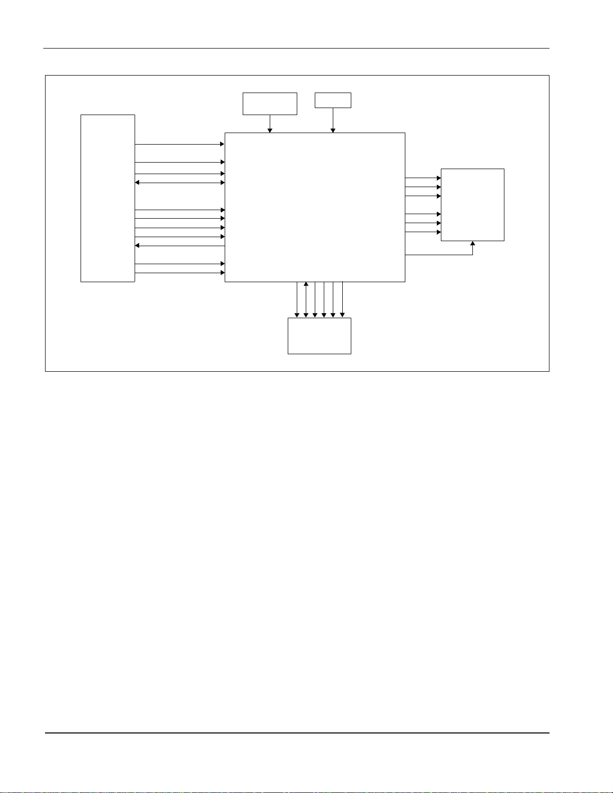
4 Block Description
4.1 Functional Block Diagram
16-bit FPM/EDO
DRAM
Register
CPU
R/W
Host
CPU / MPU
I/F
Bus Clock Memory Clock Pixel Clock
Figure 4-1: System Block Diagram Showing Datapaths
4.2 Functional Block Descriptions
Memory
Controller
Display
FIFO
Power Save
Clocks
Look-Up
Table
CRTC
LCD
I/F
LCD
DAC
Data
DAC
Control
4.2.1 Host Interface
The Host Interface block provides the means for the CPU/MPU to communicate with the display
buffer and internal registers, via one of the supported bus interfaces.
4.2.2 Memory Controller
The Memory Controller block arbitrates between CPU accesses and display refresh accesses as well
as generates the necessary signals to interface to one of th e supported 16-bit memory d evices (FPMDRAM or EDO-DRAM).
4.2.3 Display FIFO
The Display FIFO block fetches display data from the Memory Controller for display refresh.
Hardware Functional Specification S1D13504
Issue Date: 01/01/30 X19A-A-002-18
Page 24

Page 18 Epson Research and Development
Vancouver Design Center
4.2.4 Look-Up Table
The Look-Up Table block contains three 16x4 Look-Up Tables, one for each primary color. In
monochrome mode only one of these Look-Up Tables is selected and used.
4.2.5 LCD Interface
The LCD Interface block performs frame rate modulation for passiv e LCD panels. It also g enerates
the correct data format and timing control signals for various LCD and TFT panels.
4.2.6 Power Save
The Power Save block contains the power save mode circuitry.
S1D13504 Hardware Functional Specification
X19A-A-002-18 Issue Date: 01/01/30
Page 25
Epson Research and Development Page 19
Vancouver Design Center
5 Pin Out
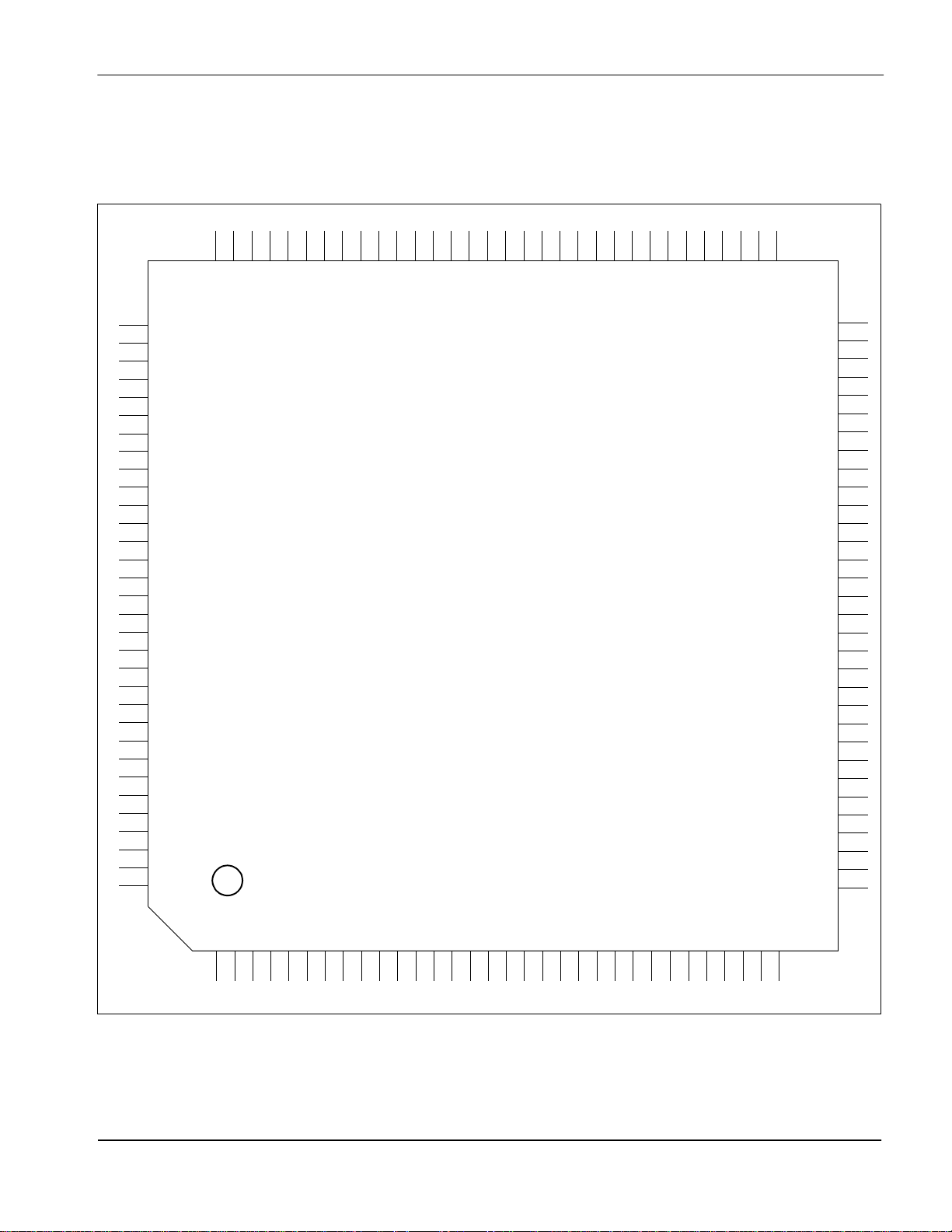
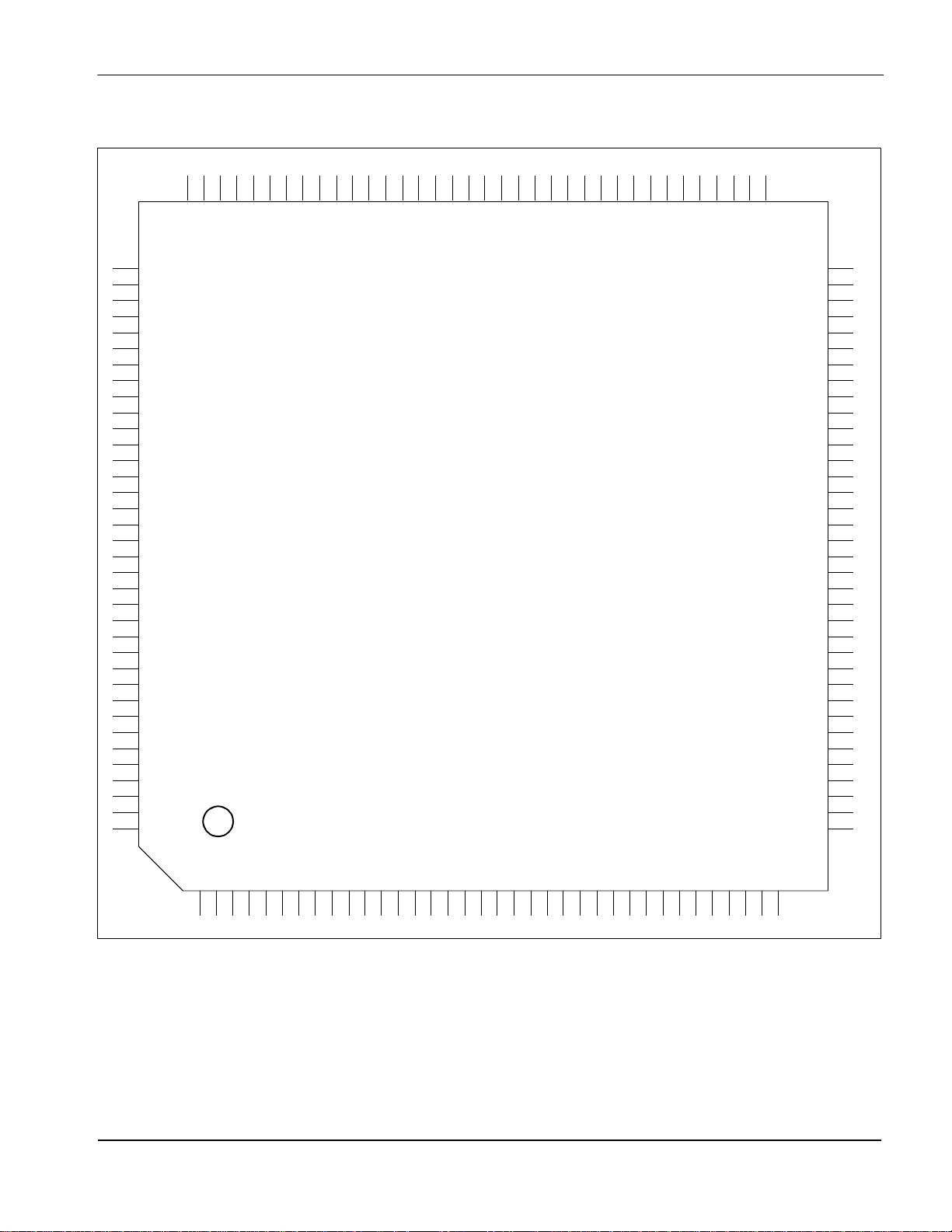
5.1 Pinout Diagram for S1D13504F00A
97
98
99
100
101
102
103
104
105
106
107
108
109
110
111
112
113
114
115
116
117
118
119
120
121
122
123
124
125
126
127
128
COREVDD
DACP0
DACWR#
DACRS0
DACRS1
HRTC
VRTC
VSS
CLKI
SUSPEND#
TESTEN
BUSCLK
VSS
IOVDD
AB20
AB19
AB18
AB17
AB16
AB15
AB14
AB13
AB12
AB11
AB10
AB9
AB8
AB7
AB6
AB5
AB4
AB3
96 95 94 93 92 91 90 89 88 87 86 85 84 83 7475 73 72 71 70 69 68 67 66 6582 81 80 79 78 77 76
VSS
FPDAT13
FPDAT15
FPDAT14
FPDAT10
FPDAT12
FPDAT9
FPDAT11
FPDAT8
VSS
DACCLK
BLANK#
DACRD#
IOVDD
FPDAT7
FPDAT6
FPDAT5
FPDAT4
FPDAT3
FPDAT2
S1D13504F00A
RD/WR#
RESET#
WAIT#
IOVDD
AB2
AB1
BS#
RD#
WE0#
M/R#
CS#
AB0
WE1#
GPIO0
VSS
DB15
DB14
DB12
DB13
DB11
FPDAT1
DB10
FPDAT0
DB9
VSS
DB8
FPSHIFT
DB7
DRDY
DB6
LCDPWR
DB5
FPLINE
DB4
FPFRAME
DB3
VSS
DB2
MD15
DB1
MD0
DB0
MD14
VSS
MD1
MD13
MD2
MD12
MD3
MD11
MD4
MD10
MD5
MD9
MD6
MD8
MD7
VSS
LCAS#
UCAS#
WE#
RAS#
IOVDD
MA9
MA11
MA8
MA10
MA7
MA0
MA6
MA1
MA5
MA2
MA4
MA3
COREVDD
64
63
62
61
60
59
58
57
56
55
54
53
52
51
50
49
48
47
46
45
44
43
42
41
40
39
38
37
36
35
34
33
1234567891011121314151617181920212223242526272829303132
Figure 5-1: Pinout Diagr am of F 00 A
Package type: 128 pin surface mount QFP15
Hardware Functional Specification S1D13504
Issue Date: 01/01/30 X19A-A-002-18
Page 26
Page 20 Epson Research and Development
Vancouver Design Center
5.2 Pinout Diagram for S1D13504F01A
97
98
99
100
101
102
103
104
105
106
107
108
109
110
111
112
113
114
115
116
117
118
119
120
121
122
123
124
125
126
127
128
COREVDD
DACP0
DACWR#
DACRS0
DACRS1
HRTC
VRTC
VSS
CLKI
SUSPEND#
TESTEN
BUSCLK
VSS
IOVDD
AB20
AB19
AB18
AB17
AB16
AB15
AB14
AB13
AB12
AB11
AB10
AB9
AB8
AB7
AB6
AB5
AB4
AB3
96 95 94 93 92 91 90 89 88 87 86 85 84 83 7475 73 72 71 70 69 68 67 66 6582 81 80 79 78 77 76
VSS
FPDAT13
FPDAT15
FPDAT14
FPDAT10
FPDAT12
FPDAT9
FPDAT11
FPDAT8
VSS
DACCLK
BLANK#
DACRD#
IOVDD
FPDAT7
FPDAT6
FPDAT5
FPDAT4
FPDAT3
FPDAT2
S1D13504F01A
RD/WR#
RESET#
WAIT#
IOVDD
AB2
AB1
BS#
RD#
WE0#
M/R#
CS#
AB0
WE1#
GPIO0
VSS
DB15
DB14
DB12
DB13
DB11
FPDAT1
DB10
FPDAT0
DB9
VSS
DB8
FPSHIFT
DB7
DRDY
DB6
LCDPWR
DB5
FPLINE
DB4
FPFRAME
DB3
VSS
DB2
MD15
DB1
MD0
DB0
MD14
VSS
MD1
MD13
MD2
MD12
MD3
MD11
MD4
MD10
MD5
MD9
MD6
MD8
MD7
VSS
LCAS#
UCAS#
WE#
RAS#
IOVDD
MA9
MA11
MA8
MA10
MA7
MA0
MA6
MA1
MA5
MA2
MA4
MA3
COREVDD
64
63
62
61
60
59
58
57
56
55
54
53
52
51
50
49
48
47
46
45
44
43
42
41
40
39
38
37
36
35
34
33
1234567891011121314151617181920212223242526272829303132
Figure 5-2: Pinout Diagram of F01A
Package type: 128 pin surface mount TQFP15
S1D13504 Hardware Functional Specification
X19A-A-002-18 Issue Date: 01/01/30
Page 27
Epson Research and Development Page 21
Vancouver Design Center
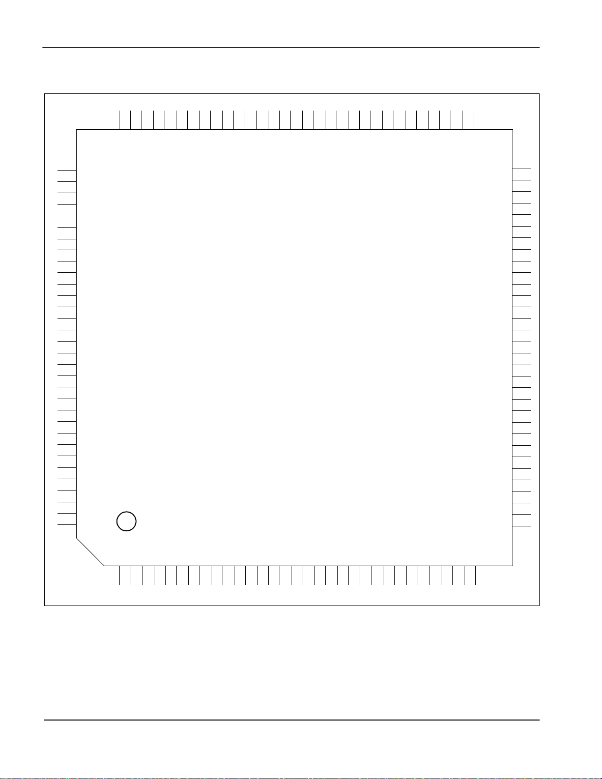
5.3 Pinout Diagram for S1D13504F02A
109
110
111
112
113
114
115
116
117
118
119
120
121
122
123
124
125
126
127
128
129
130
131
132
133
134
135
136
137
138
139
140
141
142
143
144
108107106105104103102101100
FPDAT15
VSS
NC
NC
NC
NC
COREVDD
DACP0
DACWR#
DACRS0
DACRS1
HRTC
VRTC
VSS
CLKI
SUSPEND#
TESTEN
BUSCLK
VSS
IOVDD
AB20
AB19
AB18
AB17
AB16
AB15
AB14
AB13
AB12
AB11
AB10
AB9
AB8
AB7
AB6
AB5
AB4
AB3
NC
NC
AB2
NC
NC
9998 97 96 95 94 93 92 91 90 89 88 878685 84 8382 81 80 79 78 77 76 75 7473
FPDAT13
FPDAT14
FPDAT10
FPDAT12
FPDAT9
FPDAT11
DACCLK
VSS
FPDAT8
IOVDD
FPDAT7
DACRD#
BLANK#
FPDAT6
S1D13504F02A
RD/WR#
M/R#
CS#
AB0
AB1
WE0#
RD#
BS#
RESET#
WE1#
IOVDD
WAIT#
GPIO0
VSS
FPDAT3
FPDAT2
FPDAT4
FPDAT5
DB15
DB14
DB12
DB13
VSS
FPSHIFT
DRDY
LCDPWR
FPLINE
FPFRAME
VSS
MD15
MD14
FPDAT0
FPDAT1
DB10
DB11
DB8
DB9
DB5
DB7
DB4
DB6
MD0
NC
NC
72
NC
71
NC
MD1
70
MD13
69
68
MD2
67
MD12
66
MD3
65
MD11
64
MD4
63
MD10
62
MD5
61
MD9
60
MD6
59
MD8
58
MD7
57
VSS
56
LCAS#
55
UCAS#
54
WE#
53
RAS#
52
IOVDD
51
MA9
50
MA11
49
MA8
48
MA10
47
MA7
46
MA0
45
MA6
44
MA1
43
MA5
42
MA2
41
MA4
40
MA3
NC
NC
39
38
37
COREVDD
DB3
DB2
VSS
DB1
DB0
NC
NC
1 2 3 4 5 6 7 8 9 101112 131415 16 171819 20 21 22 23 24 25 2627 28 293031 32 33 34 35 36
Figure 5-3: Pinout Diagr am of F 02 A
Package type: 144 pin surface mount QFP20
Hardware Functional Specification S1D13504
Issue Date: 01/01/30 X19A-A-002-18
Page 28
Page 22 Epson Research and Development
Vancouver Design Center
5.4 Pin Description
Key:
I = Input
O = Output
IO = Bi-Directional (Input/Output)
P=Power pin
C = CMOS level input
CD = CMOS level input with pull-down resistor (typical values of 100KΩ/180KΩ at 5V/3.3V respectively)
CS = CMOS level Schmitt input
COx = CMOS output driver, x denotes driver type (1=3/-1.5mA, 2=6/-3mA, 3=12/-6mA)
TSx = Tri-state CMOS output driver, x denotes driver type (1=3/-1.5mA, 2=6/-3mA, 3=12/-6mA)
TSxD =
CNx = CMOS lo w-noi se output driver, x denotes driver type (1=3/-1. 5m A, 2=6/-3 mA, 3=12/-6m A)
Tri-state CMOS output driver with pull-down resistor (typical values of 100KΩ/180KΩ at 5V/3.3V
respectively), x denotes driver type (1=3/-1.5mA, 2=6/-3mA, 3=12/-6mA)
5.4.1 Host Interface
Table 5-1: Host Interface Pin Descriptions
Pin #
Pin Name Type
AB0 I 3 5 CS Hi-Z
AB[20:1] I
DB[15:0] IO 16-31 18-33 C/TS2 Hi-Z
F00A
F01A
111-128
1, 2
F02A
125-142
3,4
Driver
C Hi-Z System address bus bits [20:1].
Reset =
0 Value
Description
This pin has multiple functions.
• F or SH-3 m ode, this pin inputs system address bit 0 (A0).
• For MC68K Bus 1, this pin inputs the lower data strobe (LDS#).
• For MC68K Bus 2, this pin inputs system address bit 0 (A0).
• For Generic Bus, this pin inputs system address bit 0 (A0).
See Table 5-9: “Host Bus Interface Pin Mapping,” on page 32 for
summary.
System data bus. Unused data pins should be connected to IO
V
.
DD
• For SH-3 mode, these pins are connected to D[15:0].
• For MC68K Bus 1, these pins are connected to D[15:0].
• F or MC68K Bus 2, these pins are c onnected to D[31:16] for 32bit devices (e.g. MC68030) or D[15:0] for 16-bit devices (e.g.
MC68340).
• F or Gen eric Bu s , these pi n s are connected to D[15:0].
See Table 5-9: “Host Bus Interface Pin Mapping,” on page 32
summary.
for
S1D13504 Hardware Functional Specification
X19A-A-002-18 Issue Date: 01/01/30
Page 29
Epson Research and Development Page 23
Vancouver Design Center
Table 5-1: Host Inter face Pin Descriptions (Continued )
Pin Name Type
F00A
F01A
Pin #
F02A
Driver
Reset =
0 Value
Description
This pin has multiple functions.
• For SH-3 mode, this pin inputs the write enable signal for the
upper data byte (WE1#).
• For MC68K Bus 1, this pin inputs the upper data strobe
WE1# I 9 11 CS Hi-Z
(UDS#).
• For MC68K Bus 2, this pin inputs the data strobe (DS#).
• For Generic Bus, this pin inputs the write enable signal for the
upper data byte (WE1#).
See Table 5-9: “Host Bus Interfa ce Pin Ma ppi ng,” on page 32.
This input pin is used to select between the memory and register
address spaces of the S1D13504. M/R# is set high to access the
M/R# I 5 7 C Hi-Z
memory and low to access the registers. See Section 8.1,
“Register Mapping”
on page 90
.
See Table 5-9: “Host Bus Interfa ce Pin Ma ppi ng,” on page 32.
CS# I 4 6 C Hi-Z
BUSCLK I 108 122 C Hi-Z
Chip select input. See Table 5-9: “Host Bus Interface Pin
Mapping,” on page 32.
System bus clock. See Table 5-9: “Host Bus Interface Pin
Mapping,” on page 32.
This pin has multiple functions.
• For SH-3 mode, this pin inputs the bus start signal (BS#).
BS# I 6 8 CS Hi-Z
• For MC68K Bus 1, this pin inputs the address strobe (AS#).
• For MC68K Bus 2, this pin inputs the address strobe (AS#).
• For Generic Bus, this pin must be tied to IO V
DD
.
See Table 5-9: “Host Bus Interfa ce Pin Ma ppi ng,” on page 32.
This pin has multiple functions.
• For SH-3 mode, this pin inputs the RD/WR# signal. The
S1D13504 needs this si gnal for early decode of the bus cycle.
RD/WR# I 10 12 CS Hi-Z
• For MC68K Bus 1, this pin inputs the R/W# signal.
• For MC68K Bus 2, this pin inputs the R/W# signal.
• For Generic Bus, this pin inputs the read command for the
upper data byte (RD1# ).
See Table 5-9: “Host Bus Interfa ce Pin Ma ppi ng,” on page 32.
This pin has multiple functions.
• For SH-3 mode, this pin inputs the read signal (RD#).
• For MC68K Bus 1, this pin must be tied to IO V
RD#I79CSHi-Z
• For MC68K Bus 2, this pin inputs the bus size bit 1 (SIZ1).
DD
.
• For Generic Bus, this pin inputs the read command for the
lower data byte (RD0#).
See Table 5-9: “Host Bus Interfa ce Pin Ma ppi ng,” on page 32.
Hardware Functional Specification S1D13504
Issue Date: 01/01/30 X19A-A-002-18
Page 30
Page 24 Epson Research and Development
Vancouver Design Center
Table 5-1: Host Interface Pin Descriptions (Continued)
Pin Name Type
F00A
F01A
Pin #
F02A
Driver
Reset =
0 Value
Description
This pin has multiple functions.
• For SH-3 mode, this pin inputs the write enable signal for the
lower data byte (WE0#).
WE0# I 8 10 CS Hi-Z
• For MC68K Bus 1, this pin must be tied to IO V
• For MC68K Bus 2, this pin inputs the bus size bit 0 (SIZ0).
DD.
• For Generic Bus, this pin inputs the write enable signal for the
lower data byte (WE0#).
See Table 5-9: “Host Bus Interface Pin Mapping,” on page 32.
The active polarity of the WAIT# out put is configurable on the
rising edge of RESET# - see Section 5.5,
Configuration Opti ons”
on page 31.
“Summary of
This pin has multiple functions.
• F or SH-3 m ode, this pin outputs the wait reques t sign al
(WAIT#); MD5 must be pulled low during reset by the internal
pull-down resistor.
WAIT# O 13 15 TS2 Hi-Z
• For MC68K Bus 1, this pin outputs the data transfer
acknowle dge signal (DTACK#); MD5 m u st be pull ed high
during reset by an external pull-up resistor.
• For MC68K Bus 2, this pin outputs the data transfer and size
acknowle dge bit 1 (DSACK1#); MD5 must be pulled high
during reset by an external pull-up resistor.
• F or Generic Bus , thi s pin ou tputs th e wai t signa l (WAIT#); MD5
must be pulled low du ring res et by the internal pull-down
resistor.
See Table 5-9: “Host Bus Interface Pin Mapping,” on page 32.
RESET# I 11 13 CS Input 0
Active low input to clear all internal registers and to force all
signals to their inacti ve states.
S1D13504 Hardware Functional Specification
X19A-A-002-18 Issue Date: 01/01/30
Page 31

Epson Research and Development Page 25
Vancouver Design Center
5.4.2 Memory Interface
Table 5-2: Memory Interface Pin Descriptions
Pin #
Pin Name Type
F00A
F01A
F02A
Driver
LCAS#O5056CO1Output 1
UCAS#O4955CO1Output 1
Reset = 0
Value
Description
This pin has multiple functions.
• F or dual C AS# DRAM , th is is th e colu mn address strobe for
the lower byte (LCAS#).
• F or sin gle CAS# DRAM, this is the column address stro be
(CAS#).
See Table 5-10: “Memory Interface Pin Mapping,” on page 32
for summary.
This pin has multiple functions.
• F or dual C AS# DRAM , th is is th e colu mn address strobe for
the upper byte (UCAS#).
• F or single CAS# DRAM, this is the write e nabl e signal f or th e
upper byte (UWE#).
See Table 5-10: “Memory Interface Pin Mapping,” on page 32
for summary.
This pin has multiple functions.
• F or dual CAS# DRAM, this is the write enable signa l (W E#).
WE# O 48 54 CO1 Output 1
• F or single CAS# DRAM, this is the write e nabl e signal f or th e
lower byte (LWE#).
See Table 5-10: “Memory Interface Pin Mapping,” on page 32
for summary.
RAS# O 47 53 CO1 Output 1 Row address strobe.
These pins have mu ltip le functions.
• Bi-directional memory data bus.
• During reset, these pins are inputs and their states at the
rising edge of RESET# are used to configure the chip.
Internal pull-down resist ors (typ ic al values of
100KΩ/100KΩ/120KΩ at 5.0V/3.3V/3.0V respectively) pull
the reset states to 0. External pull-up resistors can be used
to pull the reset states to 1. See Section 5.5,
Configuration Op tio n s”
MD[15:0] IO
67, 65,
63, 61,
59, 57,
55, 53,
52, 54,
56, 58,
60, 62,
64, 66
76, 70,
68, 66,
64, 62,
60, 58,
59, 61,
63, 65,
67, 69,
75, 77
CD2/TS1
Hi-Z
(pulled 0)
“Summary of
on page 31.
Hardware Functional Specification S1D13504
Issue Date: 01/01/30 X19A-A-002-18
Page 32

Page 26 Epson Research and Development
Vancouver Design Center
Table 5-2: Memory Int er face Pin Descriptions (Continued )
Pin #
Pin Name Type
MA[8:0] O
F00A
F01A
43, 41,
39, 37,
35, 34,
36, 38,
40
F02A
46, 44,
42, 40,
41, 43,
45, 47,
49
Driver
CO1 Output 0 Multiplexed memory add res s.
MA9IO4551C/TS1
MA10 IO 42 48 C/TS1
Reset = 0
Hi-Z /
Output 0
Hi-Z /
Output 0
Value
Description
This pin has multiple functions.
• F or 2M byte DRAM, this is memory address bit 9 (MA9).
• F or asymmetrical 512K byte DRAM, th is is memory address
bit 9 (MA9).
1
• For symmetrical 512K byte DRAM, this pin can be used as
general purpose IO (GPIO3).
See Table 5-10: “Memory Interface Pin Mapping,” on page 32
for summary.
This pin has multiple functions.
• For asymmetrical 2M byte DRAM, this is memory address bit
10 (MA10).
• For symmetrical 2M byte DRAM and all 512K byte DRAM,
1
this pin can be used as gener al purpose IO (GPIO1).
See Table 5-10: “Memory Interface Pin Mapping,” on page 32
for summary.
MA11 IO 44 50 C/TS1
1 When configured as IO pins.
Hi-Z /
Output 0
This pin has multiple functions.
• For asymmetrical 2M byte DRAM, this is memory address bit
11 (MA11).
• For symmetrical 2M byte DRAM and all 512K byte DRAM,
1
this pin can be used as gener al purpose IO (GPIO2).
See Table 5-10: “Memory Interface Pin Mapping,” on page 32
for summary.
S1D13504 Hardware Functional Specification
X19A-A-002-18 Issue Date: 01/01/30
Page 33

Epson Research and Development Page 27
Vancouver Design Center
5.4.3 LCD Interface
Table 5-3: LCD
Pin #
Pin Name Type
FPDAT[8:0] O 88, 82-75 98, 92-85 CN3 Output 0 Panel Data
FPDAT[15:9] O 95-89 105-99 CN3 Output 0
FPFRAME O 69 79 CN3 Output 0 Frame Pulse
FPLINE O 70 80 CN3 Output 0 Line Pulse
FPSHIFT O 73 83 CN3 Output 0 Shift Clock Pulse
LCDPWRO 7181CO1Output
F00A
F!A
F02A
Driver
Interface Pin Descriptions
Reset =
0 Value
These pins have mu ltiple functions.
• P a nel Data for 16-bit panels.
• Pixel Data for external RAMDA C sup po rt.
See Table 5-11: “LCD, CRT, RAMDAC I nterface Pin
Mapping,” on page 33.
LCD power control output. Th e active polarit y of this output
is selected by the state of MD10 at the risi ng edg e of
RESET# - see Section 5.5,
1
Options”
This output is controlle d by the power sa ve mode ci rcuitry see Section 13,
details.
on page 31.
Description
“Summary of Configurati on
“Power Save Modes”
on page 128 for
DRDY O 72 82 CN3 Output 0
1 Output may be 1 or 0.
5.4.4 Clock Input
Table 5-4: Clock Input
Pin #
Pin Name T ype
CLKI I 105 119 C Hi-Z
F00A
F01A
F02A
Driver
Reset =
0 Value
This pin has multiple functions which are automatically
selected depending on panel type used.
• F or T FT panels, this is the display enable output
(DRDY).
• F or pas si ve LCDs with Format 1 interfaces, this is the
2nd Shift Clock (FPSHIFT2).
• F or all other LCD p anels , th is is the L CD ba c kplane b ias
signal (MOD).
See Table 5-11: “LCD, CRT, RAMDAC I nterface Pin
Mapping,” on page 33
and REG[02h] for details.
Pin Description
Description
Input clock for the internal pixel cl ock (PCL K) an d memory
clock (MCLK). PCLK and MCLK are derived fr om CLKI – see
REG[19h] for details.
Hardware Functional Specification S1D13504
Issue Date: 01/01/30 X19A-A-002-18
Page 34

Page 28 Epson Research and Development
Vancouver Design Center
5.4.5 CRT and External RAMDAC Interface
Table 5-5: CRT an d RAM D A C
Pin #
Pin Name Type
F00A
F01A
F02A
Driver
DACRD# IO 84 94 C/TS1
DACWR# IO 99 113 C/TS1
DACRS1 IO 101 115 C/TS1
DACRS0 IO 100 114 C/TS1
Interface Pin Descriptions
Reset = 0
Value
This pin has multiple functions.
Hi-Z /
Output 1
Hi-Z /
Output 1
Hi-Z /
Output 0
Hi-Z /
Output 0
• Read signal for external RAMDAC support.
• General Purpose IO (G PIO 4).
1
See Table 5-11: “LCD, CRT, RAMDAC Interface Pin
Mapping,” on page 33.
This pin has multiple functions.
• Write signal for external RAMDAC support.
• General Purpose IO (G PIO 7).
1
See Table 5-11: “LCD, CRT, RAMDAC Interface Pin
Mapping,” on page 33.
This pin has multiple functions.
• Register Select bit 1 for external RAMDAC support.
• General Purpose IO (G PIO 9).
1
See Table 5-11: “LCD, CRT, RAMDAC Interface Pin
Mapping,” on page 33.
This pin has multiple functions.
• Register Select bit 0 for external RAMDAC support.
• General Purpose IO (G PIO 8).
1
See Table 5-11: “LCD, CRT, RAMDAC Interface Pin
Mapping,” on page 33.
Description
DACP0 IO 98 112 C/CN3
Hi-Z /
Output 0
This pin has multiple functions.
• Pixel Data bit 0 for external RAMDAC support.
• General Purpose IO (G PIO 6).
1
See Table 5-11: “LCD, CRT, RAMDAC Interface Pin
Mapping,” on page 33.
S1D13504 Hardware Functional Specification
X19A-A-002-18 Issue Date: 01/01/30
Page 35

Epson Research and Development Page 29
Vancouver Design Center
Pin Name Type
Table 5-5: CRT and RAMDAC
Pin #
F00A
F01A
F02A
Driver
Interface Pin Descriptions (Continued)
Reset = 0
Value
Description
This pin has multi ple functions.
• Horizon tal Retrace signal for CR T.
• General Purpose IO (GPIO10).
1
HRTC IO 102 116 C/CN3
Hi-Z /
Output 0
See Table 5-11: “LCD, CRT, RAMDAC Inte rfac e Pin
Mapping,” on page 33.
This pin has multi ple functions.
• Vertical Retrace signal for CRT.
• General Purpose IO (GPIO11).
1
VRTC IO 103 117 C/CN3
Hi-Z /
Output 0
See Table 5-11: “LCD, CRT, RAMDAC Inte rfac e Pin
Mapping,” on page 33.
This pin has multi ple functions.
• Blanki ng si gna l for DAC .
• General Purpose IO (GPIO5).
1
BLANK# IO 85 95 C/CN3
Hi-Z /
Output 0
See Table 5-11: “LCD, CRT, RAMDAC Inte rfac e Pin
Mapping,” on page 33.
DACCLK O 86 96 C/CN3 Output 0 Pixel Clock for RAMDAC.
1 When configured as IO pins
Hardware Functional Specification S1D13504
Issue Date: 01/01/30 X19A-A-002-18
Page 36

Page 30 Epson Research and Development
Vancouver Design Center
5.4.6 Miscellaneous
Pin Name Type
F00A
F01A
Pin #
Table 5-6: Miscellaneous
F02A
Driver
Reset = 0
Pin Descriptions
Value
Description
This pin has multiple functions.
• When MD 9 = 0 at rising ed ge of RESET#, this pi n is
an active-low input used to place the S1D13504 into
suspend mode; see Section 13,
on page 128 for details.
• When MD[10:9] = 01 at rising edge of RESET#, this
pin is an output with a reset state of 0. Its state is
SUSPEND# IO 106 120 CS/TS1
Hi-Z /
Output
1
controlled b y REG[2 1h] bi t 7.
• When MD[10:9] = 11 at rising edge of RESET#, this
pin is an output with a reset state of 1. Its state is
controlled b y REG[2 1h] bi t 7.
GPIO0 IO 12 14 C/TS1 Hi-Z General Purpose IO pin 0.
TSTEN I 107 121 CD
Hi-Z
(pulled 0)
Test Enable. This in shoul d be connected to VSS for
normal operation.
1, 2, 3538, 71-
NC - -
74, 107-
- - No connect
110, 143,
144
“Power Save Modes”
1 When configured as IO pin. Output may be 1 or 0.
5.4.7 Power Supply
Table 5-7: Power Supply
Pin #
Pin Name Type
F00A
F01A
F02A
COREVDD P 33, 97 39, 111 P Core V
IOVDD P
VSS P
14, 46, 83,
110
15, 32, 51,
68, 74, 87,
96, 104,
109
16, 52, 93,
124
17, 34, 57,
78, 84, 97,
106, 118,
123,
Pin Descriptions
Driver Description
PIO V
P Common V
DD
DD
SS
S1D13504 Hardware Functional Specification
X19A-A-002-18 Issue Date: 01/01/30
Page 37

Epson Research and Development Page 31
Vancouver Design Center
5.5 Summary of Configuration Options
Table 5-8: Summary of Power On / Reset Options
Pin Name
MD0 8-bit host bus interface 16-bit host bus interfa ce
Select host bus interface:
000 = SH-3 bus interface
MD[3:1]
001 = MC68K bus 1 (e.g. MC68000)
010 = MC68K bus 2 (e.g. MC68030)
011 = Generic bus interface (e.g. Philips MIPS PR31500/PR31700; NEC MIPS V
1XX = reserved
MD4 Little Endian Big Endian
MD5 WAIT# is active high (1 = insert wait state ) WAIT# is active low (0 = insert wait state)
Memory Address/GPIO configuration:
00 = symmetrical 256K×16 DRAM. MA[8:0] = DRAM address. MA[11:9] = GPIO[2:1] and GPIO3.
MD[7:6]
01 = symmetrical 1M×16 DRAM . MA[9:0] = DRAM address. MA[11:10] = GPIO[2:1].
10 = asymmetrical 256K×16 DRAM. MA[9:0] = DRAM address. MA[11:10] = GPIO[2:1].
11 = asymmetrical 1M×16 DRAM. MA[11:0] = DRAM address.
Configure DACRD#, BLANK#, DACP0, DACWR#,
MD8
DACRS0, DACRS1, HRTC, VRTC as General
Purpose IO (GPIO[11:4]).
MD9 SUSPEND# pin configured as GPO output. SUSPEND# pin configured as SUSPEND# input.
value on this pin at rising edge of RESET# is used to configure : (1/0)
10
4102)
R
Configure DACRD#, BLANK#, DACP0, DACWR#,
DACRS0, DACRS1, HRTC, VRTC as DAC and CRT
outputs.
MD10 Active low LCDPWR or GPO polarities. Act iv e high LCDPWR or GPO polarities .
MD[15:11] Not used.
Hardware Functional Specification S1D13504
Issue Date: 01/01/30 X19A-A-002-18
Page 38

Page 32 Epson Research and Development
Vancouver Design Center
5.6 Multiple Function Pin Mapping
Table 5-9: Host Bus Interface Pin Mapping
S1D13504
Pin Names
AB[20:1] A[20:1] A[20:1] A[20:1] A[20:1]
AB0 A0 LDS# A0 A0
DB[15:0] D[15:0] D[15:0] D[31:16] D[15:0]
WE1# WE1# UDS# DS# WE1#
M/R# External Decode External Deco de External Decode External Decode
CS# CSn# External Decode External Decode External Decode
BUSCLK CKIO CLK CLK BCLK
BS# BS# AS# AS# Connect to IO V
RD/WR# RD/WR# R/W# R/W# RD1#
RD# RD# Connect to IO V
WE0# WE0# Connect to IO V
WAIT# WAIT# DTACK# DSACK1# WAIT#
RESET# RESET# RESET# RESET# RESET#
SH-3 MC68K Bus 1 MC68K Bus 2 Generic MPU
DD
DD
SIZ1 RD0#
SIZ0 WE0#
DD
Table 5-10: Memory Interface Pin Mapping
S1D13504
Pin Names
Sym 256Kx16 Asym 256Kx16 Sym 1Mx16 Asym 1Mx16
FPM/EDO-DRAM
2-CAS# 2-WE# 2-CAS# 2-WE# 2-CAS# 2-WE# 2-CAS# 2-WE#
MD[15:0] DQ[15:0]
MA[8:0] A[8:0]
MA9 GPIO3
1
MA10 GPIO1
MA11 GPIO2
1
1
A9
A10
A11
UCAS# UCAS# UWE# UCAS# UWE# UCAS# UWE# UCAS# UWE#
LCAS# LCAS# CAS# LCAS# CAS# LCAS# CAS# LCAS# CAS#
WE# WE# LWE# WE# LWE# WE# LWE# WE# LWE#
RAS# RAS#
Note
1. All GPIO pins default to input on reset, and unless programmed otherwise should be
connected to either V
or IO VDD if not used.
SS
S1D13504 Hardware Functional Specification
X19A-A-002-18 Issue Date: 01/01/30
Page 39

Epson Research and Development Page 33
Vancouver Design Center
Table 5-11: LCD, CRT, RAMDAC Interface P in Mapping
Monochrome Passive
S1D13504
Pin Names
Panel
Single Dual Single
4-bit 8-bit 8-bit 4-bit 8-bit 8-bit 8-bit 16-bit 9-bit 12-bit 18-bit
FPFRAME FPFRAME Note
FPLINE FPLINE Note
FPSHIFT FPSHIFT Note
DRDY MOD FPSHIFT2 MOD DRDY Note
FPDAT0 driven 0 D0 LD0 driven 0 D0 D0 LD0 LD0 R2 R3 R5 Note
FPDAT1 driven 0 D1 LD1 driven 0 D1 D1 LD1 LD1 R1 R2 R4 Note
FPDAT2 driven 0 D2 LD2 driven 0 D2 D2 LD2 LD2 R0 R1 R3 Note
FPDAT3 driven 0 D3 LD3 driven 0 D3 D3 LD3 LD3 G2 G3 G5 Note
FPDAT4 D0 D4 UD 0 D0 D4 D4 UD 0 UD0 G1 G2 G4 Note
FPDAT5 D1 D5 UD 1 D1 D5 D5 UD 1 UD1 G0 G1 G3 Note
FPDAT6 D2 D6 UD2 D2 D6 D6 UD2 UD2 B2 B3 B5 Note
FPDAT7 D3 D7 UD3 D3 D7 D7 UD3 UD3 B1 B2 B4 Note
FPDAT8 driven 0 driven 0 driven 0 driven 0 driven 0 driven 0 driven 0 LD4 B0 B1 B3 Note
Color Passive Panel
Single
Format 1
Single
Format 2
Dual
Color TFT Panel
CRT
1
2
2
2
2
2
2
2
2
2
2
2
2
2
FPDAT9 driven 0 driven 0 driven 0 driven 0 driven 0 driven 0 driven 0 LD5 driven 0 R0 R2 DACP7
FPDAT10 driven 0 driven 0 driven 0 driven 0 driven 0 driven 0 driven 0 LD6 driven 0 driven 0 R1 DACP6
FPDAT11
driven 0 driven 0 driven 0 driven 0 driven 0 driven 0 driven 0 LD7 driven 0 G0 G2 DACP5
FPDAT12 driven 0 driven 0 driven 0 driven 0 driven 0 driven 0 driven 0 UD4 driven 0 driven 0 G1 DACP4
FPDAT13
driven 0 driven 0 driven 0 driven 0 driven 0 driven 0 driven 0 UD5 driven 0 driven 0 G0 DACP3
FPDAT14 driven 0 driven 0 driven 0 driven 0 driven 0 driven 0 driven 0 UD6 driven 0 B0 B2 DACP2
FPDAT15
DACRD# GPIO4
BLANK# GPIO5
DACP0 GPIO6
DACWR# GPIO7
DACRS0 GPIO8
DACRS1 GPIO9
HRTC GPIO10
VRTC GPIO11
driven 0 driven 0 driven 0 driven 0 driven 0 driven 0 driven 0 UD7 driven 0 driven 0 B1 DACP1
3
3
3
3
3
3
3
3
DACRD#
BLANK#
DACP0
DACWR#
DACRS0
DACRS1
HRTC
VRTC
DACCLK driven 0 DACCLK
Note
1. Although 18-bit TFT panels are supported only 16 data bits (64K colors) are available
- R0 and B0 are not used.
2. If no LCD is active these pins are driven low.
3. All GPIO pins default to input on reset, and unless programmed otherwise should be
connected to either V
Hardware Functional Specification S1D13504
Issue Date: 01/01/30 X19A-A-002-18
or IO VDD if not used.
SS
Page 40

Page 34 Epson Research and Development
Vancouver Design Center
6 D.C. Characteristics
Table 6-1: Absolute Maximum Ratings
Symbol Parameter Rating Units
Core V
IO V
DD
V
IN
V
OUT
T
STG
T
SOL
DD
Supply Voltage VSS - 0.3 to 4.6 V
Supply Voltage VSS - 0.3 to 6.0 V
Input Voltage VSS - 0.3 to IO VDD + 0.5 V
Output Voltage VSS - 0.3 to IO VDD + 0.5 V
Storage Temperature -65 to 150 ° C
Solder Temperature/Time 260 for 10 sec. max at lead ° C
Table 6-2: Recommended Operating Conditions
Symbol Parameter Condition Min Typ Max Units
Core V
IO V
DD
V
IN
T
OPR
DD
Supply Voltage VSS = 0 V 2.7 3.0/3.3 3.6 V
Supply Voltage VSS = 0 V 2.7 3.0/3.3/5.0 5.5 V
Input Voltage V
SS
IO V
DD
Operating Temperature -40 25 85 ° C
Table 6-3: Input Specifications
Symbol Parameter Condition Min Typ Max Units
V
V
V
V
V
I
IZ
C
HR
IL
IH
T+
T-
Low Level Input Voltage
CMOS inputs
High Level Input Voltage
CMOS inputs
Positive-Going Threshold
CMOS Schmitt inputs
Negative-Going Threshold
CMOS Schmitt inputs
Input Leakage Current
IN
PD
Input Pin Capacitance 10 pF
Pull-down Resistance
IO VDD = 3.0
3.3
5.0
IO VDD = 3.0
3.3
5.0
IO VDD = 3.0
3.3
5.0
IO VDD = 3.0
3.3
5.0
V
= Max
DD
= IO V
V
IH
V
IL
V
IN
DD
= V
SS
= VDD= 3.0
= 3.3
= 5.0
1.9
2.0
3.5
1.0
1.1
2.0
0.5
0.6
0.8
0.8
0.8
1.0
2.3
2.4
4.0
1.7
1.8
3.1
V
V
V
V
V
V
V
V
V
V
V
V
-1 1 µA
60
50
50
120
100
100
300
300
300
kΩ
kΩ
kΩ
S1D13504 Hardware Functional Specification
X19A-A-002-18 Issue Date: 01/01/30
Page 41

Epson Research and Development Page 35
Vancouver Design Center
Table 6-4: Output Specifications
Symbol Parameter Condition Min Typ Max Units
Low Level Output Voltage
V
OL
Type 1 - TS1, CO1, TS1D
Type 2 - TS2, CO2
Type 3 - TS3, CO3
= 3mA
I
OL
= 6mA
I
OL
= 12mA
I
OL
0.4 V
High Level Output Voltage
V
I
C
C
OH
OZ
OUT
BID
Type 1 - TS1, CO1, TS1D
Type 2 - TS2, CO2
Type 3 - TS3, CO3
Output Leakage Current
Output Pin Capacitance 10 pF
Bidirectional Pin Capa citance 10 pF
= -1.5 mA
I
OL
= -3 mA
I
OL
I
= -6 mA
OL
IO V
DD
= V
V
OH
V
= V
OL
= Max
DD
SS
IO V
- 0.4 V
DD
-1 1 µA
Hardware Functional Specification S1D13504
Issue Date: 01/01/30 X19A-A-002-18
Page 42

Page 36 Epson Research and Development
Vancouver Design Center
7 A.C. Charac teristics
Conditions: IO VDD = 2.7V to 5.5V unless otherwise specified
T
= -40° C to 85° C
A
T
7.1 CPU Interface Timing
7.1.1 SH-3 Interface Timing
t1 t2 t3
CKIO
and T
rise
C
= 50pF (Bus / MPU Interface)
L
C
= 100pF (LCD Panel Interface)
L
C
= 10pF (Display Buffer Interface)
L
C
= 10pF (CRT / DAC Interface)
L
for all inputs must be ≤ 5 nsec (10% ~ 90%)
fall
A[20:0], M/R#
RD/WR#
BS#
CSn#
WEn#
RD#
WAIT#
D[15:0](write)
D[15:0](read)
t4
t6 t7
t8
t11
t13
t5
t12
t9
t12
t14
t15
t10
t16
Figure 7-1: SH-3 Interface Timing
Note
The SH-3 Wait State Control Register for the area in which the S1D13504 resides must be set to
a non-zero value.
S1D13504 Hardware Functional Specification
X19A-A-002-18 Issue Date: 01/01/30
Page 43

Epson Research and Development Page 37
Vancouver Design Center
Table 7-1: SH-3 Interface Timing
Symbol Parameter Min Max Units
t9
t10
t11
t12
t13
t14
t15
t16
t1
t2
t3
t4
t5
t6
t7
t8
Clock period
Clock pulse wid th high
Clock pulse wid th lo w
A[20:0], M/R#, RD/WR# setup to CKIO
A[20:0], M/R#, RD/WR# hold from CS#
BS# setup
BS# hold
CSn# setup
2
Falling edge RD# to D[15:0] driven
Rising edge CSn# to WAIT# tri-state
1
Falling edge CSn# to WAIT# driven
CKIO to WAIT# delay
D[15:0] setup to first CKIO after BS# (write cyc le)
D[15:0] hold (write cycle)
D[15:0] valid to WAIT# rising ed ge (read cycle)
Rising edge RD# to D[15:0] tri-state (read cycle)
25 ns
5ns
5ns
4ns
0ns
3ns
0ns
0ns
3ns
04ns
111ns
315ns
0ns
0ns
0ns
29ns
1. If the S1D13504 host interface is disabled, the timing for WAIT# driven is relative to the falling edge of CSn# or
the first positive edge of CKIO after A[20:0] and M/R# become valid,
whichever occurs later.
2. If the S1D13504 host interface is disabled, the timing for D[15:0] driven is relative to the falling edge of RD# or
the first positive edge of CKIO after A[20:0] and M/R# become valid,
whichever occurs later.
Hardware Functional Specification S1D13504
Issue Date: 01/01/30 X19A-A-002-18
Page 44

Page 38 Epson Research and Development
Vancouver Design Center
7.1.2 MC68K Bus 1 Interface Timing (e.g. MC68000)
t1 t2 t3
CLK
A[20:1]
M/R#
CS#
AS#
UDS#
LDS#
R/W#
DTACK#
D[15:0](write)
t4
t5
t6
t16
t7
t9
t11
t12
t8
t10
t13
t14
t15
D[15:0](read)
Figure 7-2: MC68K Bus 1 Interface Timi ng
S1D13504 Hardware Functional Specification
X19A-A-002-18 Issue Date: 01/01/30
Page 45

Epson Research and Development Page 39
Vancouver Design Center
Table 7-2: MC68K Bus 1 Interface Timing
Symbol Parameter Min Max Units
t9
t10
t11
t12
t13
t14
t15
t16
t1
t2
t3
t4
t5
t6
t7
t8
1
Clock period
Clock pulse width high
Clock pulse width low
A[20:1], M/R# setup to first CLK where CS# = 0 AS# = 0, and
either UDS#=0 or LDS# = 0
A[20:1], M/R# hold from AS#
CS# hold from AS#
R/W# setup to before to either UDS#=0 or LDS# = 0
R/W# hold from AS#
AS# = 0 and CS# = 0 to DTACK# driven high
AS# high to DTACK# high impedance
D[15:0] valid to se co nd C L K wher e CS # = 0 AS # = 0, and either
UDS#=0 or LDS# = 0 (write cycle)
D[15:0] hold from falling edge of DTACK# (write cycle)
Falling edge of UDS#=0 or LDS# = 0 to D[15:0] driven (read
2
cycle)
D[15:0] valid to DTACK# falling edge (read cycle)
UDS# and LDS# high to D[15:0] invalid/high impedance (read
cycle)
AS# high setup to CLK
30 ns
5ns
5ns
4ns
0ns
0ns
5ns
0ns
1ns
15ns
0ns
0ns
3ns
0ns
211ns
3ns
1. If the S1D13504 host interface is disabled, the timing for DTACK# driven high is relative to
the falling edge of AS# or
the first positive edge of CLK after A[20:1] and M/R# become valid,
whichever occurs later.
2. If the S1D13504 host interface is disabled, the timing for D[15:0] driven is relative to the falling edge of UDS#/LDS# or
the first positive edge of CLK after A[20:1] and M/R# become val-
id, whichever occurs later.
Hardware Functional Specification S1D13504
Issue Date: 01/01/30 X19A-A-002-18
Page 46

Page 40 Epson Research and Development
Vancouver Design Center
7.1.3 MC68K Bus 2 Interface Timing (e.g. MC68030)
t1 t2 t3
CLK
A[20:0]
SIZ[1:0] M/R#
CS#
AS#
DS#
R/W#
DSACK1#
D[31:16](write)
t4
t5
t6
t16
t7
t9
t11
t12
t8
t10
t13 t14
t15
D[31:16](read)
Figure 7-3: MC68K Bus 2 Interface Timing
S1D13504 Hardware Functional Specification
X19A-A-002-18 Issue Date: 01/01/30
Page 47

Epson Research and Development Page 41
Vancouver Design Center
Table 7-3: MC68K Bus 2 Interface Timing
Symbol Parameter Min Max Units
t9
t10
t11
t12
t13
t14
t15
t16
t1
t2
t3
t4
t5
t6
t7
t8
1
Clock period
Clock pulse width hig h
Clock pulse width low
A[20:0], SIZ[1:0], M/R# setup to first CLK where CS# = 0 AS# =
0, and either UDS#=0 or LDS# = 0
A[20:0], SIZ[1:0], M/R# hold from AS#
CS# hold from AS#
R/W# setup to DS#
R/W# hold from AS#
AS# = 0 and CS# = 0 to DSACK1# driven high
AS# high to DSACK1# high impedance
D[31:16] valid to second CLK where CS# = 0 AS# = 0, and
either UDS#=0 or LDS# = 0 (write cycle)
D[31:16] hold from falli ng edge of DSACK1# (write cycle)
Falling edge of UDS# = 0 or LDS# = 0 to D[31:16] driven (read
2
cycle)
D[31:16] va lid to DSACK1 # falling edge (read cycle)
UDS# and LDS# high to D[31:16 ] invalid/high impedance (read
cycle)
AS# high setup to CLK
30 ns
5ns
5ns
4ns
0ns
0ns
5ns
0ns
1ns
15ns
0ns
0ns
3ns
0ns
211ns
3ns
1. If the S1D13504 host interface is disabled, the timing for DSACK1# driven high is relative to
the falling edge of AS# or
the first positive edge of CLK after A[20:0] and M/R# become
valid, whichever occurs later.
2. If the S1D13504 host interface is disabled, the timing for D[15:0] driven is relative to the falling edge of UDS#/LDS# or
the first positive edge of CLK after A[20:1] and M/R# becomes
valid, whic hever occurs la t er.
Hardware Functional Specification S1D13504
Issue Date: 01/01/30 X19A-A-002-18
Page 48

Page 42 Epson Research and Development
Vancouver Design Center
7.1.4 Generic MPU Interface Synchronous Timing
T
BCLK
BCLK
t2
t1
t2
t1
A[20:0]
M/R#
CS#
RD0#,RD1#
WE0#,WE1#
WAIT#
D[15:0](write)
D[15:0](read)
Hi-Z
Hi-Z
Hi-Z
Valid
t2t1
t2t1
t3
t1
t2
t4
t5
t1
t2
t6
Hi-Z
t7
Valid
t9
t10
Valid
t8
Hi-Z
t11
Hi-Z
Figure 7-4: Generic MPU Interface Synchronous Timing
S1D13504 Hardware Functional Specification
X19A-A-002-18 Issue Date: 01/01/30
Page 49

Epson Research and Development Page 43
Vancouver Design Center
Table 7-4: Generic MPU Interface Synchronous Timing
Symbol Parameter Min Max Units
T
BCLK
t10
t11
Bus clock period
t1
t2
t3
t4
t5
t6
t7
t8
t9
A[20:0], M/R#, CS#, RD0#,RD1#,WE0#,WE1# hold time
A[20:0], M/R#, CS#, RD0#,RD1#,WE0#,WE1# setup time
RD0#,RD1#,WE0#,WE1# high to A[20:0], M/R# invalid and CS# high
1
RD0#,RD1#,WE0#,WE1# low and C S# low to WAIT# driven low
BCLK to WAIT# high
RD0#,RD1#,WE0#,WE1# high to WAIT# high impedance
D[15:0] valid to second BCLK where RD0#,RD1#,WE0#,WE1# low and CS#
low (write cycle)
D[15:0] hold from WE0#, WE1# high (write cycle)
2
RD0#,RD1# low to D[15:0] driven (read cycle)
D[15:0] valid to WAIT# high (read cycle)
RD0#, RD1# high to D[15:0] high impedance (read cycle)
25 ns
1ns
5ns
0ns
17ns
015ns
16ns
5ns
0ns
315ns
0
210
1. If the S1D13504 host interface is disabled, the timing for WAIT# driven low is relative to the
falling edge of CS# and RD0#, RD1#, WE0#, WE1# o
r the first positive edge of BCLK after
A[20:0] and M/R# become valid, whichever occurs later.
2. If the S1D13504 host interface is disabled, the timing for D[15:0] driven is relative to the falling edge of RD0#, RD1# or
the first positive edge of BCLK after A[20:0] and M/R# become
valid, whichever occurs later.
Hardware Functional Specification S1D13504
Issue Date: 01/01/30 X19A-A-002-18
Page 50

Page 44 Epson Research and Development
Vancouver Design Center
7.1.5 Generic MPU Interface Asynchronous Timing
T
BCLK
BCLK
A[20:0]
M/R#
CS#
RD0#,RD1#
WE0#,WE1#
WAIT#
D[15:0](write)
D[15:0](read)
Hi-Z
Hi-Z
Hi-Z
Valid
t1
t2
t3
t5
t4
Hi-Z
t6
Valid
t8
t9
Valid
t7
Hi-Z
t10
Hi-Z
Figure 7-5: Generic MPU Interface Asynchronous Timing
S1D13504 Hardware Functional Specification
X19A-A-002-18 Issue Date: 01/01/30
Page 51

Epson Research and Development Page 45
Vancouver Design Center
Table 7-5: Generic MPU Interface A s ynchronous Timing
Symbol Parameter Min Max Units
T
BCLK
t10
Bus clock period
t1
t2
t3
t4
t5
t6
t7
t8
t9
RD0#, RD1#, WE0#, WE1# low to CS# low
A[20:0], M/R# valid to RD 0#, R D1#, WE0#, WE1# low
RD0#, RD1#, WE0#, WE1# high to A[20:0], CS#, M/R# invalid and CS# high
1
CS# low to WAIT# driven low
RD0#, RD1#, WE0#, WE1# high to WAIT# high impedance
WE0#, WE1# low to D[15:0] valid (write cycle)
D[15:0] hold from WE0#, WE1# high (write cycle)
2
RD0#, RD1# low to D[15:0] driv en (rea d cycle )
D[15:0] valid to WAIT# high (read cycle)
RD0#, RD1# high to D[15:0] high impedance (read cycle)
25 ns
4ns
0ns
0ns
17ns
16ns
20 ns
0ns
315ns
0
210
1. If the S1D13504 host interface is disabled, the timing for WAIT# driven low is relative to the
falling edge of CS# or
the first positive edge of BCLK after A[20:0] and M/R# become valid,
whichever occurs later.
2. If the S1D13504 host interface is disabled, the timing for D[15:0] driven is relative to the falling edge of RD0#, RD1# or
the first positive edge of BCLK after A[20:0] and M/R# become
valid,
whichever occurs later.
Hardware Functional Specification S1D13504
Issue Date: 01/01/30 X19A-A-002-18
Page 52

Page 46 Epson Research and Development
Vancouver Design Center
7.2 Clock Input Requirements
Clock Input Waveform
t
PWH
V
IH
V
IL
T
CLKI
Figure 7-6: Clock Input Requirements
Table 7-6: Clock Input Requirements
Symbol Parameter Min Typ Max Units
T
T
PCLK
T
MCLK
t
PWH
t
PWL
CLKI
Input Clock Period (CLKI) 12.5 ns
Pixel Clock Period (PCLK) not shown 25 ns
Memory Clock Period (MCLK) not shown 25 ns
Input Clock Pulse Width High (CLKI) 45% 55% T
Input Clock Pulse Width Low (CLKI) 45% 55% T
t
PWL
CLKI
CLKI
Note
When CLKI is more than 40MHz, REG[19h] bit 2 must be set to 1 (MCLK = CLKI/2).
There is no minimum frequency for CLKI.
S1D13504 Hardware Functional Specification
X19A-A-002-18 Issue Date: 01/01/30
Page 53

Epson Research and Development Page 47
Vancouver Design Center
7.3 Memory Interface Timing
7.3.1 EDO-DRAM Read Timing
t1
Memory
Clock
t2
MA
RAS#
CAS#
MD(Read)
t3 t4 t5
RC1C2
t10 t11
t12
t6
d1
t7 t8 t9
C3 C4
t14
t15
t13
d2 d3 d4
Figure 7-7: EDO-DRAM Read Timing
t16
Hardware Functional Specification S1D13504
Issue Date: 01/01/30 X19A-A-002-18
Page 54

Page 48 Epson Research and Development
Vancouver Design Center
Table 7-7: EDO DRAM Read Timing
Symbol Parameter Min Typ Max Units
t1 Memory clock period 25 ns
Random read or write cycle time (REG[22h] bits [6:5] = 00) 5 t1 ns
t2
Random read or write cycle time (REG[22h] bits [6:5] = 01) 4 t1 ns
Random read or write cycle time (REG[22h] bits [6:5] = 10) 3 t1 ns
Row address setup time (REG[22h] bits [3:2] = 00) 2.45 t1 ns
t3
Row address setup time (REG[22h] bits [3:2] = 01) 2 t1 ns
Row address setup time (REG[22h] bits [3:2] = 10) 1.45 t1 ns
Row address hold time (REG[22h] bits [3:2] = 00 or 10) 0.45 t1 - 1 n s
t4
Row address hold time (REG[22h] bits [3:2] = 01) t1 - 1 ns
t5 Column address setup time 0.45 t1 - 1 ns
t6 Column address ho ld tim e 0.45 t1 - 1 ns
t7 CAS# pulse width 0.45 t1 0.55 t1 + 1 ns
t8 CAS# precharge time 0.45 t1 - 1 0.55 t1 ns
t9 RAS# hold time 1 t1 ns
RAS# precharge time (REG[22h] bits [3:2] = 00) 2 t1 - 1 ns
t10
RAS# precharge time (REG[22h] bi ts [3:2] = 01) 1.45 t1 - 1 ns
RAS# precharge time (REG[22h] bi ts [3:2] = 10) 1 t1 - 1 ns
t11
RAS# to CAS# delay time
(REG[22h] bit 4 = 0 and bits [3:2] = 00 or 10)
RAS# to CAS# delay time
(REG[22h] bit 4 = 1 and bits [3:2] = 00 or 10)
2 t1 - 2 2 t1 ns
1 t1 - 2 1 t1 ns
RAS# to CAS# delay time (REG[22h] bits [3: 2] = 01) 1.45 t1 - 2 1.55 t1 ns
t12
Access time from RAS#
(REG[22h] bit 4 = 0 and bits [3:2] = 00 or 10)
Access time from RAS#
(REG[22h] bit 4 = 1 and bits [3:2] = 00 or 10)
3 t1 - 11 ns
2 t1 - 11 ns
Access time from RAS# (REG[22h] bits [3:2] = 01) 2.45 t1 - 12 ns
t13 Access time from CAS# t1 - 10 ns
t14
Access time from C AS# prec ha rge, column address
1.45 t1 - 6 ns
t15 Read Data hold after CAS# low 2 ns
t16 Read Data turn-off delay from RAS# 2 ns
S1D13504 Hardware Functional Specification
X19A-A-002-18 Issue Date: 01/01/30
Page 55

Epson Research and Development Page 49
Vancouver Design Center
7.3.2 EDO-DRAM Write Timing
t1
Memory
Clock
t2
MA
RAS#
CAS#
WE#
MD(Write)
t3
RC1C2C3C4
t10
t4
t12
t11
t5 t6
t14 t15
d1
d2 d3 d4
t8 t9
t7
t13
Figure 7-8: EDO-DRAM Write Timing
Hardware Functional Specification S1D13504
Issue Date: 01/01/30 X19A-A-002-18
Page 56

Page 50 Epson Research and Development
Vancouver Design Center
Table 7-8: EDO DRAM Write Timing
Symbol Parameter Min Typ Max Units
t1
Memory clock period
25 ns
Random read or write cycle time (REG[22h] bits [6:5] = 00) 5 t1 ns
t2
Random read or write cycle time (REG[22h] bits [6:5] = 01) 4 t1 ns
Random read or write cycle time (REG[22h] bits [6:5] = 10) 3 t1 ns
Row address setup time (REG[22h] bits [3:2] = 00) 2.45 t1 ns
t3
Row address setup time (REG[22h] bits [3:2] = 01) 2 t1 ns
Row address setup time (REG[22h] bits [3:2] = 10) 1.45 t1 ns
t4
t5
t6
t7
t8
t9
Row address hold time (REG[22h] bits [3:2] = 00 or 10) 0.45 t1 - 1 ns
Row address hold time (REG[2 2h ] bits [3:2 ] = 01) t1 - 1 ns
Column address setup time
Column address hold time
CAS# pulse width
CAS# precharge time
RAS# hold time
0.45 t1 - 1 ns
0.45 t1 - 1 ns
0.45 t1 0.55 t1 + 1 ns
0.45 t1 - 1 0.55 t1 ns
1 t1 ns
RAS# precharge time (REG[22h] bits [3:2] = 00) 2 t1 - 1 ns
t10
RAS# precharge time (REG[22h] bits [3:2] = 01) 1.45 t1 - 1 ns
RAS# precharge time (REG[22h] bits [3:2] = 10) 1 t1 - 1 ns
t11
RAS# to CAS# delay time
(REG[22h] bit 4 = 0 and bits [3:2] = 00 or 10)
RAS# to CAS# delay time
(REG[22h] bit 4 = 1 and bits [3:2] = 00 or 10)
2 t1 - 2 2 t1 ns
1 t1 - 2 1 t1 ns
RAS# to CAS# delay time (REG[22h] bits [3:2 ] = 01) 1.45 t1 - 2 1.55 t1 ns
t12
t13
t14
t15
Write command setup tim e
Write command hold time
Write Data setup time
Write Data hold time
0.45 t1 - 1 ns
0.45 t1 ns
0.45 t1 - 3 ns
0.45 t1 - 2 ns
S1D13504 Hardware Functional Specification
X19A-A-002-18 Issue Date: 01/01/30
Page 57

Epson Research and Development Page 51
Vancouver Design Center
7.3.3 EDO-DRAM Read-Wri te Timing
Memory
Clock
MA
RAS#
CAS#
WE#
MD(Read)
MD(Write)
t1
t2
t3
RC1C2C3
t7
t4 t5 t6
t8
d1
t10
t9
d2
d3
Figure 7-9: EDO-DRAM Read-Write Timing
Hardware Functional Specification S1D13504
Issue Date: 01/01/30 X19A-A-002-18
Page 58

Page 52 Epson Research and Development
Vancouver Design Center
Table 7-9: EDO DRAM Read-Write Timing
Symbol Parameter Min Typ Max Units
t1
Memory clock period
25 ns
Random read or write cycle time (REG[22h] bits [6:5] = 00) 5 t1 ns
t2
Random read or write cycle time (REG[22h] bits [6:5] = 01) 4 t1 ns
Random read or write cycle time (REG[22h] bits [6:5] = 10) 3 t1 ns
Row address setup time (REG[22h] bits [3:2] = 00) 2.45 t1 ns
t3
Row address setup time (REG[22h] bits [3:2] = 01) 2 t1 ns
Row address setup time (REG[22h] bits [3:2] = 10) 1.45 t1 ns
t4
t5
t6
Row address hold time (REG[22h] bits [3:2] = 00 or 10) 0.45 t1 - 1 ns
Row address hold time (REG[2 2h ] bits [3:2 ] = 01) t1 - 1 ns
Column address setup time
Column address hold time
0.45 t1 - 1 ns
0.45 t1 - 1 ns
RAS# precharge time (REG[22h] bits [3:2] = 00) 2 t1 - 1 ns
t7
RAS# precharge time (REG[22h] bits [3:2] = 01) 1.45 t1 - 1 ns
RAS# precharge time (REG[22h] bits [3:2] = 10) 1 t1 - 1 ns
RAS# to CAS# delay time
(REG[22h] bit 4 = 0 and bits [3:2] = 00 or 10)
t8
RAS# to CAS# delay time
(REG[22h] bit 4 = 1 and bits [3:2] = 00 or 10)
2 t1 - 2 2 t1 ns
1 t1 - 2 1 t1 ns
RAS# to CAS# delay time (REG[22h] bits [3:2 ] = 01) 1.45 t1 - 2 1.55 t1 ns
t9
t10
Read Data turn-off delay from WE#
Write Data delay from WE# (REG[22h] bit 7 = 0)
Write Data delay from WE# (REG[22h] bit 7 = 1)
0ns
1.45 t1 ns
0.45 t1 ns
S1D13504 Hardware Functional Specification
X19A-A-002-18 Issue Date: 01/01/30
Page 59

Epson Research and Development Page 53
Vancouver Design Center
7.3.4 EDO-DRAM CAS Before RAS Refresh Timing
Memory
Clock
RAS#
CAS#
t1
t2 t3
t4
t5
t6
Figure 7-10: EDO-DRAM CAS Before RAS Refresh Timin g
Table 7-10: EDO-DRAM CAS Before RAS Refresh Timing
Symbol Parameter Min Typ Max Units
t1
t2
Memory clock period
RAS# to CAS# precharge time (REG[22h] bits [3:2] = 00) 1.45 t1 ns
RAS# to CAS# precharge time (REG[22h] bits [3:2] = 01 or 10) 0.45 t1 ns
25 ns
Random read or write cycle time (R EG [22 h] bits [6:5] = 00) 5 t1 ns
t3
Random read or write cycle time (R EG [22 h] bits [6:5] = 01) 4 t1 ns
Random read or write cycle time (R EG [22 h] bits [6:5] = 10) 3 t1 ns
t4
t5
CAS# precharge time (REG[22h] bits [3:2] = 00) 2 t1 ns
CAS# precharge time (REG[22h] bits [3:2] = 01 or 10) 1 t1 ns
CAS# setup time (REG[22h] bits [3:2] = 00 or 10)
CAS# setup time (REG[22h] bits [3:2] = 01)
0.45 t1 - 2 ns
1 t1 - 2 ns
RAS# precharge time (REG[22h] bits [3:2] = 00) 2 t1 - 1 ns
t6
RAS# precharge time (REG[22h] bits [3:2] = 01) 1.45 t1 - 1 ns
RAS# precharge time (REG[22h] bits [3:2] = 10) 1 t1 - 1 ns
Hardware Functional Specification S1D13504
Issue Date: 01/01/30 X19A-A-002-18
Page 60

Page 54 Epson Research and Development
Vancouver Design Center
7.3.5 EDO-DRAM Self-Refresh Timing
Restarted for
active mode
Memory
Clock
RAS#
CAS#
Stopped for
t1
t5
t2
t3
suspend mode
t4
Figure 7-11: EDO-DRAM Self-Refresh Timing
Table 7-11: EDO-DRAM Self-Refresh Timing
Symbol Parameter Min Typ Max Units
t1
t2
t3
t4
Memory clock period
RAS# to CAS# precharge time (REG[22h] bits [3:2] = 00) 1.45 t1 ns
RAS# to CAS# precharge time (REG[22h] bits [3:2] = 01 or 10) 0.45 t1 ns
CAS# precharge time (REG[22h] bits [3:2] = 00) 2 t1 ns
CAS# precharge time (REG[22h] bits [3:2] = 01 or 10) 1 t1 ns
CAS# setup time (REG[22h] bits [3:2] = 00 or 10)
CAS# setup time (REG[22h] bits [3:2] = 01)
25 ns
0.45 t1 - 2 ns
1 t1 - 2 ns
RAS# precharge time (REG[22h] bits [3:2] = 00) 2 t1 - 1 ns
t5
RAS# precharge time (REG[22h] bits [3:2] = 01) 1.45 t1 - 1 ns
RAS# precharge time (REG[22h] bits [3:2] = 10) 1 t1 - 1 ns
S1D13504 Hardware Functional Specification
X19A-A-002-18 Issue Date: 01/01/30
Page 61

Epson Research and Development Page 55
Vancouver Design Center
7.3.6 FPM-DRAM Read Timing
t1
Memory
Clock
t2
MA
RAS#
CAS#
MD(Read)
t8
t9
t7
t15
t14
d3
d4
C2 C3
d1
t6t5
t13
d2
t3 t4
RC1 C4
t10
t11
t12
Figure 7-12: FPM-DRAM Read Timing
Hardware Functional Specification S1D13504
Issue Date: 01/01/30 X19A-A-002-18
Page 62

Page 56 Epson Research and Development
Vancouver Design Center
Table 7-12: FPM DRAM Read Timing
Symbol Parameter Min Typ Max Units
t1
Memory clock
40 ns
Random read or write cycle time (REG[22h] bits [6:5] = 00) 5 t1 ns
t2
Random read or write cycle time (REG[22h] bits [6:5] = 01) 4 t1 ns
Random read or write cycle time (REG[22h] bits [6:5] = 10) 3 t1 ns
Row address setup time (REG[22h] bits [3:2] = 00) 2 t1 ns
t3
Row address setup time (REG[22h] bits [3:2] = 01) 1.45 t1 ns
Row address setup time (REG[22h] bits [3:2] = 10) 1 t1 ns
t4
t5
t6
t7
t8
t9
Row address hold time (REG[2 2h ] bits [3:2 ] = 00 or 10) t1 - 1 ns
Row address hold time (REG[2 2h ] bits [3:2 ] = 01) 0.45 t1 - 1 ns
Column address set-up time
Column address hold time
CAS# pulse width
CAS# precharge time
RAS# hold time
0.45 t1 - 1 ns
0.45 t1 - 1 ns
0.45 t1 0.55 t1 + 1 ns
0.45 t1 - 1 0.55 t1 ns
0.45 t1 ns
RAS# precharge time (REG[22h] bits [3:2] = 00) 2 t1 - 1 ns
t10
RAS# precharge time (REG[22h] bits [3:2] = 01) 1.45 t1 - 1 ns
RAS# precharge time (REG[22h] bits [3:2] = 10) 1 t1 - 1 ns
t11
RAS# to CAS# delay time
(REG[22h] bit 4 = 1 and bits [3:2] = 00 or 10)
RAS# to CAS# delay time
(REG[22h] bit 4 = 0 and bits [3:2] = 00 or 10)
1.45 t1 - 2 1.55 t1 ns
2.45 t1 - 2 2.55 t1 ns
RAS# to CAS# delay time (REG[22h] bit 4 = 1 and bits [3:2] = 01) 1 t1 - 2 1 t1 ns
RAS# to CAS# delay time (REG[22h] bit 4 = 0 and bits [3:2] = 01) 2 t1 - 2 2 t1 ns
Access time from RAS#
(REG[22h] bit 4 = 1 and bits [3:2] = 00 or 10)
t12
Access time from RAS#
(REG[22h] bit 4 = 0 and bits [3:2] = 00 or 10)
Access time from RAS# (REG[22h] bit 4 = 1 and bits [3:2] = 01)
Access time from RAS# (REG[22h] bit 4 = 0 and bits [3:2] = 01)
t13
t14
t15
S1D13504 Hardware Functional Specification
X19A-A-002-18 Issue Date: 01/01/30
Access time from CAS#
Access time from CAS# precharge
Read Data hold from CAS# or RAS#
2ns
2 t1 - 2 ns
3 t1 - 2 ns
1.45 t1 - 2 ns
2.45 t1 - 2 ns
0.45 t1 - 1 ns
1 t1 - 2 ns
Page 63

Epson Research and Development Page 57
Vancouver Design Center
7.3.7 FPM-DRAM Write Timing
t1
Memory
Clock
t2
MA
RAS#
CAS#
WE#
MD(Write)
t3 t4
RC1
t10
t11
t12
d1 d2 d3 d4
t6t5
Figure 7-13: FPM-DRAM Write Timing
C3
t14 t15
t8
t9
C4C2
t7
t13
Hardware Functional Specification S1D13504
Issue Date: 01/01/30 X19A-A-002-18
Page 64

Page 58 Epson Research and Development
Vancouver Design Center
Table 7-13: FPM-DRAM Write Timing
Symbol Parameter Min Typ Max Units
t1
Memory clock 40 ns
Random read or write cycle time (REG[22h] bits [6:5] = 00) 5 t1 ns
t2
Random read or write cycle time (REG[22h] bits [6:5] = 01) 4 t1 ns
Random read or write cycle time (REG[22h] bits [6:5] = 10) 3 t1 ns
Row address setup time (REG[22h] bits [3:2] = 00) 2 t1 ns
t3
Row address setup time (REG[22h] bits [3:2] = 01) 1.45 t1 ns
Row address setup time (REG[22h] bits [3:2] = 10) 1 t1 ns
t4
t5
t6
t7
t8
t9
Row address hold time (REG[2 2h ] bits [3:2 ] = 00 or 10) t1 - 1 ns
Row address hold time (REG[2 2h ] bits [3:2 ] = 01) 0.45 t1 - 1 ns
Column address set-up time 0.45 t1 - 1 ns
Column address hold time 0.45 t1 - 1 ns
CAS# pulse width 0.45 t1 0.55 t1 + 1 ns
CAS# precharge time 0.45 t1 - 1 0.55 t1 ns
RAS# hold time 0.45 t1 ns
RAS# precharge time (REG[22h] bits [3:2] = 00) 2 t1 - 1 ns
t10
RAS# precharge time (REG[22h] bits [3:2] = 01) 1.45 t1 - 1 ns
RAS# precharge time (REG[22h] bits [3:2] = 10) 1 t1 - 1 ns
t11
RAS# to CAS# delay time
(REG[22h] bit 4 = 1 and bits [3:2] = 00 or 10)
RAS# to CAS# delay time
(REG[22h] bit 4 = 0 and bits [3:2] = 00 or 10)
1.45 t1 - 2 1.55 t1 ns
2.45 t1 - 2 2.55 t1 ns
RAS# to CAS# delay time (REG[22h] bit 4 = 1 and bits [3:2] = 01) 1 t1 - 2 1 t1 ns
RAS# to CAS# delay time (REG[22h] bit 4 = 0 and bits [3:2] = 01) 2 t1 - 2 2 t1 ns
t12
t13
t14
t15
Write command setup tim e 0.45 t1 - 1 ns
Write command hold time 0.45 t1 ns
Write Data setup time 0.45 t1 - 3 ns
Write Data hold time 0.45 t1 - 2 ns
S1D13504 Hardware Functional Specification
X19A-A-002-18 Issue Date: 01/01/30
Page 65

Epson Research and Development Page 59
Vancouver Design Center
7.3.8 FPM-DRAM Read-Write Timing
t1
Memory
Clock
t2
t3 t4 t6t5
MA
RAS#
CAS#
WE#
MD(Read)
MD(Write)
R C2 C3
t7
t8
C1
t9
d1
d2
Figure 7-14: FPM-DRAM Read-Write Timing
t10
d3
Hardware Functional Specification S1D13504
Issue Date: 01/01/30 X19A-A-002-18
Page 66

Page 60 Epson Research and Development
Vancouver Design Center
Table 7-14: FPM-DRAM Read-Write Timi ng
Symbol Parameter Min Typ Max Units
t1
Memory clock
40 ns
Random read or write cycle time (REG[22h] bits [6:5] = 00) 5 t1 ns
t2
Random read or write cycle time (REG[22h] bits [6:5] = 01) 4 t1 ns
Random read or write cycle time (REG[22h] bits [6:5] = 10) 3 t1 ns
Row address setup time (REG[22h] bits [3:2] = 00) 2 t1 ns
t3
Row address setup time (REG[22h] bits [3:2] = 01) 1.45 t1 ns
Row address setup time (REG[22h] bits [3:2] = 10) 1 t1 ns
t4
t5
t6
Row address hold time (REG[2 2h ] bits [3:2 ] = 00 or 10) t1 - 1 ns
Row address hold time (REG[2 2h ] bits [3:2 ] = 01) 0.45 t1 - 1 ns
Column address set-up time
Column address hold time
0.45 t1 - 1 ns
0.45 t1 - 1 ns
RAS# precharge time (REG[22h] bits [3:2] = 0) 2 t1 - 1 ns
t7
RAS# precharge time (REG[22h] bits [3:2] = 01) 1.45 t1 - 1 ns
RAS# precharge time (REG[22h] bits [3:2] = 10) 1 t1 - 1 ns
RAS# to CAS# delay time
(REG[22h] bit 4 = 1 and bits [3:2] = 00 or 10)
t8
RAS# to CAS# delay time
(REG[22h] bit 4 = 0 and bits [3:2] = 00 or 10)
1.45 t1 - 2 1.55 t1 ns
2.45 t1 - 2 2.55 t1 ns
RAS# to CAS# delay time (REG[22h] bit 4 = 1 and bits [3:2] = 01) 1 t1 - 2 1 t1 ns
RAS# to CAS# delay time (REG[22h] bit 4 = 0 and bits [3:2] = 01) 2 t1 - 2 2 t1 ns
t9
t10
Read Data turn-off delay from CAS#
Write Data enable delay from WE#
2ns
0.45 t1 ns
S1D13504 Hardware Functional Specification
X19A-A-002-18 Issue Date: 01/01/30
Page 67

Epson Research and Development Page 61
Vancouver Design Center
7.3.9 FPM-DRAM CAS# Before RAS# Refresh Timing
t1
Memory
Clock
t2 t3
RAS#
CAS#
t4
t6
Symbol Parameter Min Typ Max Units
t1
t2
Memory clock
RAS# to CAS# precharge time (REG[22h] bits [3:2] = 00) 2 t1 ns
RAS# to CAS# precharge time (REG[22h] bits [3:2] = 01 or 10) 1 t1 ns
Random read or write cycle time (R EG [22 h] bits [6:5] = 00) 5 t1 ns
t3
Random read or write cycle time (R EG [22 h] bits [6:5] = 01) 4 t1 ns
Random read or write cycle time (R EG [22 h] bits [6:5] = 10) 3 t1 ns
t4
t5
t6
CAS# precharge time (REG[22h] bits [3:2] = 00) 2 t1 ns
CAS# precharge time (REG[22h] bits [3:2] = 01 or 10) 1 t1 ns
CAS# setup time (CAS# before RAS# refresh)
RAS# precharge time (REG[22h] bits [3:2] = 00) 2.45 t1 - 1 ns
RAS# precharge time (REG[22h] bits [3:2] = 01 or 10) 1.45 t1 - 1 ns
t5
Figure 7-15: FPM-DRAM CAS# Before RAS# Re fresh Ti mi ng
Table 7-15: FPM-DRAM CAS# Before RAS# Refresh Timing
40 ns
0.45 t1 - 2 ns
Hardware Functional Specification S1D13504
Issue Date: 01/01/30 X19A-A-002-18
Page 68

Page 62 Epson Research and Development
Vancouver Design Center
7.3.10 FPM-DRAM Self -R efresh Timing
Restarted for
active mode
Memory
Clock
RAS#
CAS#
Stopped for
t1
t5
t2
t3
suspend mode
t4
Figure 7-16: FPM-DRAM CBR Self-Refresh Timing
Table 7-16: FPM-DRAM CBR Self-Refresh Timing
Symbol Parameter Min Typ Max Units
t1
t2
t3
t4
t5
Memory clock
RAS# to CAS# precharge time (REG[22h] bits [3:2] = 00) 2 t1 ns
RAS# to CAS# precharge time (REG[22h] bits [3:2] = 01 or 10) 1 t1 ns
CAS# precharge time (REG[22h] bits [3:2] = 00) 2 t1 ns
CAS# precharge time (REG[22h] bits [3:2] = 01 or 10) 1 t1 ns
CAS# setup time (CAS# before RAS# refresh)
RAS# precharge time (REG[22h] bits [3:2] = 00) 2.45 t1 - 1 ns
RAS# precharge time (REG[22h] bits [3:2] = 01 or 10) 1.45 t1 - 1 ns
40 ns
0.45 t1 - 2 ns
S1D13504 Hardware Functional Specification
X19A-A-002-18 Issue Date: 01/01/30
Page 69

Epson Research and Development Page 63
Vancouver Design Center
7.4 Display Interface
7.4.1 Power-On/Reset Timing
T
RESET#
RESET#
LCD ENABLE
(REG[0Dh] bit 0)
LCDPWR
FPFRAME
FPLINE
FPSHIFT
FPDAT[15:0]
DRDY
t1 t2
ActiveInactive
Active
Active
Figure 7-17: LCD Panel Power-On/Reset Timing
Table 7-17: LCD Panel Power-On/Reset Timing
Symbol Parameter Min Typ Max Units
T
RESET#
t1
t2
RESET# pulse time
LCD Enable bit high to FPLINE, FPSHIFT, FPDAT[15:0], DRDY
active
FPLINE, FPSHIFT, FPDAT[15:0], DRDY active to LCDPWR, on
and FPFRAME active
100 us
T
FPFRAME
+ 6T
PCLK
ns
128 Frames
Note
Where T
FPFRAME
is the period of FPFRAME and T
is the period of the pixel clock.
PCLK
Hardware Functional Specification S1D13504
Issue Date: 01/01/30 X19A-A-002-18
Page 70

Page 64 Epson Research and Development
Vancouver Design Center
7.4.2 Suspend Timing
SUSPEND#
Software Suspend
CLKI
LCDPWR
FPFRAME
FPLINE
DRDY
FPSHIFT
FPDAT[15:0]
Memory Access
Active
Active
Active
Allowed
t1
t2
Inactive
t4
Inactive
t6
Not Allowed
Figure 7-18: LCD Panel Suspen d Tim ing
Note 1
Note 2
t3
Active
t5
Active
Active
t7
Allowed
Table 7-18: LCD Panel Suspend Timing
Symbol Parameter Min Typ Max Units
t1
LCDPWR inactive to CLKI inactive
t2
SUSPEND# active to FPFRAME, LCDPWR inactive
First CLKI after SUSPEND# inactive to FPFRAME, LCDPWR
t3
active
LCDPWR inactive to FPLINE, FPSHIFT, FPDAT[15:0], DRDY
t4
active
First CLKI after SUSPEND# inactive to FPLINE, FPSHIFT,
t5
FPDAT[15:0], DRDY active
t6
LCDPWR inactive to Mem or y A ccess not allowed
t7
First CLKI after SUSPEND# inactive to Memory Access allowed
128 Frames
0 1 Frames
1Frames
128 Frames
0Frames
8MCLK
0MCLK
Note
1. t3, t5, and t7 are measured from the first CLKI after SUSPEND# inactive.
2. CLKI may be active th roughout SUSPE ND# active.
3. Where MCLK is the period of the memory clock.
S1D13504 Hardware Functional Specification
X19A-A-002-18 Issue Date: 01/01/30
Page 71

Epson Research and Development Page 65
Vancouver Design Center
7.4.3 Single Monochrome 4-Bit Pa nel Timing
FPFRAME
FPLINE
MOD
UD[3:0], UD[3:0]
FPLINE
MOD
FPSHIFT
UD3
UD2
UD1
UD0
* Diagram drawn with 2 FPLINE vertical blank per iod
Example timing for a 320x240 pan el
LINE1 LINE2 LINE3 LINE4 LINE239 LINE240
1-1 1-5
1-2 1-6 1-318
1-3
1-4 1-8
VDP
HDP HNDP
1-7
VNDP
LINE1 LINE2
1-317
1-319
1-320
Figure 7-19: Single Monochrome 4-Bit Panel Timing
VDP = Vertical Display Period = (REG[09h] bits [1:0], REG[08h ] bits [7:0 ]) + 1
VNDP = Vertical Non-Display Period = (REG[0Ah] bits [5:0]) + 1
HDP = Horizontal Display Period = ((REG[04h] bits [6:0]) + 1)*8Ts
HNDP = Horizontal Non-Display Period = ((REG[05h] bits [4:0]) + 1)*8Ts
Hardware Functional Specification S1D13504
Issue Date: 01/01/30 X19A-A-002-18
Page 72

Page 66 Epson Research and Development
Vancouver Design Center
Sync Timing
Data Timing
FPFRAME
FPLINE
t5
MOD
FPLINE
t6
t9
FPSHIFT
UD[3:0]
Figure 7-20: Single Monochrome 4-Bit Panel A.C. Timing
t1 t2
t3
t7 t8
t10
t13 t14
t4
t12t11
12
Table 7-19: Single Mono chrome 4-Bit Panel A.C. Timing
Symbol Parameter Min Typ Max Units
t1
t2
t3
t4
t5
t6
t7
t8
t9
t10
t11
t12
t13
t14
FPFRAME setup to FPLINE falling edge
FPFRAME hold from FPLINE falling edge
FPLINE pulse width
FPLINE period
MOD transition to FPLINE fall ing ed ge
FPSHIFT falling edge to FPLINE rising edge
FPLINE falling edge to FPSHIFT falling edge
FPSHIFT period
FPSHIFT falling edge to FPLINE falling edge
FPLINE falling edge to FPSHIFT rising edge
FPSHIFT pulse width high
FPSHIFT pulse width low
UD[3:0] setup to FPSHIFT falling edge
UD[3:0] hold to FPSHIFT falling edge
note 2
9 Ts (note 1)
9Ts
note 3
33 note 4 Ts
note 5
t14 + 2 Ts
4Ts
note 6
18 Ts
2Ts
2Ts
2Ts
2Ts
1. Ts = pixel clock period = memory clock , [mem ory cloc k]/2, [m emory cloc k]/3, [m emory cl ock]/ 4 (see RE G[19 h] bits [1:0 ])
= t4
2. t1
3. t4
4. t5
5. t6
6. t9
min
min
min
min
min
- 9Ts
min
= [((REG[04h] bits [6:0])+1)*8 + ((REG[05h] bits [4:0]) + 1)*8] + 33 Ts
= [((REG[04h] bits [6:0]) + 1)*8 - 1] Ts
= [((REG[05h] bits [4:0]) + 1)*8 - 25] Ts
= [((REG[05h] bits [4:0]) + 1)*8 - 16] Ts
S1D13504 Hardware Functional Specification
X19A-A-002-18 Issue Date: 01/01/30
Page 73

Epson Research and Development Page 67
Vancouver Design Center
7.4.4 Single Monochrome 8-Bit Pa nel Timing
FPFRAME
FPLINE
MOD
UD[3:0], LD[3:0]
FPLINE
MOD
FPSHIFT
UD3
UD2
UD1
UD0
LD3
LD2
LD1
LD0
VDP
LINE1 LINE2 LINE3 LINE4 LINE479 LINE480
HDP
1-1 1-9
1-2 1-10 1-634
1-3
1-11
1-4 1-12
1-5 1-13
1-6 1-14
1-7 1-15 1-639
1-8 1-16
VNDP
LINE1 LINE2
HNDP
1-633
1-635
1-636
1-637
1-638
1-640
* Diagram drawn with 2 FPLINE vertical blank period
Example timing for a 640x480 pane l
Figure 7-21: Single Monochrome 8-Bit Panel Timing
VDP = Vertical Display Period = (REG[09h] bits [1:0], REG[08h] bits [7:0]) + 1
VNDP = Vertical Non-Display Period = (REG[0Ah] bits [5:0]) + 1
HDP = Horizontal Display Period = ((REG[04h] bits [6:0]) + 1)*8Ts
HNDP = Horizontal Non-Display Period = ((REG[05h] bits [4:0]) + 1)*8Ts
Hardware Functional Specification S1D13504
Issue Date: 01/01/30 X19A-A-002-18
Page 74

Page 68 Epson Research and Development
Vancouver Design Center
Sync Timing
Data Timing
FPFRAME
FPLINE
MOD
FPLINE
FPSHIFT
UD[3:0]
LD[3:0]
t1
t5
t6
t9
t2
t3
t7 t8
t10
t4
t13 t14
12
t12t11
Figure 7-22: Single Monochrome 8-Bit Panel A.C. Timing
Table 7-20: Single Mono chrome 8-Bit Panel A.C. Timing
Symbol Parameter Min Typ Max Units
t1
t2
t3
t4
t5
t6
t7
t8
t9
t10
t11
t12
t13
t14
FPFRAME setup to FPLINE falling edge
FPFRAME hold from FPLINE falling edge
FPLINE pulse width
FPLINE period
MOD transition to FPLINE falling edge
FPSHIFT falling edge to FPLINE rising edge
FPLINE falling edge to FPSHIFT falling edge
FPSHIFT period
FPSHIFT falling edge to FPLINE falli ng edge
FPLINE falling edge to FPSHIFT rising edge
FPSHIFT pulse width high
FPSHIFT pulse width low
UD[3:0], LD[3:0] setup to FPSHIFT falling edge
UD[3:0], LD[3:0] hold to FPSHIFT falling edge
note 2
9 Ts (note 1)
9Ts
note 3
33 note 4 Ts
note 5
t14 + 4 Ts
8Ts
note 6
18 Ts
4Ts
4Ts
4Ts
4Ts
1. Ts = pixel clock period = memory clock , [mem ory cloc k]/2, [m emory cloc k]/3, [m emory cl ock]/ 4 (see RE G[19 h] bits [1:0 ])
= t4
2. t1
3. t4
4. t5
5. t6
6. t9
min
min
min
min
min
- 9Ts
min
= [((REG[04h] bits [6:0])+1)*8 + ((REG[05h] bits [4:0]) + 1)*8] + 33 Ts
= [((REG[04h] bits [6:0]) + 1)*8 - 1] Ts
= [((REG[05h] bits [4:0]) + 1)*8 - 23] Ts
= [((REG[05h] bits [4:0]) + 1)*8 - 14] Ts
S1D13504 Hardware Functional Specification
X19A-A-002-18 Issue Date: 01/01/30
Page 75

Epson Research and Development Page 69
Vancouver Design Center
7.4.5 Single Color 4-Bit Panel Timing
FPFRAME
FPLINE
MOD
UD[3:0]
LINE1 LINE2 LINE3 LINE4
FPLINE
MOD
FPSHIFT
UD3
UD2
UD1
UD0
* Diagram drawn with 2 FPLINE vertical blank period
Example timing for a 640x480 panel
1-R1
1-G1
1-B1
1-R2
1-G2
1-B2
1-R3
1-G3
1-B3
1-R4
1-G4
1-B4
VDP
LINE479 LINE480
HDP HNDP
VNDP
1-B319
1-R320
1-G320
1-B320
LINE1 LINE2
Figure 7-23: Sing le Color 4-Bit Panel Timing
VDP = Vertical Display Period = (REG[09h] bits [1:0], REG[08h] bits [7:0]) + 1
VNDP = Vertical Non-Display Period = (REG[0Ah] bits [5:0]) + 1
HDP = Horizontal Display Period = ((REG[04h] bits [6:0]) + 1)*8Ts
HNDP = Horizontal Non-Display Period = ((REG[05h] bits [4:0]) + 1)*8Ts
Hardware Functional Specification S1D13504
Issue Date: 01/01/30 X19A-A-002-18
Page 76

Page 70 Epson Research and Development
Vancouver Design Center
Sync Timing
Data Timing
FPFRAME
FPLINE
MOD
FPLINE
FPSHIFT
UD[3:0]
t1
t5
t6
t9
t10
t2
t13
t4
t8
t12t11
t14
1
2
t3
t7
Figure 7-24: Single Color 4-Bit Panel A.C. Timing
Table 7-21: Single Color 4-Bit Panel A.C. Timing
Symbol Parameter Min Typ Max Units
t1
t2
t3
t4
t5
t6
t7
t8
t9
t10
t11
t12
t13
t14
FPFRAME setup to FPLINE falling edge
FPFRAME hold from FPLINE falling edge
FPLINE pulse width
FPLINE period
MOD transition to FPLINE fall ing ed ge
FPSHIFT falling edge to FPLINE rising edge
FPLINE falling edge to FPSHIFT falling edge
FPSHIFT period
FPSHIFT falling edge to FPLINE falling edge
FPLINE falling edge to FPSHIFT rising edge
FPSHIFT pulse width high
FPSHIFT pulse width low
UD[3:0], setup to FPSHIFT falling edge
UD[3:0], hold from FPSHIFT falling edge
note 2
9 Ts (note 1)
9Ts
note 3
33 note 4 Ts
note 5
t14 + 0.5 Ts
1Ts
note 6
19 Ts
0.45 Ts
0.45 Ts
0.45 Ts
0.45 Ts
1. Ts = pixel clock period = memory clock , [mem ory cloc k]/2, [m emory cloc k]/3, [m emory cl ock]/ 4 (see RE G[19 h] bits [1:0 ])
= t4
2. t1
3. t4
4. t5
5. t6
6. t9
min
min
min
min
min
- 9Ts
min
= [((REG[04h] bits [6:0])+1)*8 + ((REG[05h] bits [4:0]) + 1)*8] + 33 Ts
= [((REG[04h] bits [6:0])+1)*8 - 1] Ts
= [((REG[05h] bits [4:0]) + 1)*8 - 26] Ts
= [((REG[05h] bits [4:0]) + 1)*8 - 17] Ts
S1D13504 Hardware Functional Specification
X19A-A-002-18 Issue Date: 01/01/30
Page 77

Epson Research and Development Page 71
Vancouver Design Center
7.4.6 Single Color 8-Bit Panel Timing (Format 1)
FPFRAME
FPLINE
UD[3:0], LD[3:0]
FPLINE
FPSHIFT
FPSHIFT2
UD3
UD2
UD1
UD0
LD3
LD2
LD1
LD0
VDP
LINE1 LINE2 LINE3 LINE4
1-R1
1-G1
1-G6
1-B6
1-B11
1-B1
1-R2
1-R7
1-G7
1-G12
1-G2
1-B2
1-B7
1-R8
1-R13
1-R3
1-G3
1-G8
1-B8
1-B13
1-B3
1-R4
1-R9
1-G9
1-G14
1-G4
1-B4
1-B9
1-R10
1-R15
1-R5
1-G5
1-G10
1-B10
1-B15
1-B5
1-R6
1-R11
1-G11
1-G16
HDP
1-R12
1-B12
1-G13
1-R14
1-B14
1-G15
1-R16
1-B16
LINE479 LINE480
VNDP
LINE1 LINE2
HNDP
1-R636
1-B636
1-G637
1-R638
1-B638
1-G639
1-R640
1-B640
* Diagram drawn with 2 FPLINE vertical blank period
Example timing for a 640x480 pane l
Figure 7-25: Single Color 8-Bit Panel Timing (Format 1)
VDP = Vertical Display Period = (REG[09h] bits [1:0], REG[08h] bits [7:0]) + 1
VNDP = Vertical Non-Display Period = (REG[0Ah] bits [5:0]) + 1
HDP = Horizontal Display Period = ((REG[04h] bits [6:0]) + 1)*8Ts
HNDP = Horizontal Non-Display Period = ((REG[05h] bits [4:0]) + 1)*8Ts
Hardware Functional Specification S1D13504
Issue Date: 01/01/30 X19A-A-002-18
Page 78

Page 72 Epson Research and Development
Vancouver Design Center
Sync Timing
Data Timing
FPFRAME
FPLINE
FPLINE
FPSHIFT
FPSHIFT2
UD[3:0]
LD[3:0]
Figure 7-26 : Single Color 8-Bit Panel A.C. Timing (Forma t 1)
t5a
t8b
t5b
t8a
t1
t2
t3
t6 t7
t9
t4
t12 t13
12
t11t10
Table 7-22: Single Color 8-Bit Panel A.C. Timing (Format 1)
Symbol Parameter Min Typ Max Units
t1
t2
t3
t4
t5a
t5b
t6
t7
t8a
t8b
t9
t10
t11
t12
t13
FPFRAME setup to FPLINE falling edge
FPFRAME hold from FPLINE falling edge
FPLINE pulse width
FPLINE period
FPSHIFT2 falling edge to FPLINE rising edge
FPSHIFT falling edge to FPLINE rising edge
FPLINE falling edge to FPSHIFT2 rising, FPSHIFT falling edge
FPSHIFT2, FPSHIFT period
FPSHIFT falling edge to FPLINE falling edge
FPSHIFT2 falling edge to FPLINE falling edge
FPLINE falling edge to FPSHIFT ris ing ed ge
FPSHIFT2, FPSHIFT pulse width high
FPSHIFT2, FPSHIFT pulse width low
UD[3:0], LD[3:0] setup to FPSHIFT2 rising, FPSHIFT falling edge
UD[3:0], LD[3:0] hold from FPSHIFT2 rising, FPSHIFT falling edge
note 2
9 Ts (note 1)
9Ts
note 3
note 4
note 5
t14 + 2 Ts
4Ts
note 6
note 7
18 Ts
2Ts
2Ts
1Ts
1Ts
1. Ts = pixel clock period = memory clock , [mem ory cloc k]/2, [m emory cloc k]/3, [m emory cl ock]/ 4 (see RE G[19 h] bits [1:0 ])
= t4
2. t1
3. t4
4. t5
5. t5
6. t8
7. t8
min
min
min
min
min
min
- 9Ts
min
= [((REG[04h] bits [6:0])+1)*8 + ((REG[05h] bits [4:0]) + 1)*8] Ts
= [((REG[05h] bits [4:0]) + 1)*8 - 27]+T11 Ts
= [((REG[05h] bits [4:0]) + 1)*8 - 27] Ts
= [((REG[05h] bits [4:0]) + 1)*8 - 18] Ts
= [((REG[05h] bits [4:0]) + 1)*8 - 18]+T11 Ts
S1D13504 Hardware Functional Specification
X19A-A-002-18 Issue Date: 01/01/30
Page 79

Epson Research and Development Page 73
Vancouver Design Center
7.4.7 Single Color 8-Bit Panel Timing (Format 2)
FPFRAME
FPLINE
MOD
UD[3:0], LD[3:0]
FPLINE
MOD
FPSHIFT
UD3
UD2
UD1
UD0
LD3
LD2
LD1
LD0
VDP
LINE1 LINE2 LINE3 LINE4 LINE479 LINE480
HDP HNDP
1-R1
1-B3
1-G6
1-G 1
1-R4
1-B6
1-B1
1-G4
1-R7
1-R2
1-B4
1-G7
1-G 2
1-R5
1-B7
1-B2
1-G 5
1-R8
1-R3
1-B5
1-G8
1-G 3
1-R6
1-B8
VNDP
LINE1 LINE2
1-G638
1-B638
1-R639
1-G639
1-B639
1-R640
1-G640
1-B640
* Diagram drawn with 2 FPLINE vertical blank period
Example timing for a 640x480 pane l
Figure 7-27: Single Color 8-Bit Panel Timing (Format 2)
VDP = Vertical Display Period = (REG[09h] bits [1:0], REG[08h] bits [7:0]) + 1
VNDP = Vertical Non-Display Period = (REG[0Ah] bits [5:0]) + 1
HDP = Horizontal Display Period = ((REG[04h] bits [6:0]) + 1)*8Ts
HNDP = Horizontal Non-Display Period = ((REG[05h] bits [4:0]) + 1)*8Ts
Hardware Functional Specification S1D13504
Issue Date: 01/01/30 X19A-A-002-18
Page 80

Page 74 Epson Research and Development
Vancouver Design Center
Sync Timing
Data Timing
t1
FPFRAME
FPLINE
t5
MOD
FPLINE
t6
t7
FPSHIFT
UD[3:0]
LD[3:0]
t14 t10t11
Figure 7-28 : Single Color 8-Bit Panel A.C. Timing (Forma t 2)
t2
t4
t8 t9
t3
t12 t13
12
Table 7-23: Single Color 8-Bit Panel A.C. Timing (Format 2)
Symbol Parameter Min Typ Max Units
t1
t2
t3
t4
t5
t6
t7
t8
t9
t10
t11
t12
t13
t14
FPFRAME setup to FPLINE falling edge
FPFRAME hold from FPLINE falling edge
FPLINE period
FPLINE pulse width
MOD transition to FPLINE falling edge
FPSHIFT falling edge to FPLINE rising ed ge
FPSHIFT fa lling edge to FPLINE falling edge
FPLINE falling edge to FPSHIFT falling edge
FPSHIFT period
FPSHIFT pulse width low
FPSHIFT pulse width high
UD[3:0], LD[3:0] setup to FPSHIFT falling edge
UD[3:0], LD[3:0] hold to FPSHIFT falling edge
FPLINE falling edge to FPSHIFT rising edge
note 2
9 Ts (note 1)
note 3
9Ts
33 note 4 Ts
note 5
note 6
t14 + 2
2Ts
1Ts
1Ts
1Ts
1Ts
18 Ts
1. Ts = pixel clock period = memory clock , [mem ory cloc k]/2, [m emory cloc k]/3, [m emory cl ock]/ 4 (see RE G[19 h] bits [1:0 ])
= t3
2. t1
3. t3
4. t5
5. t6
6. t7
min
min
min
min
min
- 9Ts
min
= [((REG[04h] bits [6:0])+1)*8 + ((REG[05h] bits [4:0]) + 1)*8] + 33 Ts
= [((REG[04h] bits [6:0])+1)*8 - 1] Ts
= [((REG[05h] bits [4:0]) + 1)*8 - 26] Ts
= [((REG[05h] bits [4:0]) + 1)*8 - 17] Ts
S1D13504 Hardware Functional Specification
X19A-A-002-18 Issue Date: 01/01/30
Page 81

Epson Research and Development Page 75
Vancouver Design Center
7.4.8 Single Color 16-Bit Panel Timing
FPFRAME
FPLINE
MOD
UD [7:0],LD[7:0]
FPLINE
MOD
FPSHIFT
UD7
UD6
UD5
UD4
UD3
UD2
UD1
UD0
LD7
LD6
LD5
LD4
LD3
LD2
LD1
LD0
VDP
LINE1 LINE2 LINE3 LINE4 LINE479 LINE480
HDP
1-G6 1-G635
1-R1
1-B1 1-R7
1-G2
1-R3
1-B3
1-G4
1-R5
1-B5
1-G1
1-R2
1-B2
1-G3
1-R4 1-G9
1-B4
1-G5 1-B10 1 -R640
1-R6
1-B11
1-G12
1-B7 1-R637
1-R13
1-G8
1-B13
1-R9 1-G638
1-G14
1-B9
1-R15
1-G10
1-B15
1-G16
1-R11 1-G640
1-B6
1-R12
1-G7 1-B636
1-B12
1-R8
1-G13
1-B8
1-R14
1-B14
1-G15
1-R10
1-R16
1-G11
1-B16
VNDP
1-G636
1-B637
1-R639
1-B639
1-R636
1-G637
1-R638
1-B638
1-G639
1-B640
LINE1 LINE2
HNDP
* Diagram drawn with 2 FPLINE verti ca l blank per i od
Example timing for a 640x480 pan el
Figure 7-29: Single Color 16-Bit Panel Timing
VDP = Vertical Display Period = (REG[09h] bits [1:0], REG[08h] bits [7:0]) + 1
VNDP = Vertical Non-Display Period = (REG[0Ah] bits [5:0]) + 1
HDP = Horizontal Display Period = ((REG[04h] bits [6:0]) + 1)*8Ts
HNDP = Horizontal Non-Display Period = ((REG[05h] bits [4:0]) + 1)*8Ts
Hardware Functional Specification S1D13504
Issue Date: 01/01/30 X19A-A-002-18
Page 82

Page 76 Epson Research and Development
Vancouver Design Center
Sync Timing
Data Timing
FPFRAME
FPLINE
MOD
FPLINE
FPSHIFT
UD[7:0]
LD[7:0]
t1 t2
t4
t5
t6
t8 t9
t7
t14
t12 t13
1
Figure 7-30: Si ngle Color 16-Bit Panel A.C. Tim i ng
t3
t10
t11
2
Table 7-24: Single Color 16-Bit Panel A.C. Timing
Symbol Parameter Min Typ Max Units
t1
t2
t3
t4
t5
t6
t7
t8
t9
t10
t11
t12
t13
t14
FPFRAME setup to FPLINE falling edge
FPFRAME hold from FPLINE falling edge
FPLINE period
FPLINE pulse width
MOD transit ion to FPLINE falling edge
FPSHIFT falling edge to FPLINE rising edge
FPSHIFT falling edge to FPLINE falling edge
FPLINE falling edge to FPSHIFT falling ed ge
FPSHIFT period
FPSHIFT pulse width low
FPSHIFT pulse width high
UD[7:0], LD[7:0] setup to FPSHIFT falling edge
UD[7:0], LD[7:0] hold to FPSHIFT falling edge
FPLINE falling edge to FPSHIFT rising edg e
note 2
9 Ts (note 1)
note 3
9Ts
33 note 4 Ts
note 5
note 6
t14 + 3 Ts
5Ts
2Ts
2Ts
2Ts
2Ts
18 Ts
1. Ts = pixel clock period = memory clock , [mem ory cloc k]/2, [m emory cloc k]/3, [m emory cl ock]/ 4 (see RE G[19 h] bits [1:0 ])
2. t1
3. t3
4. t5
5. t6
6. t7
= t3
min
min
min
min
min
- 9Ts
min
= [((REG[04h] bits [6:0])+1)*8 + ((REG[05h] bits [4:0]) + 1)*8] + 33 Ts
= [((REG[04h] bits [6:0])+1)*8 - 1] Ts
= [(REG[05h] bits [4:0]) + 1)*8 - 25] Ts
= [((REG[05h] bits [4:0]) + 1)*8 - 16] Ts
S1D13504 Hardware Functional Specification
X19A-A-002-18 Issue Date: 01/01/30
Page 83

Epson Research and Development Page 77
Vancouver Design Center
7.4.9 Dual Monochrome 8-Bit Panel Timing
FPFRAME
FPLINE
MOD
UD [3:0],LD[3:0]
FPLINE
MOD
FPSHIFT
UD3
UD2
UD1
UD0
LD3
LD2
LD1
LD0
VDP
LINE 1/241 LINE 2/242 LINE 3/243 LINE 4/244 LINE 239/479 LINE 240/480 LINE 1/241 LINE 2/242
HDP
1-1 1-5
1-2 1-6 1-638
1-3
1-7
1-4 1-8
241-1 241-5
241-2 241-6
241-3 241-7
241-4 241-8
VNDP
HNDP
1-637
1-639
1-640
241-637
241-638
241-639
241-640
* Diagram drawn with 2 FPLINE vertical blank period
Example timing for a 640x480 panel
Figure 7-31: Dual Monochrome 8-Bit Panel Timing
VDP = Vertical Display Period = (REG[09h] bits [1:0], REG[08h] bits [7:0]) + 1
VNDP = Vertical Non-Display Period = (REG[0Ah] bits [5:0]) + 1
HDP = Horizontal Display Period = ((REG[04h] bits [6:0]) + 1)*8Ts
HNDP = Horizontal Non-Display Period = ((REG[05h] bits [4:0]) + 1)*8Ts
Hardware Functional Specification S1D13504
Issue Date: 01/01/30 X19A-A-002-18
Page 84

Page 78 Epson Research and Development
t1
Sync Timing
FPFRAME
FPLINE
t5
MOD
t2
t4
t3
Vancouver Design Center
Data Timing
FPLINE
t6
t8 t9
t11
t10
FPSHIFT
t7
t14
t12
t13
UD[3:0]
LD[3:0]
1
2
Figure 7-32: Dual Mo nochrome 8-Bit Panel A.C. Timing
Table 7-25: Dual Monochrome 8-Bit Panel A.C. Timing
Symbol Parameter Min Typ Max Units
t1
t2
t3
t4
t5
t6
t7
t8
t9
t10
t11
t12
t13
t14
FPFRAME setup to FPLINE falling edge
FPFRAME hold from FPLINE falling edge
FPLINE period
FPLINE pulse width
MOD transition to FPLINE falling edge
FPSHIFT falling edge to FPLINE rising edge
FPSHIFT falling edge to FPLINE falling edge
FPLINE falling edge to FPSHIFT f all ing ed ge
FPSHIFT period
FPSHIFT pulse width low
FPSHIFT pulse width high
UD[3:0], LD[3:0] setup to FPSHIFT falling edge
UD[3:0], LD[3:0] hold to FPSHIFT falling edge
FPLINE falling edge to FPSHIFT risi ng edg e
note 2
9 Ts (note 1)
note 3
9Ts
33 note 4 Ts
note 5
note 6
t14 + 2 Ts
4Ts
2Ts
2Ts
2Ts
2Ts
10 Ts
1. Ts = pixel clock period = memory clock , [mem ory cloc k]/2, [m emory cloc k]/3, [m emory cl ock]/ 4 (see RE G[19 h] bits [1:0 ])
= t3
2. t1
min
3. t3
min
4. t5
min
5. t6
min
6. t7
min
S1D13504 Hardware Functional Specification
X19A-A-002-18 Issue Date: 01/01/30
- 9Ts
min
= [((REG[04h] bits [6:0])+1)*8 + ((REG[05h] bits [4:0]) + 1)*8] + 33 Ts
= [((REG[04h] bits [6:0])+1)*8 - 1] Ts
= [((REG[05h] bits [4:0]) + 1)*8 - 17] Ts
= [((REG[05h] bits [4:0]) + 1)*8 - 8] Ts
Page 85

Epson Research and Development Page 79
Vancouver Design Center
7.4.10 Dual Color 8-Bit Panel Timing
FPFRAME
FPLINE
MOD
UD[3:0], LD[3:0]
FPLINE
MOD
FPSHIFT
UD3
UD2
UD1
UD0
LD3
LD2
LD1
LD0
VDP
LINE 1/241 LINE 2/242 LINE 239/479 LINE 240/480 LINE 1/241
HDP
1-R1
1-G1
1-B1
1-R2
241-R1
241-G1
241-B1
241-R2
1-G2
1-B2
1-R3
1-G3
241-G2
241-B2
241-R3
241-G3
1-B3
1-R4
1-G4
1-B4
241-B3
241-R4
241-G4
241-B4
1-R5
1-G5
1-B5
1-R6
241-R5
241-G5
241-B5
241-R6
1-G6
1-B6
1-R7
1-G7
241-G6
241-B6
241-R7
241-G7
1-B7
1-R8
1-G8
1-B8
241-B7
241-R8
241-G8
241-B8
VNDP
1-B639
1-R640
1-G640
1-B640
241B639
241-
R640
241-
G640
241-
B640
HNDP
* Diagram drawn with 2 FPLINE verti cal blank per iod
Example timing for a 640x480 pan el
Figure 7-33: Dual Color 8-Bit Panel Timing
VDP = Vertical Display Period = (REG[09h] bits [1:0], REG[08h] bits [7:0]) + 1
VNDP = Vertical Non-Display Period = (REG[0Ah] bits [5:0]) + 1
HDP = Horizontal Display Period = ((REG[04h] bits [6:0]) + 1)*8Ts
HNDP = Horizontal Non-Display Period = ((REG[05h] bits [4:0]) + 1)*8Ts
Hardware Functional Specification S1D13504
Issue Date: 01/01/30 X19A-A-002-18
Page 86

Page 80 Epson Research and Development
Vancouver Design Center
Sync Timing
Data Timing
FPFRAME
FPLINE
MOD
FPLINE
FPSHIFT
UD[3:0]
LD[3:0]
t1 t2
t4
t5
t6
t8 t9
t7
t14
t12 t13
Figure 7-34: Dual C olor 8-Bit Panel A.C. Timing
t3
t10t11
12
Table 7-26: Dual Color 8-Bit Pane l A.C. Timing
Symbol Parameter Min Typ Max Units
t1
t2
t3
t4
t5
t6
t7
t8
t9
t10
t11
t12
t13
t14
FPFRAME setup to FPLINE falling edge
FPFRAME hold from FPLINE falling edge
FPLINE period
FPLINE pulse width
MOD transition to FPLINE fall ing ed ge
FPSHIFT falling edge to FPLINE rising edge
FPSHIFT falling edge to FPLINE falling edge
FPLINE falling edge to FPSHIFT falling edge
FPSHIFT period
FPSHIFT pulse width low
FPSHIFT pulse width high
UD[3:0], LD[3:0] setup to FPSHIFT falling edge
UD[3:0], LD[3:0] hold to FPSHIFT falling edge
FPLINE falling edge to FPSHIFT rising edge
note 2
9 Ts (note 1)
note 3
9Ts
33 note 4 Ts
note 5
note 6
t14 + 1 Ts
1Ts
0.45 Ts
0.45 Ts
0.45 Ts
0.45 Ts
11 Ts
1. Ts = pixel clock period = memory clock , [mem ory cloc k]/2, [m emory cloc k]/3, [m emory cl ock]/ 4 (see RE G[19 h] bits [1:0 ])
= t3
2. t1
3. t3
4. t5
5. t6
6. t7
min
min
min
min
min
- 9Ts
min
= [((REG[04h] bits [6:0])+1)*8 + ((REG[05h] bits [4:0]) + 1)*8] + 33 Ts
= [((REG[04h] bits [6:0])+1)*8 - 1] Ts
= [((REG[05h] bits [4:0]) + 1)*8 - 18] Ts
= [((REG[05h] bits [4:0]) + 1)*8 - 9] Ts
S1D13504 Hardware Functional Specification
X19A-A-002-18 Issue Date: 01/01/30
Page 87

Epson Research and Development Page 81
Vancouver Design Center
7.4.11 Dual Color 16-Bit P ane l Tim ing
FPFRAME
FPLINE
MOD
UD[7:0], LD[7:0]
FPLINE
MOD
FPSHIFT
UD7, LD7
UD6, LD6
UD5, LD5
UD4, LD4
UD3, LD3
UD2, LD2
UD1, LD1
UD0, LD0
* Diagram drawn with 2 FPLINE vertical blank period
Example timing for a 640x480 panel
VDP
LINE 1/241 LINE 2/242 LINE 3/243 LINE 4/244 LINE 239/479 LINE 240/480 LINE 1/241 LINE 2/242
HDP
1-R1,
1-B3,
241-B3
241-R1
1-G1,
1-R4,
241-G 1
241-R4
1-G4,
1-B1,
241-B1
241-G4
1-R2,
1-B4,
241-R2
241-B4
1-R5,
1-G2,
241-G 2
241-R5
1-G5,
1-B2,
241-G5
241-B2
1-R3,
1-B5,
241-R3
241-B5
1-G3,
1-R6,
241-G 3
241-R6
VNDP
1-G638,
241-G638
1-B638,
241-B 6 38
1-R639,
241-R639
1-G639,
241-G63
1-B639,
241-B639
1-R640,
241-R640
1-G640,
241-G640
1-B640,
241-B640
HNDP
9
Figure 7-35: Dual Color 16-Bit Panel Timing
VDP = Vertical Display Period = (REG[09h] bits [1:0], REG[08h] bits [7:0]) + 1
VNDP = Vertical Non-Display Period = (REG[0Ah] bits [5:0]) + 1
HDP = Horizontal Display Period = ((REG[04h] bits [6:0]) + 1)*8Ts
HNDP = Horizontal Non-Display Period = ((REG[05h] bits [4:0]) + 1)*8Ts
Hardware Functional Specification S1D13504
Issue Date: 01/01/30 X19A-A-002-18
Page 88

Page 82 Epson Research and Development
Vancouver Design Center
Sync Timing
Data Timing
FPFRAME
FPLINE
MOD
FPLINE
FPSHIFT
UD[7:0]
LD[7:0]
t1 t2
t4
t5
t6
t8 t9
t7
t14
t12 t13
Figure 7-36: Dual Color 16-Bit Panel A.C. Timing
t3
t10t11
12
Table 7-27: Dual Color 16-Bit Panel A.C. Timing
Symbol Parameter Min Typ Max Units
t1
t2
t3
t4
t5
t6
t7
t8
t9
t10
t11
t12
t13
t14
FPFRAME setup to FPLINE falling edge
FPFRAME hold from FPLINE falling edge
FPLINE period
FPLINE pulse width
MOD transition to FPLINE fall ing ed ge
FPSHIFT falling edge to FPLINE rising edge
FPSHIFT falling edge to FPLINE falling edge
FPLINE falling edge to FPSHIFT falling edge
FPSHIFT period
FPSHIFT pulse width low
FPSHIFT pulse width high
UD[7:0], LD[7:0] setup to FPSHIFT falling edge
UD[7:0], LD[7:0] hold to FPSHIFT falling edge
FPLINE falling edge to FPSHIFT rising edge
note 2
9 Ts (note 1)
note 3
9Ts
33 note 4 Ts
note 5
note 6
t14 + 2
2Ts
1Ts
1Ts
1Ts
1Ts
10 Ts
1. Ts = pixel clock period = memory clock , [mem ory cloc k]/2, [m emory cloc k]/3, [m emory cl ock]/ 4 (see RE G[19 h] bits [1:0 ])
2. t1
3. t3
4. t5
5. t6
6. t7
= t3
min
min
min
min
min
- 9Ts
min
= [((REG[04h] bits [6:0])+1)*8 + ((REG[05h] bits [4:0]) + 1)*8] + 33 Ts
= [((REG[04h] bits [6:0])+1)*8 - 1] Ts
= [((REG[05h] bits [4:0]) + 1)*8 - 18] Ts
= [((REG[05h] bits [4:0]) + 1)*8 - 9] Ts
S1D13504 Hardware Functional Specification
X19A-A-002-18 Issue Date: 01/01/30
Page 89

Epson Research and Development Page 83
Vancouver Design Center
7.4.12 16-Bit TFT Panel Timing
FPFRAME
FPLINE
R[5:1], G[5:0], B [5:1]
DRDY
FPLINE
FPSHIFT
DRDY
R[5:1]
G[5:0]
B[5:1]
LINE480
VNDP
HNDP
VDP
LINE1 LINE480
1
1-1
1-1
1-1
HDP
1-2
1-2
1-2
1-640
1-640
1-640
HNDP
2
Note: DRDY is used to indica te the first pixel
Example Timing for 640x480 panel
Figure 7-37: 16-Bit TFT Panel Timing
VDP = Vertical Display Period = (REG[09h] bits [1:0], REG[08h] bits [7:0]) + 1
VNDP = Vertical Non-Display Period = (REG[0Ah] bits [5:0]) + 1
HDP = Horizontal Display Period = ((REG[04h] bits [6:0]) + 1)*8Ts
HNDP = Horizontal Non-Display Period = HNDP
+ HNDP2= ((REG[05h] bits [4:0]) + 1)*8Ts
1
Hardware Functional Specification S1D13504
Issue Date: 01/01/30 X19A-A-002-18
Page 90

Page 84 Epson Research and Development
Vancouver Design Center
t8
t9
FPFRAME
t12
FPLINE
t6
FPLINE
t7
t17
t15
DRDY
t1
t2 t3
t11
t13
t14
t16
FPSHIFT
t4 t5
R[5:1]
G[5:0]
B[5:1]
Note: DRDY is used to indicate the first pixel
Figure 7-38: TFT A.C. Timing
21639
t10
640
S1D13504 Hardware Functional Specification
X19A-A-002-18 Issue Date: 01/01/30
Page 91

Epson Research and Development Page 85
Vancouver Design Center
Table 7-28: TFT A.C. Timing
Symbol Parameter Min Typ Max Units
t1
t2
t3
t4
t5
t6
t7
t8
t9
t10
t11
t12
t13
t14
t15
t16
t17
FPSHIFT period
FPSHIFT pulse width high
FPSHIFT pulse width low
data setup to FPSHIFT falling edge
data hold from FPSHIFT falling edge
FPLINE cycle time
FPLINE pulse width low
FPFRAME cycle time
FPFRAME pulse width low
horizont al display per iod
FPLINE setup to FPSHIFT falling edge
FPFRAME falling edge to FPLINE falling edge
phase difference
DRDY to FPSHIFT falling edge setup time
DRDY pulse width
DRDY falling edge to FPLINE falling edge
DRDY hold from FPSHIFT falling edge
FPLINE Falling edge to DRDY active
1 Ts (note 1)
0.45 Ts
0.45 Ts
0.45 Ts
0.45 Ts
note 2
note 3
note 4
note 5
note 6
0.45 Ts
note 7
0.45 Ts
note 8
note 9
0.45 Ts
note 10 250 Ts
1. Ts = pixel clock period = memory clock, [memory clock]/2, [memory clock]/3, [memory clock]/4 (see REG[19h] bits [1:0])
2. t6
3. t7
4. t8
5. t9
6. t10
7. t12
8. t14
9. t15
10. t17
= [((REG[04h] bits [6:0])+1)*8 + ((REG[05h] bits [4:0])+1)*8] Ts
min
= [((REG [07h] bits [3 :0])+1)*8] Ts
min
= [((REG[09h] bits [1:0], REG[08h] bits [7:0])+1) + ((REG[0Ah] bits [5:0])+1)] lines
min
= [((REG[0Ch] bits [2:0])+1)] lines
min
= [((REG[04h ] bits [6:0])+1 )*8] Ts
min
= [((REG [06h] bits [4 :0])+1)*8] Ts
min
= [((REG [04h] bits [6 :0])+1)*8] Ts
min
= [((REG[06h] bits [4:0])+1)*8 - 2] Ts
min
= [((REG[05h] bits [4:0])+1)*8 - ((REG[06h] bits [4:0])+1)*8 + 2]
min
Hardware Functional Specification S1D13504
Issue Date: 01/01/30 X19A-A-002-18
Page 92

Page 86 Epson Research and Development
Vancouver Design Center
7.4.13 CRT Timing
Example Timing for 640x480 CRT
VRTC
HRTC
DACP[7:0]
BLANK#
HRTC
DACCLK
BLANK#
DACD[7:0]
LINE480
VNDP
HNDP
VDP
LINE1
1
1-1 1-2 1-640
HDP
LINE480
HNDP
2
Figure 7-39: CR T Timing
VDP = Vertical Display Period = (REG[09h] bits [1:0], REG[08h] bits [7:0]) + 1
VNDP = Vertical Non-Display Period = (REG[0Ah] bits [5:0]) + 1
HDP = Horizontal Display Period = ((REG[04h] bits [6:0]) + 1)*8Ts
HNDP = Horizontal Non-Display Period = HNDP
+ HNDP2= ((REG[05h] bits [4:0]) + 1)*8Ts
1
S1D13504 Hardware Functional Specification
X19A-A-002-18 Issue Date: 01/01/30
Page 93

Epson Research and Development Page 87
Vancouver Design Center
t8
t9
VRTC
t12
HRTC
t6
HRTC
BLANK#
DACCLK
DACD[7:0]
t7
t1
t3
t2
t11
t13
t4 t5
t14
21639
t10
t15
t16
640
Figure 7-40: CR T A.C. Timing
Hardware Functional Specification S1D13504
Issue Date: 01/01/30 X19A-A-002-18
Page 94

Page 88 Epson Research and Development
Vancouver Design Center
Table 7-29: CRT A.C. Timing
Symbol Parameter Min Typ Max Units
t1
t2
t3
t4
t5
t6
t7
t8
t9
t10
t11
t12
t13
t14
t15
t16
DACCLK period
DACCLK pulse width high
DACCLK pulse width low
data setup to DACCLK rising edge
data hold from DACCLK rising edge
HRTC cycle time
HRTC pulse width (shown ac tiv e low)
VRTC cycle time
VRTC pulse width (shown activ e low)
horizontal displ ay period
HRTC setup to DACCLK rising edge
VRTC falling edge to FPLINE falling edge
phase difference
BLANK# to DACCLK rising edge setup time
BLANK# pulse width
BLANK# falling edge to HRTC falling edge
BLANK# hold from DACCLK rising edge
1 Ts (note 1)
0.45 Ts
0.45 Ts
0.45 Ts
0.45 Ts
note 2
note 3
note 4
note 5
note 6
0.45 Ts
note 7
0.45 Ts
note 8
note 9
0.45 Ts
1. Ts = pixel clock period = memory clock , [mem ory cloc k]/2, [m emory cloc k]/3, [mem ory cl ock]/ 4 (see RE G[19 h] bits [1:0 ])
2. t6
3. t7
4. t8
5. t9
6. t10
7. t12
8. t14
9. t15
= [((REG[04h] bits [6:0])+1)*8 + ((REG[05h] bits [4:0])+1)*8] Ts
min
= [((REG[07h] bits [3:0])+1)*8] Ts
min
= [((REG[09h] bits [1:0], REG[08h] bits [7:0])+1) + ((REG[0Ah] bits [6:0])+1)] lines
min
= [((REG[0Ch] bits [2:0])+1)] lines
min
= [((REG[04h] bits [6:0])+1)*8] Ts
min
= [((REG[06h] bits [4:0])+1)*8] Ts
min
= [((REG[04h] bits [6:0])+1)*8] Ts
min
= [((REG[06h] bits [4:0])+1)*8 - 2] Ts
min
S1D13504 Hardware Functional Specification
X19A-A-002-18 Issue Date: 01/01/30
Page 95

Epson Research and Development Page 89
Vancouver Design Center
7.4.14 External RAMDAC Read / Write Timing
Read
AB[20:0]
M/R#
DACRS[1:0]
Valid RD# Command
(depends on CPU bus)
DACRD#
Write
Valid WR# command
(depends on CPU bus)
DACWR#
CS#
t1
t3
t5
t6
t4
t2
Figure 7-41: Generic Bus RAMDAC Read / Write Timing
Table 7-30: Generic Bus RAMDAC Read / Write Timing
Symbol Parameter Min Typ Max Units
T
BCLK
t1
t2
t3
t4
t5
t6
Bus clock period
AB[20:0], CS#, M/R# delay to DACRS[1:0]
DACRS[1:0] hold from AB[20:0], CS#, M/R# negate d
Valid RD# command to DACRS[1:0] delay
DACRD# hold from valid RD# command negated
Valid WR# comman d to D AC WR # del ay
DACWR# pulse width low
30 ns
10 ns
10 ns
833ns
314ns
2 T
2.45 T
BCLK
BCLK
2.55 T
BCLK
ns
ns
Hardware Functional Specification S1D13504
Issue Date: 01/01/30 X19A-A-002-18
Page 96

Page 90 Epson Research and Development
Vancouver Design Center
8 Registers
8.1 Register Mapping
The S1D13504 registers are all memory mapped. The system must provide the external address
decoding through the CS# and M/R# input pins. When CS# = 0 and M/R# = 0, the registers are
mapped by address bits AB[5:0], e.g. REG[00h] is mapped t o AB[5:0] = 00000 0, REG[01 h] is
mapped to AB[5:0] = 000001. See the table below:
Table 8-1: S1D13504 Addressing
CS# M/R# Access
Register access:
00
01
1X
• REG[00h] is addre ssed w hen AB[5 :0] = 0
• REG[01h] is addre ssed w hen AB[5 :0] = 1
• REG[n] is addres sed w he n AB[5:0] = n
Memory access: the 2M byte display buffer is addressed by
AB[20:0]
S1D13504 not selected
8.2 Register Descriptions
Note
Unless specified otherwise, all register bits are reset to 0 during power up. Reserved bits should
be written 0 when programming unless otherwise noted.
8.2.1 Revision Code Register
Revision Code Register
REG[00h] RO
Product Code
Bit 5
bits 7-2 Product Code Bits [5:0]
bits 1-0 Revision Code Bits [1:0]
Product Code
Bit 4
This is a read-only register that indicates the product co de of the chip. The product code is 000001.
This is a read-only register that indicates the revision code of the chip. The revision code is 00.
Product Code
Bit 3
Product Code
Bit 2
Product Code
Bit 1
Product Code
Bit 0
Revision
Code Bit 1
Revision
Code Bit 0
S1D13504 Hardware Functional Specification
X19A-A-002-18 Issue Date: 01/01/30
Page 97

Epson Research and Development Page 91
Vancouver Design Center
8.2.2 Memory Configuration Registers
Memory Configuration Register
REG[01h] RW
n/a
Refresh Rate
Bit 2
bits 6-4 DRAM Refresh Rate Select Bits [2:0]
Refresh Rate
Bit 1
Refresh Rate
Bit 0
n/a WE# Control n/a Memory Type
These bits specify the amount of div ide from the input clock (CLK I) to generate the DRAM refresh
clock rate, which is equal to 2
Table 8-2: DRAM Refresh Rate Selection
(ValueOfTheseBits + 6)
.
Refresh Rate
Bits [2:0]
000 64 520 kHz 0.5 ms
001 128 260 kHz 1 ms
010 256 130 kHz 2 ms
011 512 65 kHz 4 ms
100 1024 33 kHz 8 ms
101 2048 16 kHz 16 ms
110 4096 8 kHz 32 ms
111 8192 4 kHz 64 ms
CLKI Divide Amount
bit 2 WE# Control
When this bit = 1, 2-WE# DRAM is selected. When this bit = 0 2-CAS# DRAM is selected.
bit 0 Memory Type
When this bit = 1, FPM-DRAM is selected. When this bit = 0, EDO-DRAM is selected.
This bit should be changed only when there are n o read/write DRA M cycles. This conditi on occurs
when both the Display FIFO is disabled (REG[23h] bit 7 = 1) and the Half Frame Buf fer is disabled
(REG[1Bh] bit 0 = 1). For programming information, see
Examples
, document number X19A-G-002-xx.
Refresh Rate for 33MHz
CLKI
S1D13504 Pr o g r amming Notes and
DRAM Refresh
Time/256 Cycles
Hardware Functional Specification S1D13504
Issue Date: 01/01/30 X19A-A-002-18
Page 98

Page 92 Epson Research and Development
Vancouver Design Center
8.2.3 Panel/Monitor Configuration Registers
Panel Type Register
REG[02h] RW
TFT/Passive
LCD Panel
Select
n/a n/a
Panel Data
Width Bit 1
Panel Data
Width Bit 0
bits 5-4 Panel Data Width Bits [1:0]
These bits select passive LCD/TFT panel data width size.
Table 8-3: Panel Data Width Select ion
Panel Data
Format Select
Color/Mono
Panel Select
Dual/Single
Panel Select
Panel Data Width Bits [1:0]
00 4-bit 9-bit
01 8-bit 12-bit
10 16-bit 16-bit
11 Reserved Reserved
Passive LCD Panel Data
bit 3 Panel Data Format Select
When this bit = 1, 8-bit single color passive LCD panel data format 2 is selected. This bit must be
set to 0 for all other LCD panel formats.
bit 2 Color/Mono Panel Select
When this bit = 1, color passive LCD panel is selected. When th is bit = 0, monochrome passive
LCD panel is selected.
bit 1 Dual/Single Panel Select
When this bit = 1, dual passive LCD panel is selected. When this bit = 0, single passive LCD panel
is selected.
Setting this bit for single panel mode should be done only when the Half Frame Buffer is idle. The
Half Frame Buffer is idle during vertical non-display periods or while in suspend mode. For
programming information, see
X19A-G-002-xx.
bit 0 TFT/Passive LCD Panel Select
When this bit = 1, TFT panel is selected. When this bit = 0, passive LCD panel is selected.
Width Size
TFT Panel Data Width Size
S1D13504 Programming Notes and Examples
, document number
MOD Rate Register
REG[03h] RW
n/a n/a
MOD Rate Bit 5MOD Rate Bit 4MOD Rate Bit 3MOD Rate Bit 2MOD Rate Bit 1MOD Rate Bit
0
bits 5-0 MOD Rate Bits [5:0]
For a non-zero value these bits specify the number of FPLINE between toggles of the MOD output
signal. When these bits are all 0’s the MOD output signal toggles every FPFRAME. These bits are
for passive LCD panels on l y.
S1D13504 Hardware Functional Specification
X19A-A-002-18 Issue Date: 01/01/30
Page 99

Epson Research and Development Page 93
Vancouver Design Center
Horizontal Display Width Register
REG[04h] RW
n/a
Horizontal
Displa y Wid th
Bit 6
Horizontal
Display Width
Bit 5
Horizontal
Display Width
Bit 4
Horizontal
Displa y Wid th
Bit 3
Horizontal
Display Width
Bit 2
Horizontal
Display Width
Bit 1
Horizontal
Displa y Wid th
Bit 0
bits 6-0 Horizontal Display Width Bits [6:0]
These bits specify the LCD panel and/or the CRT horizontal display width as follows.
Contents of this Register = (Horizontal Display Width ÷ 8) - 1
For passive LCD panels the Horizontal Display Width must be divisible by 16, and for TFT LCD
panels/CRTs the Horizontal Display Width must be divisible by 8. The maximum horizontal display width is 1024 pixe l s .
Note
This register must be programmed such that REG[04h] ≥ 3 (32 pixels)
Horizontal Non-Display Period Register
REG[05h] RW
n/a n/a n/a
Horizontal
Non-Display
Period Bit 4
Horizontal
Non-Display
Period Bit 3
Horizontal
Non-Display
Period Bit 2
Horizontal
Non-Display
Period Bit 1
Horizontal
Non-Display
Period Bit 0
bits 4-0 Horizontal Non-Display Period Bits [4:0]
These bits specify the horizontal non-display period width in 8-pixel resolution as follows.
Contents of this Register = (Horizontal Non-Disp lay Period ÷ 8) - 1
The minimum value which should be programmed into this register is 3 (32 pixels). The maximum
value which can be programmed into this register is 1F , which gives a horizontal non-display period
width of 256 pixels.
Note
This register must be programmed such that
REG[05h] ≥ 3 and (REG[05h] + 1) ≥ (REG[06h] + 1) + (REG[07h] bits [3:0] + 1)
HRTC/FPLINE Start Position Register
REG[06h] RW
n/a n/a n/a
HRTC/
FPLINE Start
Position Bit 4
HRTC/
FPLINE Start
Position Bit 3
HRTC/
FPLINE Start
Position Bit 2
HRTC/
FPLINE Start
Position Bit 1
HRTC/
FPLINE Start
Position Bit 0
bits 4-0 HRTC/FPLINE Start Position Bits [4:0]
For CRTs and TFTs, these bits specify the delay from the start of the horizontal non-display period
to the leading edge of the HRTC pulse and FPLINE pulse respectively.
Contents of this Register = (HRTC/FPLINE Start Position ÷ 8) - 1
The maximum HRTC start delay is 256 pixels.
Note
This register must be programmed such that
(REG[05h] + 1) ≥ (REG[06h] + 1) + (REG[07h] bits [3:0] + 1)
Hardware Functional Specification S1D13504
Issue Date: 01/01/30 X19A-A-002-18
Page 100

Page 94 Epson Research and Development
Vancouver Design Center
HRTC/FPLINE Pulse Width Register
REG[07h] RW
HRTC
Polarity
Select
FPLINE
Polarity
Select
n/a n/a
HRTC/
FPLINE Pulse
Width Bit 3
HRTC/
FPLINE Pulse
Width Bit 2
HRTC/
FPLINE Pulse
Width Bit 1
HRTC/
FPLINE Pulse
Width Bit 0
bit 7 HRTC Polarity Select
For CRTs, this bit selects the polarity of the HRTC. When this bit = 1, the HRTC pulse is active
high. When this bit = 0, the HRTC pulse is active low.
bit 6 FPLINE Polarity Select
This bit selects the polarity of the FPLINE for TFT and passive LCD. When this bit = 1, the
FPLINE pulse is active high for TFT and active low for passive LCD. When this bit = 0, the
FPLINE pulse is active low for TFT and active high for passi v e LCD.
Table 8-4: FPLINE Polarity Selection
FPLINE Polarity Select Passive LCD FPLINE Polarity TFT FPLINE Polarity
0 active high active low
1 active low active high
bits 3-0 HRTC/FPLINE Pulse Width Bits [3 :0]
For CRTs and TFTs, these bits specify the pulse width of HRTC and FPLINE res p ect ively. For passive LCDs, FPLINE is automatically created and these bits have no effect.
HRTC/FPLINE pulse width (pixels) = (HRTC/FPLINE Pulse Width Bits [3:0] + 1) × 8.
The maximum HRTC pulse width is 128 pixels.
Note
This register must be programmed such that
(REG[05h] + 1) ≥ (REG[06h] + 1) + (REG[07h] bits [3:0] + 1)
Vertical Display Height Register 0
REG[08h] RW
Vertical
Display
Height Bit 7
Vertical
Display
Height Bit 6
Vertical
Display
Height Bit 5
Vertical
Display
Height Bit 4
Vertical
Display
Height Bit 3
Vertical
Display
Height Bit 2
Vertical
Display
Height Bit 1
Vertical
Display
Height Bit 0
Vertical Display Height Register 1
REG[09h] RW
n/a n/a n/a n/a n/a n/a
Vertical
Display
Height Bit 9
Vertical
Display
Height Bit 8
REG[08h] bits 7-0 Vertical Display Height Bits [9:0]
REG[09h] bits 1-0 These bits specify the LCD panel and/or the CRT vertical display height, in 1-line resolution. For a
dual LCD panel only configuration, this register should be programmed to half the panel size.
Vertical display height in number of lines = (ContentsOfThisRegister) + 1.
The maximum vertical display height is 1024 lines.
S1D13504 Hardware Functional Specification
X19A-A-002-18 Issue Date: 01/01/30
 Loading...