

Page 1
MF1167-02
查询S1D13503F00A供应商
LCD Controller ICs
S1D13305 Series
Technical Manual
Page 2

No part of this material may be reproduced or duplicated in any form or by any means without the written
permission of Seiko Epson. Seiko Epson reserves the right to make changes to this material without notice.
Seiko Epson does not assume any liability of any kind arising out of any inaccuracies contained in this
material or due to its application or use in any product or circuit and, further, there is no representation that
this material is applicable to products requiring high level reliability, such as, medical products. Moreover,
no license to any intellectual property rights is granted by implication or otherwise, and there is no representation or warranty that anything made in accordance with this material will be free from any patent or
copyright infringement of a third party. This material or portions thereof may contain technology or the
subject relating to strategic products under the control of the Foreign Exchange and Foreign Trade Law of
Japan and may require an export license from the Ministry of International Trade and Industry or other
approval from another government agency.
✽ In this manual, Zilog's Z80-CPU or its equivalent shall be called Z80, Intel's 8085A or its equivalent shall
be called 8085 and Motorola's MC6809 and MC6802 or their equivalents shall be called 6809 and 6802,
respectively.
® stands for registered trade mark.
All other product names mentioned herein are trademarks and/or registered trademarks of their respective owners.
© Seiko Epson Corporation 2001 All rights reserved.
Page 3
The information of the product number change
Starting April 1, 2001, the product number will be changed as listed below. To order from April 1,
2001 please use the new product number. For further information, please contact Epson sales
representative.
Configuration of product number
Devices
S1 D 13706 F 00A0 00
Packing specification
Specification
Package (B: CSP, F: QFP)
Corresponding model number
Model name (D: driver, digital products)
Product classification (S1: semiconductor)
Evaluation Board
S5U 13705 P00C
Specification
Corresponding model number (13705: for S1D13705)
Product classification (S5U: development tool for semiconductor)
Comparison table between new and previous number
• S1D13305 Series • S1D1370x Series
Previous No.
SED1335 Series
SED1335D0A
SED1335F0A
SED1335F0B
• S1D1350x Series
Previous No.
SED135x Series
SED1353D0A
SED1353F0A
SED1353F1A
SED1354F0A
SED1354F1A
SED1354F2A
SED1355F0A
SED1356F0A
New No.
S1D13305 Series
S1D13305D00A
S1D13305F00A
S1D13305F00B
New No.
S1D1350x Series
S1D13503D00A
S1D13503F00A
S1D13503F01A
S1D13504F00A
S1D13504F01A
S1D13504F02A
S1D13505F00A
S1D13506F00A
Previous No.
SED137x Series
SED1374F0A
SED1375F0A
SED1376B0A
SED1376F0A
SED1378 Series
• S1D13A0x Series
Previous No.
SED13Ax Series
SED13A3F0A
SED13A3B0B
SED13A4B0B
New No.
S1D1370x Series
S1D13704F00A
S1D13705F00A
S1D13706B00A
S1D13706F00A
S1D13708 Series
New No.
S1D13A0x Series
S1D13A03F00A
S1D13A03B00B
S1D13A04B00B
• S1D1380x Series
Previous No.
SED138x Series
SED1386F0A
S1D1380x Series
S1D13806F00A
New No.
Comparison table between new and previous number of Evaluation Boards
• S1D1350x Series
Previous No.
SDU1353#0C
SDU1354#0C
SDU1355#0C
SDU1356#0C
New No. Previous No.
S5U13503P00C
S5U13504P00C
S5U13505P00C
S5U13506P00C
• S1D1370x Series • S1D1380x Series
New No. Previous No.
SDU1374#0C
SDU1375#0C
SDU1376#0C
SDU1376BVR
SDU1378#0C
S5U13704P00C
S5U13705P00C
S5U13706P00C
S5U13706B32R
S5U13708P00C
SDU1386#0C S5U13806P00C
• S1D13A0x Series
Previous No.
SDU13A3#0C
SDU13A4#0C
New No.
S5U13A03P00C
S5U13A04P00C
New No.
Page 4

CONTENTS
CONTENTS
1. OVERVIEW ................................................................................................................................................................. 1
2. FEATURES ................................................................................................................................................................. 1
3. BLOCK DIAGRAM....................................................................................................................................................... 2
4. PINOUTS..................................................................................................................................................................... 3
5. PIN DESCRIPTION ..................................................................................................................................................... 4
5.1. S1D13305F00A/00B Pin Summary ................................................................................................................... 4
5.2. Pin Functions ..................................................................................................................................................... 5
5.2.1. Power supply ......................................................................................................................................... 5
5.2.2. Oscillator ................................................................................................................................................ 5
5.2.3. Microprocessor interface........................................................................................................................ 5
5.2.4. Display memory control ......................................................................................................................... 6
5.2.5. LCD drive signals................................................................................................................................... 7
6. SPECIFICATIONS ....................................................................................................................................................... 7
6.1. Absolute Maximum Ratings ............................................................................................................................... 7
6.2. S1D13305 .......................................................................................................................................................... 8
6.3. S1D13305F Timing Diagrams.......................................................................................................................... 10
6.3.1. 8080 family interface timing ................................................................................................................. 10
6.3.2. 6800 family interface timing ................................................................................................................. 11
6.3.3. Display memory read timing ................................................................................................................ 12
6.3.4. Display memory write timing ................................................................................................................ 13
6.3.5. SLEEP IN command timing ................................................................................................................. 15
6.3.6. External oscillator signal timing............................................................................................................ 16
6.3.7. LCD output timing ................................................................................................................................ 17
7. PACKAGE DIMENSIONS ......................................................................................................................................... 19
7.1. S1D13305F00A ............................................................................................................................................... 19
7.2. S1D13305F00B ............................................................................................................................................... 19
8. INSTRUCTION SET .................................................................................................................................................. 20
8.1. The Command Set ........................................................................................................................................... 20
8.2. System Control Commands ............................................................................................................................. 21
8.2.1. SYSTEM SET ...................................................................................................................................... 21
8.2.1.1. C ........................................................................................................................................... 21
8.2.1.2. M0 ......................................................................................................................................... 21
8.2.1.3. M1 ......................................................................................................................................... 21
8.2.1.4. M2 ......................................................................................................................................... 22
8.2.1.5. W/S ....................................................................................................................................... 22
8.2.1.6. IV .......................................................................................................................................... 23
8.2.1.7. FX ......................................................................................................................................... 24
8.2.1.8. WF ........................................................................................................................................ 25
8.2.1.9. FY ......................................................................................................................................... 25
8.2.1.10. C/R ....................................................................................................................................... 25
8.2.1.11. TC/R ..................................................................................................................................... 26
8.2.1.12. L/F ........................................................................................................................................ 26
8.2.1.13. AP ......................................................................................................................................... 27
8.2.2. SLEEP IN ............................................................................................................................................. 27
8.3. Display Control Commands ............................................................................................................................. 28
8.3.1. DISP ON/OFF ...................................................................................................................................... 28
8.3.1.1. D ........................................................................................................................................... 28
8.3.1.2. FC ......................................................................................................................................... 28
8.3.1.3. FP ......................................................................................................................................... 28
8.3.2. SCROLL............................................................................................................................................... 29
8.3.2.1. C ........................................................................................................................................... 29
8.3.2.2. SL1, SL2 ............................................................................................................................... 30
S1D13305 Series EPSON i
Technical Manual
Page 5

CONTENTS
8.3.3. CSRFORM ........................................................................................................................................... 34
8.3.3.1. CRX ...................................................................................................................................... 34
8.3.3.2. CRY ...................................................................................................................................... 34
8.3.3.3. CM ........................................................................................................................................ 34
8.3.4. CSRDIR ............................................................................................................................................... 34
8.3.5. OVLAY ................................................................................................................................................. 35
8.3.5.1. MX0, MX1 ............................................................................................................................. 35
8.3.5.2. DM1, DM2 ............................................................................................................................ 36
8.3.5.3. OV ........................................................................................................................................ 36
8.3.6. CGRAM ADR ....................................................................................................................................... 36
8.3.7. HDOT SCR .......................................................................................................................................... 37
8.3.7.1. D0 to D2 ............................................................................................................................... 37
8.4. Drawing Control Commands ............................................................................................................................ 37
8.4.1. CSRW .................................................................................................................................................. 37
8.4.2. CSRR ................................................................................................................................................... 38
8.5. Memory Control Commands ............................................................................................................................ 38
8.5.1. MWRITE .............................................................................................................................................. 38
8.5.2 MREAD ................................................................................................................................................ 39
9. DISPLAY CONTROL FUNCTIONS ........................................................................................................................... 40
9.1. Character Configuration................................................................................................................................... 40
9.2. Screen Configuration ....................................................................................................................................... 42
9.2.1. Screen configuration ............................................................................................................................ 42
9.2.2. Display address scanning .................................................................................................................... 42
9.2.3. Display scan timing .............................................................................................................................. 45
9.3. Cursor Control.................................................................................................................................................. 46
9.3.1. Cursor register function........................................................................................................................ 46
9.3.2. Cursor movement ................................................................................................................................ 46
9.3.3. Cursor display layers ........................................................................................................................... 46
9.4. Memory to Display Relationship ...................................................................................................................... 48
9.5. Scrolling ........................................................................................................................................................... 51
9.5.1. On-page scrolling ................................................................................................................................. 51
9.5.2. Inter-page scrolling .............................................................................................................................. 51
9.5.3. Horizontal scrolling............................................................................................................................... 52
9.5.4. Bidirectional scrolling ........................................................................................................................... 53
9.5.5. Scroll units ........................................................................................................................................... 53
10. CHARACTER GENERATOR .................................................................................................................................... 54
10.1. CG Characteristics ........................................................................................................................................... 54
10.1.1. Internal character generator................................................................................................................. 54
10.1.2. External character generator ROM ...................................................................................................... 54
10.1.3. Character generator RAM .................................................................................................................... 54
10.2. CG Memory Allocation ..................................................................................................................................... 55
10.3. Setting the Character Generator Address ........................................................................................................ 56
10.3.1. M1 = 1 .................................................................................................................................................. 56
10.3.2. CG RAM addressing example ............................................................................................................. 57
10.4. Character Codes .............................................................................................................................................. 58
11. MICROPROCESSOR INTERFACE .......................................................................................................................... 59
11.1. System Bus Interface ....................................................................................................................................... 59
11.1.1. 8080 series .......................................................................................................................................... 59
11.1.2. 6800 series .......................................................................................................................................... 59
11.2. Microprocessor Synchronization ...................................................................................................................... 59
11.2.1. Display status indication output ........................................................................................................... 59
11.2.2. Internal register access ........................................................................................................................ 59
11.2.3. Display memory access ....................................................................................................................... 59
11.3. Interface Examples .......................................................................................................................................... 61
11.3.1. Z80 to S1D13305 series interface ....................................................................................................... 61
11.3.2. 6802 to S1D13305 series interface...................................................................................................... 61
ii EPSON S1D13305 Series
Technical Manual
Page 6

CONTENTS
12. DISPLAY MEMORY INTERFACE ............................................................................................................................. 62
12.1. Static RAM ....................................................................................................................................................... 62
12.2. Supply Current during Display Memory Access ............................................................................................... 63
13. OSCILLATOR CIRCUIT ............................................................................................................................................ 63
14. STATUS FLAG .......................................................................................................................................................... 63
15. RESET....................................................................................................................................................................... 65
16. APPLICATION NOTES ............................................................................................................................................. 65
16.1. Initialization Parameters ................................................................................................................................... 65
16.1.1. SYSTEM SET instruction and parameters........................................................................................... 65
16.1.2. Initialization example............................................................................................................................ 66
16.1.3. Display mode setting example 1: combining text and graphics .......................................................... 72
16.1.4. Display mode setting example 2: combining graphics and graphics .................................................. 73
16.1.5. Display mode setting example 3: combining three graphics layers .................................................... 75
16.2. System Overview ............................................................................................................................................. 76
16.3 System Interconnection ................................................................................................................................... 77
16.3.1. S1D13305F .......................................................................................................................................... 77
16.4. Smooth Horizontal Scrolling ............................................................................................................................. 79
16.5. Layered Display Attributes ............................................................................................................................... 80
16.5.1. Inverse display ..................................................................................................................................... 80
16.5.2. Half-tone display .................................................................................................................................. 80
16.5.2.1. Menu pad display ................................................................................................................. 80
16.5.2.2. Graph display ....................................................................................................................... 81
16.5.3. Flashing areas ..................................................................................................................................... 81
16.5.3.1. Small area ............................................................................................................................ 81
16.5.3.2. Large area ............................................................................................................................ 81
16.6. 16 × 16-dot Graphic Display............................................................................................................................. 81
16.6.1. Command usage.................................................................................................................................. 81
16.6.2. Kanji character display ......................................................................................................................... 81
17. INTERNAL CHARACTER GENERATOR FONT ....................................................................................................... 84
18. GLOSSARY OF TERMS ........................................................................................................................................... 85
Request for Information on S1D13305 Series ................................................................................................................. 86
S1D13305 Series EPSON iii
Technical Manual
Page 7

OVERVIEW/FEATURES
1. OVERVIEW
The S1D13305 series is a controller IC that can display
text and graphics on LCD panel.
The S1D13305 series can display layered text and graphics, scroll the display in any direction and partition the
display into multiple screens.
The S1D13305 series stores text, character codes and bitmapped graphics data in external frame buffer memory.
Display controller functions include transferring data
from the controlling microprocessor to the buffer memory,
reading memory data, converting data to display pixels
and generating timing signals for the buffer memory,
LCD panel.
The S1D13305 series has an internal character generator
with 160, 5 × 7 pixel characters in internal mask ROM.
The character generators support up to 64, 8 × 16 pixel
characters in external character generator RAM and up to
256, 8 × 16 pixel characters in external character generator ROM.
2. FEATURES
• Text, graphics and combined text/graphics display
modes
• Three overlapping screens in graphics mode
• Up to 640 × 256 pixel LCD panel display resolution
• Programmable cursor control
• Smooth horizontal and vertical scrolling of all or part
of the display
• 1/2-duty to 1/256-duty LCD drive
• Up to 640 × 256 pixel LCD panel display resolution
memory
• 160, 5 × 7 pixel characters in internal mask-programmed character generator ROM
• Up to 64, 8 × 16 pixel characters in external character
generator RAM
• Up to 256, 8 × 16 pixel characters in external character
generator ROM
• 6800 and 8080 family microprocessor interfaces
• Low power consumption—3.5 mA operating current
DD = 3.5V), 0.05 µA standby current
(V
• Package
line-up Package
S1D13305F00A QFP5-60 pin
S1D13305F00B QFP6-60 pin
• 2.7 to 5.5 V (S1D13305F)
S1D13305 Series EPSON 1
Technical Manual
Page 8
BLOCK DIAGRAM
3. BLOCK DIAGRAM
Cursor
Address
Controller
Video RAM
VCE
VA0 to VA15
Character
Generator RAM
VRD, VWR (S1D13305F)
Display
Address
Controller
Microprocessor Interface
RES
SEL0
SEL1
Refresh
Counter
RD, WR
A0, CS
Character
Generator ROM
Input/Output
Register
Dot Counter
D0 to D7
VD0 to VD7
Character
Generator
ROM
LCD
LP, WF
YSCL, YD, YDIS
LCD ControllerVideo RAM Interface
Layered
Controller
Oscillator
XG
XSCL
XD0 to XD3
XD
2 EPSON S1D13305 Series
Technical Manual
Page 9
4. PINOUTS
◊
S1D13305F00A
XG
SEL1
SEL2WRRDNCNC
RES
VRD
VCE
VWR
VA0
VA1
VA2
VA3
VA4
VA5
VA6
VA7
◊
S1D13305F00B
VD4
VD5
VD6
VD7
YSCLYDYDISWFLP
VSSXSCL
XECL
PINOUTS
XD0
XD1
XD2
RES
NCNCRD
3145
WR
VD3
VD2
VD1
VD0
VA15
VA14
VA13
VA12
VA11
VA10
VA9
VA8
VA7
VA6
NC
VD3
VA8
VA9
VA10
VA11
VA12
VA13
NC
VA14
VA15
VD0
VD1
VD2
XD
CS
A0
DD
V
D0
D1
D2
D3
D4
D5
D6
60
1
5
6
Index
D7
XD3
XD2
S1D13305F00A
SS
V
XD1
XD0
XECL
XSCL
404550
30
29
201510
LP
YD
WF
VD7
VD6
VD5
YSCL
VD4
YDIS
46
S1D13305F00B
Index
60
115
VA5
VA4
VA3
VA2
VA1
VA0
VCE
VRD
VWR
30
16
SEL 2
XD3
D7
D6
D5
D4
D3
D2
D1
D0
DD
V
A0
CS
XD
XG
SEL1
S1D13305 Series EPSON 3
Technical Manual
Page 10
PIN DESCRIPTION
5. PIN DESCRIPTION
5.1. S1D13305F00A/00B Pin Summary
Name
VA0 to VA15
VWR 44 7 Output VRAM write signal
VCE 45 8 Output Memory control signal
VRD 46 9 Output VRAM read signal
RES 47 10 Input Reset
NC 28, 48, 49 11, 12, 60 — No connection
RD 50 13 Input
WR 51 14 Input
SEL2 52 15 Input
SEL1 53 16 Input
XG 54 17 Input Oscillator connection
XD 55 18 Output Oscillator connection
CS 56 19 Input Chip select
A0 57 20 Input Data type select
DD 58 21 Supply 2.7 to 5.5V supply
V
D0 to D7
XD0 to XD3 7 to 10 30 to 33 Output X-driver data
XECL 11 34 Output X-driver enable chain clock
XSCL 12 35 Output X-driver data shift clock
SS 13 36 Supply Ground
V
LP 14 37 Output Latch pulse
WF 15 38 Output Frame signal
YDIS 16 39 Output
YD 17 40 Output Scan start pulse
YSCL 18 41 Output Y-driver shift clock
VD0 to VD7 19 to 26 42 to 49 Input/output VRAM data bus
S1D13305F00A S1D13305F00B
27 to 28 1 to 6
30 to 43 50 to 59
59 to 60
1 to 6
Number
Type Description
Output VRAM address bus
8080 family: Read signal
6800 family: Enable clock (E)
8080 family: Write signal
6800 family: R/W signal
8080 or 6800 family interface
select
8080 or 6800 family interface
select
22 to 29 Input/output Data bus
Power-down signal when display is
blanked
4 EPSON S1D13305 Series
Technical Manual
Page 11
PIN DESCRIPTION
5.2. Pin Functions
5.2.1. Power supply
Pin Name Function
DD
V
SS
V
Note: The peak supply current drawn by the S1D13305 series may be up to ten times the average supply current. The power
supply impedance must be kept as low as possible by ensuring that supply lines are sufficiently wide and by placing 0.47 µF
decoupling capacitors that have good high-frequency response near the device’s supply pins.
5.2.2. Oscillator
Pin Name Function
XG
XD
5.2.3. Microprocessor interface
Pin Name Function
D0 to D7 Tristate input/output pins. Connect these pins to an 8- or 16-bit microprocessor bus.
SEL1, SEL2
2.7 to 5.5V supply.
This may be the same supply as the controlling microprocessor.
Ground
Crystal connection for internal oscillator (See section 13). This pin can be driven by an external
clock source that satisfies the timing specifications of the EXT φ0 signal (See section 6.3.6).
Crystal connection for internal oscillator. Leave this pin open when using an external clock
source.
Microprocessor interface select pin. The S1D13305 series supports both 8080 family
processors (such as the 8085 and Z80®) and 6800 family processors (such as the 6802
and 6809).
SEL1 SEL2* Interface A0 RD WR CS
0 0 8080 family A0 RD WR CS
1 0 6800 family A0 E R/W CS
Note: SEL1 should be tied directly to VDD or VSS to prevent noise. If noise does appear on SEL1, decouple it to ground using a
capacitor placed as close to the pin as possible.
S1D13305 Series EPSON 5
Technical Manual
Page 12
PIN DESCRIPTION
Pin Name Function
8080 family interface
A0 RD WR Function
0 0 1 Status flag read
1 0 1 Display data and cursor address read
0 1 0 Display data and parameter write
A0
RD or E
WR or R/W
CS
RES
1 1 0 Command write
6800 family interface
A0 R/W E Function
0 1 1 Status flag read
1 1 1 Display data and cursor address read
0 0 1 Display data and parameter write
1 0 1 Command write
When the 8080 family interface is selected, this signal acts as the active-LOW read strobe. The
S1D13305 series output buffers are enabled when this signal is active.
When the 6800 family interface is selected, this signal acts as the active-HIGH enable clock.
Data is read from or written to the S1D13305 series when this clock goes HIGH.
When the 8080 family interface is selected, this signal acts as the active-LOW write strobe. The
bus data is latched on the rising edge of this signal.
When the 6800 family interface is selected, this signal acts as the read/write control signal. Data
is read from the S1D13305 series if this signal is HIGH, and written to the S1D13305 series if
it is LOW.
Chip select. This active-LOW input enables the S1D13305 series. It is usually connected
to the output of an address decoder device that maps the S1D13305 series into the memory
space of the controlling microprocessor.
This active-LOW input performs a hardware reset on the S1D13305 series. It is a
Schmitt-trigger input for enhanced noise immunity; however, care should be taken to ensure
that it is not triggered if the supply voltage is lowered.
5.2.4. Display memory control
The S1D13305 series can directly access static RAM and
PROM. The designer may use a mixture of these two
Pin Name Function
VA0 to VA15
16-bit display memory address. When accessing character generator RAM or ROM, VA0 to
VA3, reflect the lower 4 bits of the S1D13305 series’s row counter.
VD0 to VD7 8-bit tristate display memory data bus. These pins are enabled when VR/W is LOW.
VWR Active-LOW display memory write control output.
VRD Active-LOW display memory read control output.
VCE Active-LOW static memory standby control signal. VCE can be used with CS.
6 EPSON S1D13305 Series
types of memory to achieve an optimum trade-off between low cost and low power consumption.
Technical Manual
Page 13
5.2.5. LCD drive signals
In order to provide effective low-power drive for LCD
matrixes, the S1D13305 series can directly control both
the X- and Y-drivers using an enable chain.
Pin Name Function
XD0 to XD3
XSCL
XECL
LP
WF
YSCL
YD
YDIS
4-bit X-driver (column drive) data outputs. Connect these outputs to the inputs of the X-driver
chips.
The falling edge of XSCL latches the data on XD0 to XD3 into the input shift registers of the
X-drivers. To conserve power, this clock halts between LP and the start of the following display
line (See section 6.3.7).
The falling edge of XECL triggers the enable chain cascade for the X-drivers.
Every 16th clock pulse is output to the next X-driver.
LP latches the signal in the X-driver shift registers into the output data latches. LP is a fallingedge triggered signal, and pulses once every display line.
Connect LP to the Y-driver shift clock on modules.
LCD panel AC drive output. The WF period is selected to be one of two values with SYSTEM
SET command.
The falling edge of YSCL latches the data on YD into the input shift registers of the
Y-drivers. YSCL is not used with driver ICs which use LP as the Y-driver shift clock.
YD is the data pulse output for the Y drivers. It is active during the last line of each frame, and
is shifted through the Y drivers one by one (by YSCL), to scan the display’s common
connections.
Power-down output signal. YDIS is HIGH while the display drive outputs are active.
YDIS goes LOW one or two frames after the sleep command is written to the S1D13305
series. All Y-driver outputs are forced to an intermediate level (de-selecting the display
segments) to blank the display. In order to implement power-down operation in the LCD unit,
the LCD power drive supplies must also be disabled when the display is disabled by YDIS.
PIN DESCRIPTION/SPECIFICATIONS
6. SPECIFICATIONS
6.1. Absolute Maximum Ratings
Parameter Symbol Rating Unit
Supply voltage range V
Input voltage range V
Power dissipation P
Operating temperature range T
Storage temperature range T
Soldering temperature (10 seconds). See note 1. T
Notes:
1. The humidity resistance of the flat package may be reduced if the package is immersed in solder. Use a soldering technique
that does not heatstress the package.
2. If the power supply has a high impedance, a large voltage differential can occur between the input and supply voltages. Take
appropriate care with the power supply and the layout of the supply lines. (See section 6.2.)
SS
3. All supply voltages are referenced to V
S1D13305 Series EPSON 7
Technical Manual
= 0V.
DD
IN
D
opg
stg
solder
–0.3 to 7.0
–0.3 to VDD + 0.3 V
300 mW
–20 to 75 °C
–65 to 150 °C
260 °C
V
Page 14
SPECIFICATIONS
6.2. S1D13305
VDD = 4.5 to 5.5V, VSS = 0V, Ta = –20 to 75°C
Parameter Symbol Condition
Supply voltage V
Register data retention voltage V
Input leakage current I
Output leakage current I
Operating supply current I
Quiescent supply current I
Oscillator frequency f
OSC
External clock frequency f
Oscillator feedback resistance R
DD
OH
LI
VI = VDD. See note 5. — 0.05 2.0 µA
LO
VI = VSS. See note 5. — 0.10 5.0 µA
opr
See note 4. — 11 15 mA
Sleep mode,
Q
= VCS = VRD = V
V
OSC1
Measured at crystal,
CL
f
47.5% duty cycle.
See note 6.
Min. Typ. Max.
4.5 5.0 5.5 V
2.0 — 6.0 V
DD
1.0 — 10.0 MHz
1.0 — 10.0 MHz
0.5 1.0 3.0 MΩ
TTL
HIGH-level input voltage V
LOW-level input voltage V
HIGH-level output voltage V
LOW-level output voltage V
IHT
See note 1. 0.5V
ILT
See note 1. V
IOH = –5.0 mA.
OHT
See note 1.
OLT
IOL = 5.0 mA. See note 1. — — VSS + 0.4 V
2.4 — — V
CMOS
HIGH-level input voltage V
LOW-level input voltage V
HIGH-level output voltage V
LOW-level output voltage V
IHC
See note 2. 0.8V
ILC
See note 2. V
OHC
IOH = –2.0 mA. See note 2.
OLC
IOH = 1.6 mA. See note 2.
VDD – 0.4 — — V
Open-drain
LOW-level output voltage V
OLN
IOL = 6.0 mA.
Schmitt-trigger
Rising-edge threshold voltage V
Falling-edge threshold voltage V
Notes:
1. D0 to D7, A0, CS, RD, WR, VD0 to VD7, VA0 to VA15, VRD, VWR and VCE are TTL-level inputs.
2. SEL1 is CMOS-level inputs. YD, XD0 to XD3, XSCL, LP, WF, YDIS are CMOS-level outputs.
3. RES is a Schmitt-trigger input. The pulsewidth on RES must be at least 200 µs. Note that pulses of more than a few seconds
will cause DC voltages to be applied to the LCD panel.
4. f
OSC
= 10 MHz, no load (no display memory), internal character generator, 256 × 200 pixel display. The operating
supply current can be reduced by approximately 1 mA by setting both CLO and the display OFF.
5. VD0 to VD7 and D0 to D7 have internal feedback circuits so that if the inputs become high-impedance, the input
state immediately prior to that is held. Because of the feedback circuit, input current flow occurs when the
inputs are in an intermediate state.
6. Because the oscillator circuit input bias current is in the order of µA, design the printed circuit board so as to
reduce leakage currents.
T+
See note 3. 0.5V
T–
See note 3. 0.2V
Rating
— 0.05 20.0 µA
DD
—VDDV
SS
SS
——V
——V
— 0.2V
DD
—VDDV
— 0.2V
DD
0.7V
DD
DD
0.3V
DD
DD
DD
SS
+ 0.4 V
SS
+ 0.4 V
0.8V
DD
0.5V
DD
Unit
V
V
V
V
8 EPSON S1D13305 Series
Technical Manual
Page 15
VDD = 2.7 to 4.5 V, VSS = 0 V, Ta = –20 to 75˚C unless otherwise noted
SPECIFICATIONS
Parameter Symbol Condition
Supply voltage VDD 2.7 3.5 4.5 V
Register data retention voltage VOH 2.0 — 6.0 V
Input leakage current ILI VI = VDD. See note 5. — 0.05 2.0 µA
Output leakage current ILO VI = VSS. See note 5. — 0.10 5.0 µA
DD = 3.5 V. See note 4. — 3.5 —
Operating supply current Iopr
Quiescent supply current I
Oscillator frequency fOSC
External clock frequency fCL 47.5% duty cycle. 1.0 — 8.0 MHz
Oscillator feedback resistance Rf
TTL
HIGH-level input voltage VIHT See note 1. 0.5 VDD —VDD V
LOW-level input voltage VILT See note 1. VSS — 0.2 VDD V
HIGH-level output voltage VOHT
LOW-level output voltage VOLT IOL = 3.0 mA. See note 1. — — VSS + 0.4 V
CMOS
HIGH-level input voltage VIHC See note 2. 0.8 VDD —VDD V
LOW-level input voltage VILC See note 2. VSS — 0.2 VDD V
HIGH-level output voltage VOHC
LOW-level output voltage VOLC IOH = 1.6 mA. See note 2. — — VSS + 0.4 V
Open-drain
LOW-level output voltage VOLN IOL = 6.0 mA. — — VSS + 0.4 V
Schmitt-trigger
Rising-edge threshold voltage VT+ See note 3. 0.5 VDD 0.7 VDD 0.8 VDD V
Falling-edge threshold voltage V
Q
T– See note 3. 0.2 VDD 0.3 VDD 0.5 VDD V
V
See note 4. — — 7.0
Sleep mode,
VOSC1 = VCS = VRD = VDD
Measured at crystal,
See note 6.
IOH = –3.0 mA. See note 1.
IOH = –2.0 mA. See note 2.
Min. Typ. Max.
— 0.05 20.0 µA
1.0 — 8.0 MHz
0.7 — 3.0 MΩ
2.4 — — V
VDD – 0.4 — — V
Rating
Unit
mA
Notes
1. D0 to D7, A0, CS, RD, WR, VD0 to VD7, VA0 to VA15, VRD, VWR and VCE are TTL-level inputs.
2. SEL1 is CMOS-level inputs. YD, XD0 to XD3, XSCL, LP, WF, YDIS are CMOS-level outputs.
3. RES is a Schmitt-trigger input. The pulsewidth on RES must be at least 200 µs. Note that pulses of more than a few seconds will
cause DC voltages to be applied to the LCD panel.
4.
fOSC = 10 MHz, no load (no display memory), internal character generator, 256 × 200 pixel display. The operating supply current can
be reduced by approximately 1 mA by setting both CLO and the display OFF.
5. VD0 to VD7 and D0 to D7 have internal feedback circuits so that if the inputs become high-impedance, the input state immediately
prior to that is held. Because of the feedback circuit, input current flow occurs when the inputs are in an intermediate state.
6. Because the oscillator circuit input bias current is in the order of µA, design the printed circuit board so as to reduce leakage currents.
S1D13305 Series EPSON 9
Technical Manual
Page 16
SPECIFICATIONS
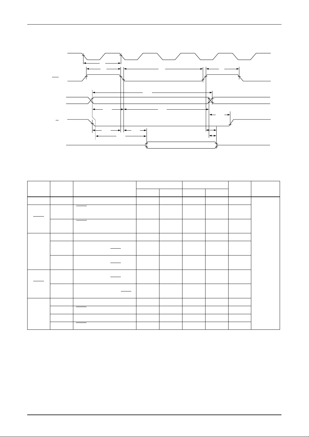
6.3. S1D13305F Timing Diagrams
6.3.1. 8080 family interface timing
AO, CS
t
AW8
WR, RD
t
D0 to D7
(Write)
t
CC
DS8
t
CYC8
t
AH8
t
DH8
t
ACC8
D0 to D7
(Read)
Ta = –20 to 75°C
Signal Symbol Parameter
t
A0, CS
WR, RD
D0 to D7
Note: For memory control and system control commands:
AH8
t
AW8
t
CYC8
t
t
DS8
DH8
t
t
ACC8
t
OH8
t
CYC8
For all other commands:
t
CYC8
Address hold time 10 — 10 — ns
Address setup time 0 — 0 — ns
System cycle time
CC
Strobe pulsewidth 120 — 150 — ns
Data setup time 120 — 120 — ns
Data hold time 5 — 5 — ns
RD access time — 50 — 80 ns
Output disable time 10 50 10 55 ns
= 2tC + tCC + t
= 4tC + tCC + 30
CEA
+ 75 > t
ACV
+ 245
t
OH8
DD
= 4.5 to 5.5V VDD = 2.7 to 4.5V
V
Min. Max. Min. Max.
See note.
—
See note.
Unit Condition
—ns
CL = 100pF
10 EPSON S1D13305 Series
Technical Manual
Page 17
6.3.2. 6800 family interface timing
E
R/W
A0, CS
D0 to D7
(Write)
D0 to D7
(Read)
Note: t
CYC6
indicates the interval during which CS is LOW and E is HIGH.
SPECIFICATIONS
t
CYC6
t
AW6
t
ACC6
t
EW
t
AH6
t
t
DS6
DH6
t
OH6
Ta = –20 to 75°C
DD
= 4.5 to 5.5V VDD = 2.7 to 4.5V
Signal Symbol Parameter
t
A0,
CS,
R/W
D0 to D7
CYC6
t
AW6
t
AH6
t
DS6
t
DH6
t
OH6
t
ACC6
System cycle time
Address setup time 0 — 10 — ns
Address hold time 0 — 0 — ns
Data setup time 100 — 120 — ns
Data hold time 0 — 0 — ns
Output disable time 10 50 10 75 ns
Access time — 85 — 130 ns
V
Min. Max. Min. Max.
See note.
—
See note.
—ns
EtEWEnable pulsewidth 120 — 150 — ns
Note: For memory control and system control commands:
= 2tC + tEW + t
t
CYC6
For all other commands:
= 4tC + tEW + 30
t
CYC6
CEA
+ 75 > t
ACV
+ 245
Unit Condition
CL =
100 pF
S1D13305 Series EPSON 11
Technical Manual
Page 18
SPECIFICATIONS
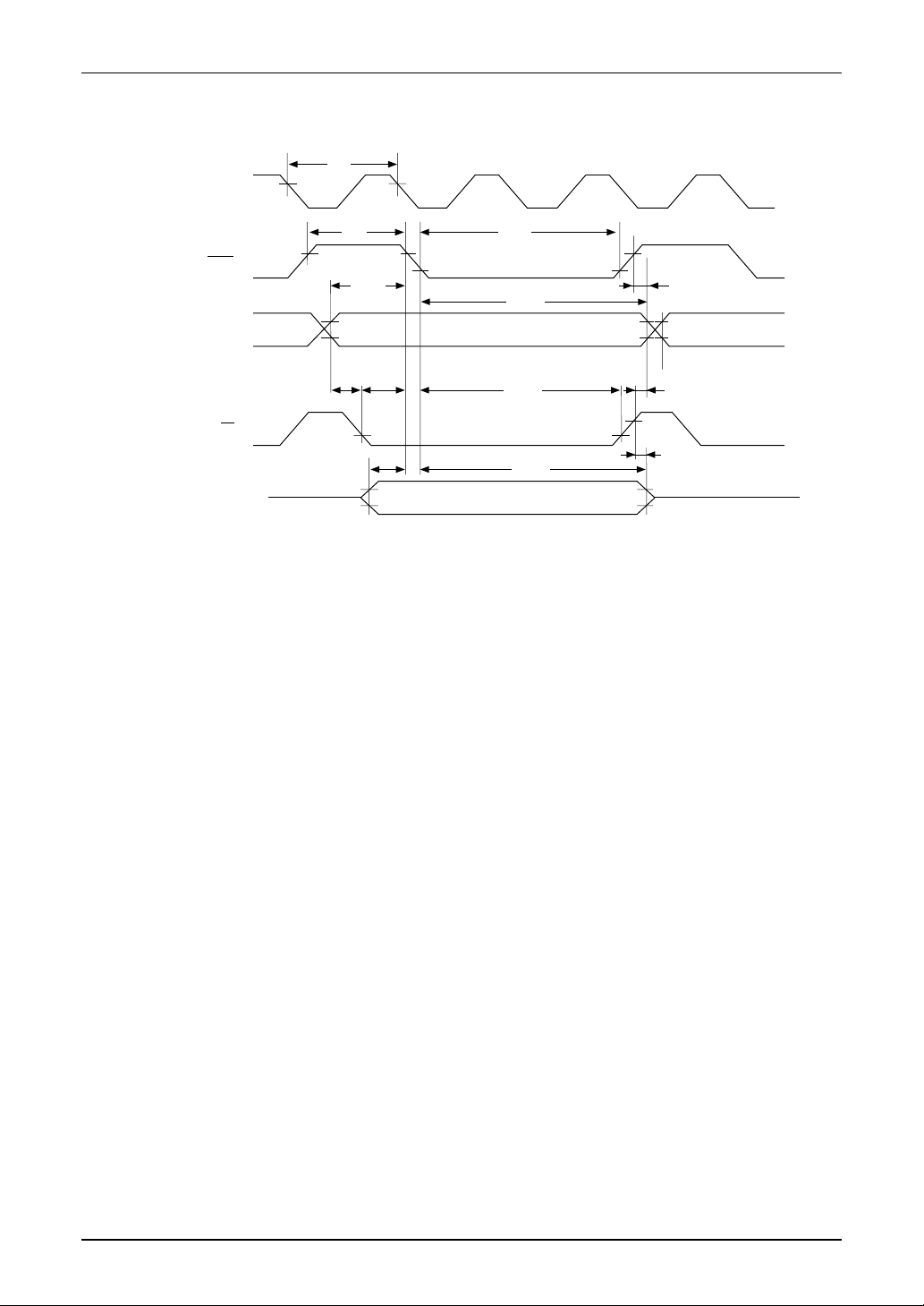
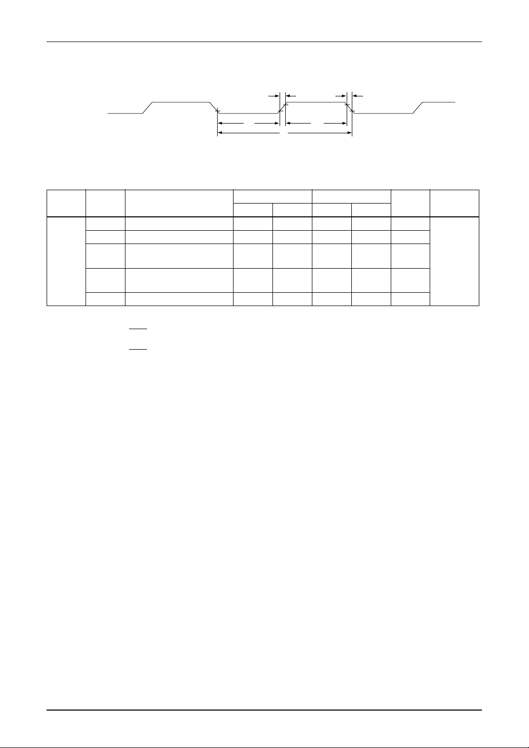
6.3.3. Display memory read timing
EXTΦ0
VCE
VA0 to VA15
VR/W
VD0 to VD7
t
C
t
W
t
ASC
t
RCS
t
CEA
t
ACV
t
CYR
t
t
CE
AHC
t
W
t
RCH
t
CE3
t
OH2
Ta = –20 to 75°C
DD
= 4.5 to 5.5V VDD = 2.7 to 4.5V
Signal Symbol Parameter
V
Min. Max. Min. Max.
EXT φ0tCClock period 100 — 125 — ns
VCE HIGH-level
VCE
VA0 to
VA15
VRD
VD0 to
VD7
t
t
CE
t
CYR
ASC
t
AHC
t
t
RCS
RCH
t
ACV
t
t
CEA
t
OH2
t
CE3
W
pulsewidth
VCE LOW-level
pulsewidth
Read cycle time 3t
Address setup time to
falling edge of VCE
Address hold time from
falling edge of VCE
Read cycle setup time to
falling edge of VCE
Read cycle hold time
from rising edge of VCE
Address access time — 3tC – 100 — 3tC – 115 ns
VCE access time — 2tC – 80 — 2tC – 90 ns
Output data hold time 0 — 0 — ns
VCE to data off time 0 — 0 — ns
C
– 50 — tC – 50 — ns
t
– 30 — 2tC – 30 — ns
2t
C
C
C
– 70 — tC – 100 — ns
t
– 30 — 2tC – 40 — ns
2t
C
t
C
– 45 — tC – 60 — ns
0.5t
—3tC—ns
C
— 0.5t
C
—ns
Unit Condition
CL = 100
pF
12 EPSON S1D13305 Series
Technical Manual
Page 19
6.3.4. Display memory write timing
t
C
EXTφO
SPECIFICATIONS
VCE
VA0 to VA15
VR/W
VD0 to VD7
t
W
t
ASC
t
t
WSC
AS
t
DSC
t
CE
t
AHC
t
WHC
t
DHC
t
t
AH2
DH2
t
CA
S1D13305 Series EPSON 13
Technical Manual
Page 20
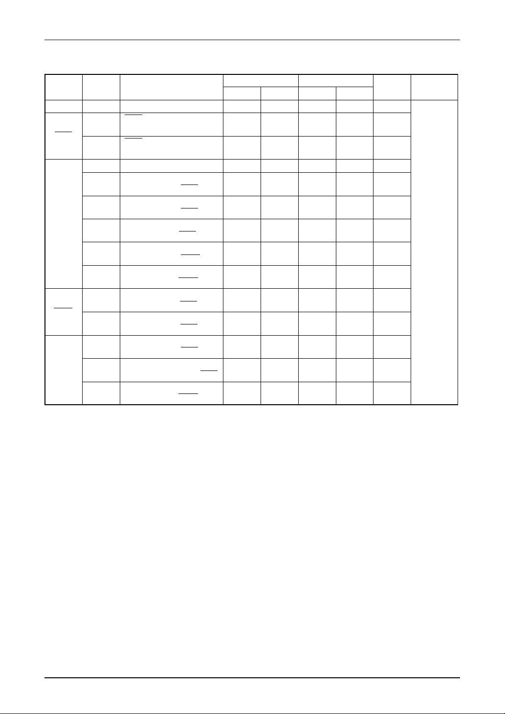
SPECIFICATIONS
Ta = –20 to 75°C
DD
= 4.5 to 5.5V VDD = 2.7 to 4.5V
Signal Symbol Parameter
V
Min. Max. Min. Max.
EXT φ0tCClock period 100 — 125 — ns
VCE HIGH-level
W
t
VCE
t
CYW
t
AHC
t
ASC
t
VA0 to
VA15
t
t
t
t
WSC
VWR
t
WHC
t
DSC
VD0 to
VD7 from falling edge of VCE
Note: VD0 to VD7 are latching input/outputs. While the bus is high impedance, VD0 to VD7 retain the write data until the data read
DHC
t
t
DH2
from the memory is placed on the bus.
pulsewidth
VCE LOW-level
CE
pulsewidth
Write cycle time 3t
Address hold time from
falling edge of VCE
Address setup time to
falling edge of VCE
Address hold time from
CA
rising edge of VCE
Address setup time to
AS
falling edge of VWR
Address hold time from
AH2
rising edge of VWR
Write setup time to
falling edge of VCE
Write hold time from
falling edge of VCE
Data input setup time to
falling edge of VCE
Data input hold time
Data hold time from
rising edge of VWR
C
– 50 — tC – 50 — ns
t
2t
C
– 30 — 2tC – 30 — ns
C
C
– 30 — 2tC – 40 — ns
2t
– 70 — tC – 110 — ns
t
C
—3tC—ns
0—0—ns
0—0—ns
10 — 10 — ns
C
– 80 — tC – 115 — ns
t
– 20 — 2tC – 20 — ns
2t
C
C
– 85 — tC – 125 — ns
t
– 30 — 2tC – 30 — ns
2t
C
550550ns
Unit Condition
CL = 100
pF
14 EPSON S1D13305 Series
Technical Manual
Page 21
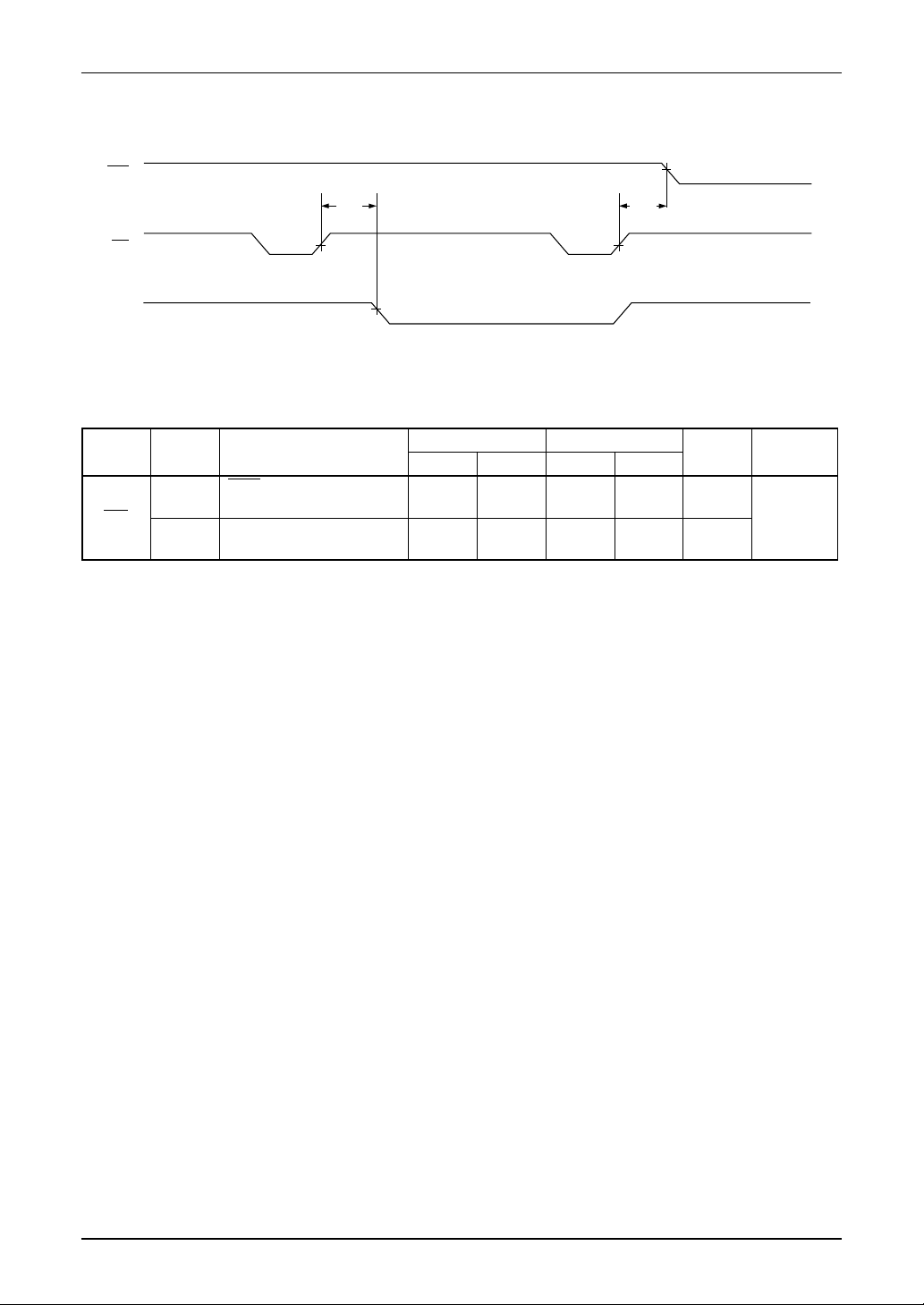
6.3.5. SLEEP IN command timing
SPECIFICATIONS
VCE
WR
(Command input)
YDIS
Ta = –20 to 75°C
Signal Symbol Parameter
VCE falling-edge delay
time
YDIS falling-edge delay
time
OSS
+ 40 (t
is the time delay from the sleep state until stable operation)
OSS
WR
Notes:
1. t
2. t
WRD
t
t
WRL
= 18tC + t
WRD
= 36tC × [TC/R] × [L/F] + 70
WRL
t
WRL
SYSTEM SET writeSLEEP IN write
DD
= 4.5 to 5.5V VDD = 2.7 to 4.5V
V
Min. Max. Min. Max.
See note 1.
—
See note 2.
—
See note 1.
—
t
WRD
Unit Condition
—ns
See note 2.
ns
CL = 100
pF
S1D13305 Series EPSON 15
Technical Manual
Page 22
SPECIFICATIONS
6.3.6. External oscillator signal timing
EXTφ0
Ta = –20 to 75°C
Signal Symbol Parameter
t
EXT φ0
Notes:
1.
2.
RCL
t
FCL
t
t
C
– t
RCL
– t
(t
C
– t
RCL
– t
(t
External clock rise time — 15 — 15 ns
External clock fall time — 15 — 15 ns
External clock
WH
HIGH-level pulsewidth
External clock
WL
LOW-level pulsewidth
C
External clock period 100 — 125 — ns
t
475
FCL
) ×
< tWH, t
FCL
) ×
1000
525
1000
> tWH, t
WL
WL
t
RCL
t
WL
DD
V
t
= 4.5 to 5.5V VDD = 2.7 to 4.5V
t
C
WH
t
FCL
Min. Max. Min. Max
See note 1. See note 2.See note 1. See note 2.
See note 1. See note 2.See note 1. See note 2.
Unit Condition
ns
ns
16 EPSON S1D13305 Series
Technical Manual
Page 23
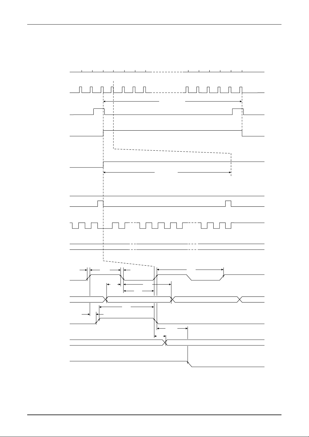
6.3.7. LCD output timing
The following characteristics are for a 1/64 duty cycle.
62 63 64 1 2 3 4 60 61 62 63 64
Row
LP
YD
WF
WF
SPECIFICATIONS
1 frame time
1 line time
Row 64 Row 1
LP
XSCL
XD0 to XD3
(14) (15) (16) (1) (15) (15)(16) (16)(1) (3) (1)(2)
r
t
t
WX
XSCL
t
DS
XD0 to XD3
t
WL
t
LD
LP
WF(B)
YD
Row 2
t
f
t
t
DH
t
LS
t
DHY
t
DF
CX
S1D13305 Series EPSON 17
Technical Manual
Page 24
SPECIFICATIONS
Ta = –20 to 75°C
Signal Symbol Parameter
t
r
Rise time — 30 — 40 ns
f
Fall time — 30 — 40 ns
t
t
CX
XSCL
XD0 to
XD3
LP t
WF t
YD t
t
t
t
t
t
DHY
Shift clock cycle time 4t
WX
XSCL clock pulsewidth 2tC – 60 — 2tC – 60 — ns
DH
X data hold time 2tC – 50 — 2tC – 50 — ns
DS
X data setup time 2tC – 100 — 2tC – 105 — ns
LS
Latch data setup time 2tC – 50 — 2tC – 50 — ns
WL
LP pulsewidth 4tC – 80 — 4tC – 120 — ns
LD
LP delay time from XSCL 0 — 0 — ns
DF
Permitted WF delay — 50 — 50 ns
Y data hold time 2tC – 20 — 2tC – 20 — ns
DD
= 4.5 to 5.5V VDD = 2.7 to 4.5V
V
Min. Max. Min. Max
C
—4tC—ns
Unit Condition
CL =
100 pF
18 EPSON S1D13305 Series
Technical Manual
Page 25
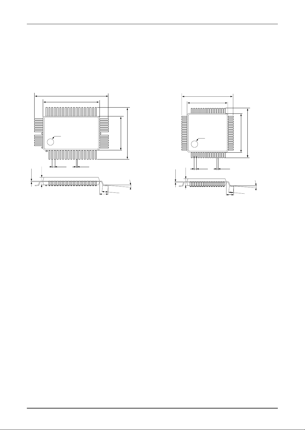
7. PACKAGE DIMENSIONS
Unit: mm
PACKAGE DIMENSIONS
7.1. S1D13305F00A
◊
QFP5-60 pin
0.4
25.6 ±
0.1
20.0 ±
Index
623
0.1
1.0 ±
0.35 ±
55
60
0.05
±
0.15
54
1
5
0.1
±
2.7
7.2. S1D13305F00B
◊
QFP6-60 pin
0.4
17.6 ±
0.2
36
35
0.4
0.1
30
±
±
29
19.6
14.0
24
0.1
46
60
0.1
0.05
±
0.15
1.5 ±
0 to 12°
0.3
2.8
14.0 ±
45
31
30
0.2
±
Index
14.0
16
115
0.35 ±
0.15
0.15
0.8 ±
±
2.7
0.8 ±
0.3
1.8
0.4
±
17.6
0 to 12°
S1D13305 Series EPSON 19
Technical Manual
Page 26
INSTRUCTION SET
8. INSTRUCTION SET
8.1. The Command Set
Table 1. Command set
Code Read
Class Command Hex Command Description
RD WR A0 D7 D6 D5 D4 D3 D2 D1 D0
System
control
Display
control
Drawing
control
Memory
control
Notes:
SYSTEM SET 1010100000040
SLEEP IN 1010101001153Enter standby mode 0 8.2.2
DISP ON/OFF 1010101100D
SCROLL 1010100010044
CSRFORM 101010111015DSet cursor type 2 8.3.3
CGRAM ADR 101010111005C
CSRDIR 101010011
HDOT SCR 101010110105A
OVLAY 101010110115B
CSRW 1010100011046Set cursor address 2 8.4.1
CSRR 1010100011147Read cursor address 2 8.4.2
MWRITE 1010100001042Write to display memory — 8.5.1
MREAD 1010100001143
1. In general, the internal registers of the S1D13305 series are modified as each command parameter is input. However,
the microprocessor does not have to set all the parameters of a command and may send a new command before all parameters
have been input. The internal registers for the parameters that have been input will have been changed but the remaining
parameter registers are unchanged.
2-byte parameters (where two bytes are treated as 1 data item) are handled as follows:
a. CSRW, CSRR: Each byte is processed individually. The microprocessor may read or write just the low byte of the cursor
address.
b. SYSTEM SET, SCROLL, CGRAM ADR: Both parameter bytes are processed together. If the command is changed after
half of the parameter has been input, the single byte is ignored.
2. APL and APH are 2-byte parameters, but are treated as two 1-byte parameters.
CD CD
10tomovement
Initialize device and
display
58, Enable and disable dis59 play and display flashing
Set display start address
and display regions
Set start address of character generator RAM
4C
Set direction of cursor
4F
Set horizontal scroll
position
Set display overlay
format
Read from display
memory
Command
Parameters
No. of SecBytes tion
8 8.2.1
1 8.3.1
10 8.3.2
2 8.3.6
0 8.3.4
1 8.3.7
1 8.3.5
— 8.5.2
20 EPSON S1D13305 Series
Technical Manual
Page 27
8.2. System Control Commands
8.2.1. SYSTEM SET
Initializes the device, sets the window sizes, and selects
the LCD interface format. Since this command sets the
basic operating parameters of the S1D13305 series, an
INSTRUCTION SET
incorrect SYSTEM SET command may cause other
commands to operate incorrectly.
D7 D6 D5 D4 D3 D2 D1 D0 A0 WR RD
C 01000000 1 0 1
P1 0 0 IV 1 W/S M2 M1 M0 0 0 1
P2 WF0000 FX 0 0 1
P3 0000 FY 0 0 1
P4 C/R 0 0 1
P5 TC/R 0 0 1
P6 L/F 0 0 1
P7 APL 0 0 1
P8 APH 0 0 1
LSBMSB
Figure 1. SYSTEM SET instruction
8.2.1.1. C
This control byte performs the following:
1. Resets the internal timing generator
2. Disables the display
3. Cancels sleep mode
Parameters following P1 are not needed if only canceling sleep mode.
Note that if the CG ROM address space overlaps the
display memory address space, that portion of the display
memory cannot be written to.
8.2.1.3. M1
Selects the memory configuration for user-definable characters. The CG RAM codes select one of the 64 codes
8.2.1.2. M0
Selects the internal or external character generator ROM.
The internal character generator ROM contains 160, 5 ×
7 pixel characters, as shown in figure 70. These characters are fixed at fabrication by the metallization mask.
The external character generator ROM, on the other
hand, can contain up to 256 user-defined characters.
M0 = 0: Internal CG ROM
M0 = 1: External CG ROM
S1D13305 Series EPSON 21
Technical Manual
shown in figure 46.
M1 = 0: No D6 correction.
The CG RAM1 and CG RAM2 address spaces are not
contiguous, the CG RAM1 address space is treated as
character generator RAM, and the CG RAM2 address
space is treated as character generator ROM.
M1 = 1: D6 correction.
The CG RAM1 and CG RAM2 address spaces are
contiguout and are both treated as character generator
RAM.
Page 28
INSTRUCTION SET
8.2.1.4. M2
Selects the height of the character bitmaps. Characters
more than 16 pixels high can be displayed by creating a
bitmap for each portion of each character and using the
S1D13305 series graphics mode to reposition them.
M2 = 0: 8-pixel character height (2716 or equivalent
ROM)
M2 = 1: 16-pixel character height (2732 or equivalent
ROM)
EI
YD
Y driver
Figure 2. Single-panel display
8.2.1.5. W/S
Selects the LCD drive method.
W/S = 0: Single-panel drive
W/S = 1: Dual-panel drive
X driver X driver
LCD
YD
Y driver
EI
X driver X driver
Upper Panel
Lower Panel
X driver X driver
Figure 3. Above and below two-panel display
22 EPSON S1D13305 Series
Technical Manual
Page 29
INSTRUCTION SET
EI
YD
Y driver
X driver X driver X driver X driver
Right PanelLeft Panel
Figure 4. Left-and-right two-panel display
Note
There are no Seiko Epson LCD units in the configuration shown in Figure 4.
Table 2. LCD parameters
Parameter
IV = 1 IV = 0 IV = 1 IV = 0
W/S = 0 W/S = 1
C/R C/R C/R C/R C/R
TC/R TC/R TC/R (See note 1.) TC/R TC/R
L/F L/F L/F L/F L/F
SL1 00H to L/F
SL2 00H to L/F
00H to L/F + 1
(See note 2.)
00H to L/F + 1
(See note 2.)
(L/F) / 2 (L/F) / 2
(L/F) / 2 (L/F) / 2
SAD1 First screen block First screen block First screen block First screen block
SAD2 Second screen block Second screen block Second screen block Second screen block
SAD3 Third screen block Third screen block Third screen block Third screen block
SAD4 Invalid Invalid Fourth screen block Fourth screen block
Cursor move-
ment range continuous movement over whole screen
Notes:
1. See table 26 for further details on setting the C/R and TC/R parameters when using the HDOT SCR command.
2. The value of SL when IV = 0 is equal to the value of SL when IV = 1, plus one.
Continuous movement over whole screen
Above-and-below configuration:
8.2.1.6. IV
Screen origin compensation for inverse display. IV is
usually set to 1.
The best way of displaying inverted characters is to
Exclusive-OR the text layer with the graphics back-
left of the screen are difficult to read as the character
origin is at the top-left of its bitmap and there are no
background pixels either above or to the left of these
characters.
ground layer. However, inverted characters at the top or
S1D13305 Series EPSON 23
Technical Manual
Page 30

8 bits
FY
FX
8 bits
FY
FX
Non-display areaAddress BAddress A
8 bits
8 bits
INSTRUCTION SET
The IV flag causes the S1D13305 series to offset the text
screen against the graphics back layer by one vertical
pixel. Use the horizontal pixel scroll function (HDOT
SCR) to shift the text screen 1 to 7 pixels to the right. All
characters will then have the necessary surrounding background pixels that ensure easy reading of the inverted
characters.
See Section 10.5 for information on scrolling.
IV = 0: Screen top-line correction
IV = 1: No screen top-line correction
Display start point
Back layer
HDOT SCR
Character
Dots 1 to 7
IV
1 dot
Figure 5. IV and HDOT SCR adjustment
8.2.1.7. FX
Define the horizontal character size. The character width
in pixels is equal to FX + 1, where FX can range from 00
to 07H inclusive. If data bit 3 is set (FX is in the range 08
to 0FH) and an 8-pixel font is used, a space is inserted
between characters.
Table 3. Horizontal character size selection
FX
HEX D3 D2 D1 D0
[FX] character width
(pixels)
00 0000 1
01 0001 2
↓ ↓↓↓↓ ↓
07 0111 8
Since the S1D13305 series handles display data in 8-bit
units, characters larger than 8 pixels wide must be formed
from 8-pixel segments. As Figure 6 shows, the remainder
of the second eight bits are not displayed. This also
applies to the second screen layer.
In graphics mode, the normal character field is also eight
pixels. If a wider character field is used, any remainder in
the second eight bits is not displayed.
Figure 6. FX and FY display addresses
24 EPSON S1D13305 Series
Technical Manual
Page 31

INSTRUCTION SET
8.2.1.8. WF
Selects the AC frame drive waveform period. WF is
usually set to 1.
WF = 0: 16-line AC drive
WF = 1: two-frame AC drive
In two-frame AC drive, the WF period is twice the frame
period.
In 16-line AC drive, WF inverts every 16 lines.
Although 16-line AC drive gives a more readable display,
horizontal lines may appear when using high LCD drive
voltages or at high viewing angles.
8.2.1.9. FY
Sets the vertical character size. The height in pixels is
equal to FY + 1.
FY can range from 00 to 0FH inclusive.
Set FY to zero (vertical size equals one) when in graphics
mode.
Table 4. Vertical character size selection
FY
HEX D3 D2 D1 D0
00 0000 1
01 0001 2
↓ ↓↓↓↓ ↓
07 0111 8
↓ ↓↓↓↓ ↓
0E1110 15
0F 1111 16
[FY] character
height (pixels)
8.2.1.10. C/R
Sets the address range covered by one display line, that is,
the number of characters less one, multiplied by the
number of horizontal bytes per character.
C/R can range from 0 to 239.
For example, if the character width is 10 pixels, then the
address range is equal to twice the number of characters,
less 2. See Section 16.1.1 for the calculation of C/R.
[C/R] cannot be set to a value greater than the address
range. It can, however, be set smaller than the address
range, in which case the excess display area is blank. The
number of excess pixels must not exceed 64.
Table 5. Display line address range
C/R
HEX D7 D6 D5 D4 D3 D2 D1 D0
00 00000000 1
01 00000001 2
↓ ↓↓↓↓↓↓↓↓ ↓
4F 01001111 80
↓ ↓↓↓↓↓↓↓↓ ↓
EE11101110 239
EF11101111 240
[C/R] bytes per display line
S1D13305 Series EPSON 25
Technical Manual
Page 32

INSTRUCTION SET
8.2.1.11. TC/R
Sets the length, including horizontal blanking, of one
line. The line length is equal to TC/R + 1, where TC/ R can
range from 0 to 255.
TC/R must be greater than or equal to C/R + 4. Provided
this condition is satisfied, [TC/R] can be set according to
Table 6. Line length selection
TC/R
HEX D7 D6 D5 D4 D3 D2 D1 D0
00 00000000 1
01 00000001 2
↓ ↓↓↓↓↓↓↓↓ ↓
52 01010010 83
↓ ↓↓↓↓↓↓↓↓ ↓
FE11111110 255
FF 11111111 256
8.2.1.12. L/F
Sets the height, in lines, of a frame. The height in lines is
equal to L/F + 1, where L/F can range from 0 to 255.
the equation given in section 16.1.1 in order to hold the
frame period constant and minimize jitter for any given
main oscillator frequency, f
[TC/R] line length (bytes)
OSC.
Table 7. Frame height selection
L/F
HEX D7 D6 D5 D4 D3 D2 D1 D0
00 00000000 1
01 00000001 2
↓ ↓↓↓↓↓↓↓↓ ↓
7F 01111111 128
↓ ↓↓↓↓↓↓↓↓ ↓
FE11111110 255
FF 11111111 256
[L/F] lines per frame
If W/S is set to 1, selecting two-screen display, the
number of lines must be even and L/F must, therefore, be
an odd number.
26 EPSON S1D13305 Series
Technical Manual
Page 33

8.2.1.13. AP
Defines the horizontal address range of the virtual screen.
APL is the least significant byte of the address.
APL AP7 AP6 AP5 AP4 AP3 AP2 AP1 AP0
APH AP15 AP14 AP13 AP12 AP11 AP10 AP9 AP8
Figure 7. AP parameters
Table 8. Horizontal address range
Hex code
APH APL
[AP] addresses
per line
0000 0
0001 1
↓↓↓↓ ↓
0050 80
↓↓↓↓ ↓
FFFE 216 – 2
FFFF 216 – 1
INSTRUCTION SET
Blank data is sent to the X-drivers, and the Y-drivers have
their bias supplies turned off by the YDIS signal. Using
the YDIS signal to disable the Y-drivers guards against
any spurious displays.
The internal registers of the S1D13305 series maintain
their values during the sleep state. The display memory
control pins maintain their logic levels to ensure that the
display memory is not corrupted.
The S1D13305 series can be removed from the sleep state
by sending the SYSTEM SET command with only the P1
parameter. The DISP ON command should be sent next
to enable the display.
MSB LSB
C01010011
Display area
C/R
Display memory limit
AP
Figure 8. AP and C/R relationship
8.2.2. SLEEP IN
Places the system in standby mode. This command has no
parameter bytes. At least one blank frame after receiving
this command, the S1D13305F halts all internal operations, including the oscillator, and enters the sleep state.
Figure 9. SLEEP IN instruction
1. The YDIS signal goes LOW between one and two
frames after the SLEEP IN command is received.
Since YDIS forces all display driver outputs to go to
the deselected output voltage, YDIS can be used as a
power-down signal for the LCD unit. This can be
done by having YDIS turn off the relatively highpower LCD drive supplies at the same time as it
blanks the display.
2. Since all internal clocks in the S1D13305 series are
halted while in the sleep state, a DC voltage will be
applied to the LCD panel if the LCD drive supplies
remain on.
If reliability is a prime consideration, turn off the
LCD drive supplies before issuing the SLEEP IN
command.
3. Note that, although the bus lines become high impedance in the sleep state, pull-up or pull-down resistors
on the bus will force these lines to a known state.
S1D13305 Series EPSON 27
Technical Manual
Page 34

INSTRUCTION SET
8.3. Display Control Commands
8.3.1. DISP ON/OFF
Turns the whole display on or off. The single-byte parameter enables and disables the cursor and layered screens,
and sets the cursor and screen flash rates. The cursor can
be set to flash over one character or over a whole line.
8.3.1.3. FP
Each pair of bits in FP sets the attributes of one screen
block, as follows.
The display attributes are as follows:
MSB LSB
C0101100D
P1 FP5 FP4 FP3 FP2 FP1 FP0 FC1 FC0
Figure 10. DISP ON/OFF parameters
8.3.1.1. D
Turns the display ON or OFF. The D bit takes precedence over the FP bits in the parameter.
D = 0: Display OFF
D = 1: Display ON
8.3.1.2. FC
Enables/disables the cursor and sets the flash rate. The
cursor flashes with a 70% duty cycle (ON/OFF).
Table 9. Cursor flash rate selection
FC1 FC0 Cursor display
0 0 OFF (blank)
0 1 No flashing
FR
10
ON
11
Note: As the MWRITE command always enables the cursor,
the cursor position can be checked even when performing consecutive writes to display memory while the
cursor is flashing.
Flash at f
(approx. 2 Hz)
Flash at f
(approx. 1 Hz)
/32 Hz
FR
/64 Hz
Table 10. Screen block attribute selection
FP1 FP0 First screen block (SAD1)
FP3 FP2
Second screen block (SAD2,
SAD4). See note.
FP5 FP4 Third screen block (SAD3)
0 0 OFF (blank)
0 1 No flashing
10
11
ON
Flash at f
Flash at f
(approx. 16 Hz)
FR
/32 Hz
(approx. 2 Hz)
FR
/4 Hz
Note
If SAD4 is enabled by setting W/S to 1, FP3 and FP2
control both SAD2 and SAD4. The attributes of
SAD2 and SAD4 cannot be set independently.
28 EPSON S1D13305 Series
Technical Manual
Page 35

8.3.2. SCROLL
8.3.2.1. C
Sets the scroll start address and the number of lines per
scroll block. Parameters P1 to P10 can be omitted if not
MSB LSB
C01000100
P1 A7 A6 A5 A4 A3 A2 A1 A0 (SAD 1L)
P2 A15 A14 A13 A12 A11 A10 A9 A8 (SAD 1H)
P3 L7 L6 L5 L4 L3 L2 L1 L0 (SL 1)
P4 A7 A6 A5 A4 A3 A2 A1 A0 (SAD 2 L)
P5 A15 A14 A13 A12 A11 A10 A9 A8 (SAD 2H)
P6 L7 L6 L5 L4 L3 L2 L1 L0 (SL 2)
P7 A7 A6 A5 A4 A3 A2 A1 A0 (SAD 3L)
INSTRUCTION SET
required. The parameters must be entered sequentially as
shown in Figure 11.
P8 A15 A14 A13 A12 A11 A10 A9 A8 (SAD 3H)
P9 A7 A6 A5 A4 A3 A2 A1 A0 (SAD 4L)
P10 A15 A14 A13 A12 A11 A10 A9 A8 (SAD 4H)
Figure 11. SCROLL instruction parameters
Note: Set parameters P9 and P10 only if both two-screen
drive (W/S = 1) and two-layer configuration are selected. SAD4 is the fourth screen block display start
address.
S1D13305 Series EPSON 29
Technical Manual
Page 36

y
INSTRUCTION SET
Table 11. Screen block start address selection
SL1, SL2
HEX L7 L6 L5 L4 L3 L2 L1 L0
[SL] screen lines
00 00000000 1
01 00000001 2
↓ ↓↓↓↓↓↓↓↓ ↓
7F 01111111 128
↓ ↓↓↓↓↓↓↓↓ ↓
FE11111110 255
FF 11111111 256
8.3.2.2. SL1, SL2
SL1 and SL2 set the number of lines per scrolling screen.
The number of lines is SL1 or SL2 plus one. The relation-
ship between SAD, SL and the display mode is described
below.
Table 12. Text display mode
W/S Screen First Layer Second Layer
First screen block SAD1 SAD2
Second screen block SL1 SL2
SAD3 (see note 1)
Third screen block (partitioned screen) Set both SL1 and SL2 to L/F + 1
if not using a partitioned screen.
Screen configuration example:
SAD2
0
SAD1
SL1
SAD3
Character display page 1
Character display page 3
SL2
Graphics display page 2
Layer 2
er 1
La
30 EPSON S1D13305 Series
Technical Manual
Page 37

y
INSTRUCTION SET
Table 12. Text display mode (continued)
W/S Screen First Layer Second Layer
Upper screen
Lower screen
Set both SL1 and SL2 to ((L/F) / 2 + 1).
Screen configuration example:
SAD2
SAD1
1
SL1
Character display page 1
Graphics display page 2
SAD1 SAD2
SL1 SL2
SAD3 SAD4
(See note 2.) (See note 2.)
SAD3
Character display page 3
La
er 2Layer 1
Notes:
1. SAD3 has the same value as either SAD1 or SAD2, whichever has the least number of lines (set by SL1 and SL2).
2. Since the parameters corresponding to SL3 and SL4 are fixed by L/F, they do not have to be set in this mode.
Graphics display page 4
(SAD4)
S1D13305 Series EPSON 31
Technical Manual
Page 38

INSTRUCTION SET
Table 13. Graphics display mode
W/S Screen First Layer Second Layer Third Layer
Two-layer composition
Upper screen
SAD2
SAD1 SAD2
SL1 SL2
SAD3 (see note 3.)
Set both SL1 and SL2 to
L/F + 1 if not using a
partitioned screen
Screen configuration example:
—
—
0
SAD1
SL1
SAD3
Three-layer configuration
Character display page 1
Character display page 3
Layer 1 Layer 2
SAD1 SAD2 SAD3
SL1 = L/F + 1 SL2 = L/F + 1 —
SL2
Graphics display page 2
Screen configuration example:
SAD3
SAD2
SAD1
0
SL1
Graphics display page 1
Graphics display page 3
SL2
Graphics display page 2
Layer 1
Layer 3
Layer 2
32 EPSON S1D13305 Series
Technical Manual
Page 39

INSTRUCTION SET
Table 13. Graphics display mode (continued)
W/S Screen First Layer Second Layer Third Layer
Upper screen
Lower screen
Set both SL1 and SL2 to ((L/F) / 2 + 1).
Screen configuration example (See note 3.):
SAD2
SAD1
1
SL1
Graphics display page 1
SAD1 SAD2
SL1 SL2
SAD3 SAD4
(See note 2.) (See note 2.)
Graphics display page 2
—
—
SAD3
Graphics display page 3
Layer 2Layer 1
Notes:
1. SAD3 has the same value as either SAD1 or SAD2, whichever has the least number of lines (set by SL1 and SL2).
2. Since the parameters corresponding to SL3 and SL4 are fixed by L/F, they do not have to be set.
3. If, and only if, W/S = 1, the differences between SL1 and (L/F + 1) / 2, and between SL2 and (L/F + 1) / 2, are blanked.
SL1
L
L/2
Upper Panel
Lower Panel
Graphics display page 4
Graphics
Figure 12. Two-panel display height
S1D13305 Series EPSON 33
Technical Manual
Page 40

10
11
0001
–1 +1
+AP
–AP
INSTRUCTION SET
8.3.3. CSRFORM
Sets the cursor size and shape. Although the cursor is
normally only used in text displays, it may also be used in
graphics displays when displaying special characters.
MSB LSB
C01011101
P10000
P2 CM 0 0 0
Figure 13. CSRFORM parameter bytes
8.3.3.1. CRX
Sets the horizontal size of the cursor from the character
origin. CRX is equal to the cursor size less one. CRX must
be less than or equal to FX.
Table 14. Horizontal cursor size selection
CRX
HEX X3 X2 X1 X0
0 0000 1
1 0001 2
↓ ↓↓↓↓ ↓
4 0100 9
↓ ↓↓↓↓ ↓
E 1110 15
F 1111 16
CRX
X3 X2
Y3 Y2
CRY
X1 X0
Y1 Y0
[CRX] cursor width
(pixels)
Character start point
0123456•• •
0
1
2
3
4
5
6
7
8
9
CRX = 5 dots
CRY = 9 dots
CM = 0
Figure 14. Cursor size and position
8.3.3.3. CM
Sets the cursor shape. Always set CM to 1 when in
graphics mode.
CM = 0: Underscore cursor
CM = 1: Block cursor
8.3.4. CSRDIR
Sets the direction of automatic cursor increment. The
cursor can move left or right one character, or up or down
by the number of bytes specified by the address pitch, AP.
When reading from and writing to display memory, this
automatic cursor increment controls the display memory
address increment on each read or write.
8.3.3.2. CRY
Sets the location of an underscored cursor in lines, from
MSB LSB
C010011CD1CD2
the character origin. When using a block cursor, CRY sets
the vertical size of the cursor from the character origin.
CRY is equal to the number of lines less one.
Figure 15. CSRDIR parameters
Table 15. Cursor height selection
CRY
HEX Y3 Y2 Y1 Y0
[CRY] cursor height
(lines)
0 0000 Illegal
1 0001 2
↓ ↓↓↓↓ ↓
8 1000 9
↓ ↓↓↓↓ ↓
E 1110 15
F 1111 16
Figure 16. Cursor direction
34 EPSON S1D13305 Series
Technical Manual
Page 41

Table 16. Cursor shift direction
C CD1 CD0 Shift direction
4CH 0 0 Right
4DH 0 1 Left
4EH 1 0 Up
4FH 1 1 Down
Note: Since the cursor moves in address units even if FX ≥ 9,
the cursor address increment must be preset for movement in character units. See Section 9.3.
8.3.5. OVLAY
Selects layered screen composition and screen text/ graphics mode.
MSB LSB
C01011011
P1 0 0 0 OV DM2 DM1 MX1 MX0
Figure 17. OVLAY parameters
8.3.5.1. MX0, MX1
MX0 and MX1 set the layered screen composition method,
which can be either OR, AND, Exclusive-OR or PriorityOR. Since the screen composition is organized in layers
and not by screen blocks, when using a layer divided into
two screen blocks, different composition methods cannot
be specified for the individual screen blocks.
The Priority-OR mode is the same as the OR mode unless
flashing of individual screens is used.
INSTRUCTION SET
Table 17. Composition method selection
MX1 MX0 Function Composition Method Applications
0 0 L1 ∪ L2 ∪ L3 OR Underlining, rules, mixed text and graphics
0 1 (L1 ⊕ L2) ∪ L3 Exclusive-OR
1 0 (L1 ∩ L2) ∪ L3 AND
1 1 L1 > L2 > L3 Priority-OR
Notes:
L1: First layer (text or graphics). If text is selected, layer L3 cannot be used.
L2: Second layer (graphics only)
L3: Third layer (graphics only)
S1D13305 Series EPSON 35
Technical Manual
Inverted characters, flashing regions,
underlining
Simple animation, three-dimensional
appearance
Page 42

INSTRUCTION SET
Layer 1 Layer 2 Layer 3
1
EPSON
2 Exclusive OR
EPSON
3 AND
EPSON
4 Prioritized OR
EPSON
Figure 18. Combined layer display
Notes:
L1: Not flashing
L2: Flashing at 1 Hz
L3: Flashing at 2 Hz
8.3.5.2. DM1, DM2
DM1 and DM2 specify the display mode of screen blocks
1 and 3, respectively.
DM1/2 = 0: Text mode
DM1/2 = 1: Graphics mode
Note 1: Screen blocks 2 and 4 can only display graphics.
Note 2: DM1 and DM2 must be the same, regardless of
the setting of W/S.
Visible display
EPSON
OR
EPSON
SON
EPSON
8.3.5.3. OV
Specifies two- or three-layer composition in graphics
mode.
OV = 0: Two-layer composition
OV = 1: Three-layer composition
Set OV to 0 for mixed text and graphics mode.
8.3.6. CGRAM ADR
Specifies the CG RAM start address.
MSB LSB
C01011100
P1 A7 A6 A5 A4 A3 A2 A1 A0 (SAGL)
P2 A15 A14 A13 A12 A11 A10 A9 A8 (SAGH)
Figure 19. CGRAM ADR parameters
Note
See section 10 for information on the SAG parameters.
36 EPSON S1D13305 Series
Technical Manual
Page 43

INSTRUCTION SET
8.3.7. HDOT SCR
While the SCROLL command only allows scrolling by
characters, HDOT SCR allows the screen to be scrolled
horizontally by pixels. HDOT SCR cannot be used on
individual layers.
MSB LSB
C01011010
P1 0 0 0 0 0 D2 D1 D0
Figure 20. HDOT SCR parameters
8.3.7.1. D0 to D2
Specifies the number of pixels to scroll. The C/R parameter has to be set to one more than the number of
horizontal characters before using HDOT SCR. Smooth
scrolling can be simulated if the controlling microprocessor repeatedly issues the HDOT SCR command to the
S1D13305 series. See Section 9.5 for more information
on scrolling the display.
Table 18. Scroll step selection (continued)
P1
HEX D2 D1 D0
Number of pixels
to scroll
00 000 0
01 001 1
02 010 2
↓ ↓↓↓ ↓
06 110 6
07 111 7
M
BXY
A
AB XYZ
ZAB XY
Display width N
M/N is the number of bits (dots) that parameter 1 (P1)
is incremented/decremented by.
Figure 21. Horizontal scrolling
M = 0
N = 0
8.4. Drawing Control Commands
8.4.1. CSRW
The 16-bit cursor address register contains the display
memory address of the data at the cursor position as
shown in Figure 22.
Note that the microprocessor cannot directly access the
display memory.
MSB LSB
C01000110
P1 A7 A6 A5 A4 A3 A2 A1 A0 (CSRL)
P2 A15 A14 A13 A12 A11 A10 A9 A8 (CSRH)
Figure 22. CSRW parameters
The MREAD and MWRITE commands use the address
in this register.
S1D13305 Series EPSON 37
Technical Manual
Page 44

INSTRUCTION SET
The cursor address register can only be modified by the
CSRW command, and by the automatic increment after
an MREAD or MWRITE command. It is not affected by
display scrolling.
8.4.2. CSRR
Reads from the cursor address register. After issuing the
command, the data read address is read twice, for the low
byte and then the high byte of the register.
MSB LSB
C01000111
P1 A7 A6 A5 A4 A3 A2 A1 A0 (CSRL)
P2 A15 A14 A13 A12 A11 A10 A9 A8 (CSRH)
Figure 23. CSRR parameters
8.5. Memory Control Commands
8.5.1. MWRITE
The microprocessor may write a sequence of data bytes
to display memory by issuing the MREAD command and
then writing the bytes to the S1D13305 series. There is no
need for further MWRITE commands or for the micro-
If a new address is not set, display memory accesses will
be from the last set address or the address after previous
automatic increments.
processor to update the cursor address register after each
byte as the cursor address is automatically incremented
by the amount set with CSRDIR, in preparation for the
next data write.
MSB LSB
C01000010
P1
P2
Pn n ≥ 1
Figure 24. MWRITE parameters
Note:
P1, P2, ..., Pn: display data.
38 EPSON S1D13305 Series
Technical Manual
Page 45

8.5.2. MREAD
Puts the S1D13305 series into the data output state.
Each time the microprocessor reads the buffer, the cursor
address is incremented by the amount set by CSRDIR and
the next data byte fetched from memory, so a sequence of
MSB LSB
C01000011
P1
P2
Pn n ≥ 1
Figure 25. MREAD parameters
INSTRUCTION SET
data bytes may be read without further MREAD commands or by updating the cursor address register.
If the cursor is displayed, the read data will be from two
positions ahead of the cursor.
S1D13305 Series EPSON 39
Technical Manual
Page 46

DISPLAY CONTROL FUNCTIONS
9. DISPLAY CONTROL FUNCTIONS
9.1. Character Configuration
The origin of each character bitmap is in the top left
corner as shown in Figure 29. Adjacent bits in each byte
are horizontally adjacent in the corresponding character
image.
Character starting point
Character
height
FY
Space
Character width Space
Although the size of the bitmap is fixed by the character
generator, the actual displayed size of the character field
can be varied in both dimensions.
D7 to D0FX
0
R0
R1
R2
R3
R4
R5
R6
R7
R8
R9
R10
R11
R12
R13
R14
R15
1
1
1
0
0
0
0
1
0
0
0
1
0
0
0
1
0
0
0
1
0
0
0
1
0
0
0
1
0
0
0
1
1
1
1
1
0
0
0
1
0
0
0
1
0
0
0
1
0
0
0
1
0
0
0
0
0
0
0
0
0
0
0
0
0
0
0
0
0
0
0
0
0
0
0
0
0
0
0
0
0
0
0
0
0
0
0
0
0
0
0
0
0
0
0
0
0
0
0
0
0
0
0
0
0
0
0
0
0
0
0
0
0
0
0
0
0
0
0
0
0
0
Space
data
Space
0
data
0
0
0
0
Figure 26. Example of character display ([FX] ≤ 8) and generator bitmap
If the area outside the character bitmap contains only
zeros, the displayed character size can easily be increased
by increasing FX and FY, as the zeros ensure that the
The displayed character width can be set to any value up
to 16 even if each horizontal row of the bitmap is two
bytes wide.
extra space between displayed characters is blank.
40 EPSON S1D13305 Series
Technical Manual
Page 47

FY
FX
DISPLAY CONTROL FUNCTIONS
Horizontal
non-display
area
Character
Height
16 dots
Space
Vertical
non-display
area
8 dots 8 dots
SpaceCharacter width
Figure 27. Character width greater than one byte wide ([FX] = 9)
Note: The S1D13305 series does not automatically insert spaces between characters. If the displayed character size is
8 pixels or less and the space between character origins is nine pixels or more, the bitmap must use two bytes per row,
even though the character image requires only one.
S1D13305 Series EPSON 41
Technical Manual
Page 48

DISPLAY CONTROL FUNCTIONS
9.2. Screen Configuration
9.2.1. Screen configuration
The basic screen configuration of the S1D13305 series is
as a single text screen or as overlapping text and graphics
screens. The graphics screen uses eight times as much
display memory as the text screen.
Figure 28 shows the relationship between the virtual
screens and the physical screen.
0000H
0800H
Display
memory
window
Y
(0,0)
(0,YM)
(X,Y)
X
Figure 28. Virtual and physical screen relationship
9.2.2. Display address scanning
The S1D13305 series scans the display memory in the
same way as a raster scan CRT screen. Each row is
scanned from left to right until the address range equals
C/R. Rows are scanned from top to bottom.
In graphics mode, at the start of each line, the address
counter is set to the address at the start of the previous line
plus the address pitch, AP.
C/R
A/P
Character
memory area
07FFH
47FFH
(XW,YM)
(XM,0)
(XM,YM)
Graphics
memory area
In text mode, the address counter is set to the same start
address, and the same character data is read, for each row
in the character bitmap. However, a new row of the
character generator output is used each time. Once all the
rows in the character bitmap have been displayed, the
address counter is set to the start address plus AP and the
next line of text is displayed.
42 EPSON S1D13305 Series
Technical Manual
Page 49

1
•
•
•
8
9
•
•
•
16
17
•
•
•
24
•
•
•
•
SAD
SAD + AP
SAD + 2AP
SAD + 1
SAD + AP
+ 1
SAD + 2
SAD + AP
+ 2
DISPLAY CONTROL FUNCTIONS
SAD + C/R
SAD + AP
+ C/R
SAD
1
SAD + AP
2
SAD + 2AP
3
•
•
•
•
•
•
•
•
W/S = 0, FX = 8
SAD +1
SAD + AP
+ 1
W/S = 0, FX = 8, FY = 8
C/R
Figure 29. Character position parameters
Note: One byte of display memory corresponds to one character.
SAD + 2
SAD + AP
+ 2
C/R
SAD + C/R
SAD + AP
+ C/R
Line 1
Line 2
Line 3
SAD
SAD +1
SAD + 2
AP
SAD + C/R
SAD + AP
SAD + AP + 1
AP
SAD + AP + C/R
SAD + 2AP
Figure 30. Character parameters vs. memory
Note: One bit of display memory corresponds to one pixel.
S1D13305 Series EPSON 43
Technical Manual
Page 50

DISPLAY CONTROL FUNCTIONS
1
SAD1 SAD1 + 1 SAD1 + 2 SAD1 + C/R
•
•
•
8
9
16
17
24
25
(L/F)/2 = β
β + 1
β + 8
β + 9
β + 16
β + 17
β + 24
β + 25
(L/F)
SAD1 + AP SAD1 + AP
•
•
•
SAD1 + 2AP
•
•
•
•
•
•
SAD3 + 1 SAD3 + 2 SAD3 + C/R
•
•
•
SAD3 + AP SAD3 + AP
•
•
•
SAD3 + 2AP
•
•
•
•
•
•
•
W/S = 1, FX = 8, FY = 8
+ 1
+ 1
SAD1 + AP
+ 2
SAD3 + AP
+ 2
C/R
SAD1 + AP
+ C/R
SAD3 + AP
+ C/R
Figure 31. Two-panel display address indexing
Note
In two-panel drive, the S1D13305 series reads line 1 and line β + 1 as one cycle. The upper and lower panels
are thus read alternately, one line at a time.
44 EPSON S1D13305 Series
Technical Manual
Page 51

9.2.3. Display scan timing
Figure 32 shows the basic timing of the S1D13305 series.
One display memory read cycle takes nine periods of the
system clock, φ0 (
times per display line.
When reading, the display memory pauses at the end of
each line for (TC/R - C/R) display memory read cycles,
φ0
VCE
VA
fOSC ). This cycle repeats (C/R + 1)
T0 T1 T2
Figure 32. Display memory basic read cycle
Display read cycle interval
Graphics read intervalCharacter read interval
DISPLAY CONTROL FUNCTIONS
though the LCD drive signals are still generated. TC/R
may be set to any value within the constraints imposed by
fOSC , fFR , and the size of the LCD panel, and it may
C/R,
be used to fine tune the frame frequency. The microprocessor may also use this pause to access the display
memory data.
Character generator
read interval
Frame
period
Line 1
Display period Divider frequency
TC/R
C/R
O
2
3
O
O
•
period
R
R
R
•
•
•
(L/F)
LP
Figure 33. Relationship between TC/R and C/R
Note: The divider adjustment interval (R) applies to both the upper and lower screens even if W/S = 1. In this case, LP is active
only at the end of the lower screen’s display interval.
•
O
R
S1D13305 Series EPSON 45
Technical Manual
Page 52

DISPLAY CONTROL FUNCTIONS
9.3. Cursor Control
9.3.1. Cursor register function
The S1D13305 series cursor address register functions as
both the displayed cursor position address register and
the display memory access address register. When accessing display memory outside the actual screen memory,
the address register must be saved before accessing the
memory and restored after memory access is complete.
Although the cursor is normally displayed for character
data, the S1D13305 series may also display a dummy
cursor for graphical characters. This is only possible if the
graphics screen is displayed, the text screen is turned off
and the microprocessor generates the cursor control address.
Cursor display
address register
Cursor register
Address pointer
Figure 34. Cursor addressing
Note that the cursor may disappear from the display if the
cursor address remains outside the displayed screen
memory for more than a few hundred milliseconds.
9.3.2. Cursor movement
On each memory access, the cursor address register
changes by the amount previously specified with CSRDIR,
automatically moving the cursor to the desired location.
9.3.3. Cursor display layers
Although the S1D13305 series can display up to three
layers, the cursor is displayed in only one of these layers:
Two-layer configuration: First layer (L1)
Three-layer configuration: Third layer (L3)
The cursor will not be displayed if it is moved outside the
memory for its layer. Layers may be swapped or the
cursor layer moved within the display memory if it is
necessary to display the cursor on a layer other than the
present cursor layer.
D = 1
FC1 = 0
FC0 = 1
FP1 = 0
FP0 = 0
FP3 = 0
FP2 = 1
Cursor ON
Block screen 1 (character
screen) OFF
Block screen 2 (graphics
screen) ON
Figure 35. Cursor display layers
Consider the example of displaying Chinese characters
on a graphics screen. To write the display data, the cursor
address is set to the second screen block, but the cursor is
not displayed. To display the cursor, the cursor address is
set to an address within the blank text screen block.
Since the automatic cursor increment is in address units,
not character units, the controlling microprocessor must
set the cursor address register when moving the cursor
over the graphical characters.
46 EPSON S1D13305 Series
Technical Manual
Page 53

DISPLAY CONTROL FUNCTIONS
18 dots
Auto shift
8 dots8 dots8 dots8 dots
Auto shift Auto shift
Cursor address preset
Block cursor
Figure 36. Cursor movement
If no text screen is displayed, only a bar cursor can be
displayed at the cursor address.
If the first layer is a mixed text and graphics screen and the
cursor shape is set to a block cursor, the S1D13305 series
automatically decides which cursor shape to display. On
the text screen it displays a block cursor, and on the
graphics screen, a bar cursor.
S1D13305 Series EPSON 47
Technical Manual
Page 54

DISPLAY CONTROL FUNCTIONS
9.4. Memory to Display Relationship
The S1D13305 series supports virtual screens that are
larger than the physical size of the LCD panel address
range, C/R. A layer of the S1D13305 series can be
considered as a window in the larger virtual screen held
in display memory. This window can be divided into two
blocks, with each block able to display a different portion
of the virtual screen.
This enables, for example, one block to dynamically
scroll through a data area while the other acts as a status
message display area. See Figure 37 and 38.
W/S = 0 W/S = 1
Display page 1
Layer 1
Display page 2
Layer 2
SAD1
SAD3
SAD2
Display page 1
Layer 1
Display page 2
Layer 2
SAD1
SAD3
SAD3Display page 3
SAD3
C/R
Character page 1
Character page 3
SAD2
Graphics page 2
SAD4
Graphics page 2
SAD1
Character page 1
C/R
Character page 3
SAD2
C/R
Graphics page 3
AP
SAD1
SAD3
SAD2
SAD4
C/R
CG RAM
C/R
C/R
Graphics page 2
Display page 1
Display page 3
Layer 1
Display page 2
Display page 4
Layer 2
C/R
Graphics page 2
SAD1
Graphics page 1
C/R
SAD1
SAD3
SAD2
Layer 1
Display page 3
Display page 2
Display page 1
Layer 2
SAD2
Layer 3
Figure 37. Display layers and memory
48 EPSON S1D13305 Series
Technical Manual
Page 55

DISPLAY CONTROL FUNCTIONS
0000H
SAD1
L/F
FX = Horizontal character field ≤ 16 dots
FY = Vertical character field ≤ 16 dots
CRX = Horizontal cursor size ≤ 16 dots
CRY = Vertical cursor size ≤ 16 dots
C/R = Characters per row ≤ 240 bytes
L/F = Lines per frame ≤ 256 bytes
AP = Address pitch ≤ 64 Kbytes
FX
FY
CSRA CRX
CRY
C/R
AP
Display
window
Virtual display
memory limit
FFFFH
Figure 38. Display window and memory
S1D13305 Series EPSON 49
Technical Manual
Page 56

DISPLAY CONTROL FUNCTIONS
XY
D0
(LSB)
βα
D7 to D0 D7 to D0
ABC
0000
A (Code)BC
Page 1
Page 2
Display
X
02FF
Y
Page 1
0080
α
D0 D7
(LSB)(MSB)
(MSB)
D7
β
γ
Page 2
1FFF
χ
HEX D7 D0
RAM
Not used
Character generator
Magnified image
12345
#4800
01110000
10001000
10001000
10001000
11111000
10001000
70888888F88888
ROM
Character generator
6
#4807
10001000
00000000
00
Example of character A
0000
SAD1
SL1
0300
0400
code
Character
0800
SAD2
SL2
2000
2800
Back layer
4440
SAG
4800
4A00
F000
Figure 39. Memory map and magnified characters
50 EPSON S1D13305 Series
Technical Manual
Page 57

9.5. Scrolling
The controlling microprocessor can set the S1D13305
series scrolling modes by overwriting the scroll address
registers SAD1 to SAD4, and by directly setting the
scrolling mode and scrolling rate.
9.5.1. On-page scrolling
The normal method of scrolling within a page is to move
the whole display up one line and erase the bottom line.
DISPLAY CONTROL FUNCTIONS
Since the S1D13305 series does not automatically erase
the bottom line, it must be erased with blanking data when
changing the scroll address register.
Display memory
AP
C/R
Before scrolling
After scrolling
ABC
WXYZ 789
WXYZ 789
Blank
Figure 40. On-page scrolling
9.5.2. Inter-page scrolling
Scrolling between pages and page switching can be
performed only if the display memory capacity is greater
than one screen.
Before scrolling
ABC
WXYZ 789
SAD1
SAD3
SAD1
SAD1
ABC
WXYZ 789
Blank
WXYZ 789
Display memory
AP
C/R
ABC
WXYZ 789
After scrolling
WXYZ 789
SAD1
ABC
WXYZ 789
Figure 41. Inter-page scrolling
S1D13305 Series EPSON 51
Technical Manual
Page 58

DISPLAY CONTROL FUNCTIONS
9.5.3. Horizontal scrolling
The display can be scrolled horizontally in one-character
units, regardless of the display memory capacity.
Before scrolling
After scrolling
Display
ABC
123
BC
23
XYZ
XYZ1
SAD1
SAD1
Figure 42. Horizontal wraparound scrolling
Display memory
ABC
123
ABC
123
XYZ
AP
C/R
XYZ
52 EPSON S1D13305 Series
Technical Manual
Page 59

9.5.4. Bidirectional scrolling
Bidirectional scrolling can be performed only if the
display memory is larger than the physical screen both
horizontally and vertically. Although scrolling is normally done in single-character units, the HDOT SCR
Before scrolling
After scrolling
BC
EFG
TUV
FG
TUV
1234
DISPLAY CONTROL FUNCTIONS
command can be used to scroll horizontally in pixel units.
Single-pixel scrolling both horizontally and vertically
can be performed by using the SCROLL and HDOT SCR
commands. See Section 16.4
Display memory
AP
BC
A
12
56
EFG
TUV
ABC
E FG
TUV
C/R
34
12
567
89
Figure 43. Bidirectional scrolling
9.5.5. Scroll units
Tale 19. Scroll units
Mode Vertical Horizontal
Text Characters
Graphics Pixels Pixels
Note that in a divided screen, each block cannot be independently scrolled horizontally in pixel units.
Pixels or
characters
1234
56 7
89
S1D13305 Series EPSON 53
Technical Manual
Page 60

CHARACTER GENERATOR
10. CHARACTER GENERATOR
10.1. CG Characteristics
10.1.1. Internal character generator
The internal character generator is recommended for
minimum system configurations containing a S1D13305
series, display RAM, LCD panel, single-chip microprocessor and power supply. Since the internal character
generator uses a CMOS mask ROM, it is also recommended for low-power applications.
•5 × 7-pixel font (See Section 17.)
• 160 JIS standard characters
• Can be mixed with character generator RAM (maximum of 64 CG RAM characters)
• Can be automatically spaced out up to 8 × 16 pixels
10.1.2. External character generator ROM
The external CG ROM can be used when fonts other than
those in the internal ROM are needed. Data is stored in the
external ROM in the same format used in the internal
ROM. (See Section 10.3.)
• Up to 8 × 8-pixel characters (M2 = 0) or 8 × 16-pixel
characters (M2 = 1)
• Up to 256 characters (192 if used together with the
internal ROM)
• Mapped into the display memory address space at
F000H to F7FFH (M2 = 0) or F000H to FFFFH (M2
= 1)
• Characters can be up to 8 × 16-pixels; however, excess
bits must be set to zero.
10.1.3. Character generator RAM
The user can freely use the character generator RAM for
storing graphics characters. The character generator RAM
can be mapped by the microprocessor anywhere in display memory, allowing effective use of unused address
space.
• Up to 8 × 8-pixel characters (M2 = 0) or 8 × 16
characters (M2 = 1)
• Up to 256 characters if mapped at F000H to FFFFH
(64 if used together with character generator ROM)
• Can be mapped anywhere in display memory address
space if used with the character generator ROM
• Mapped into the display memory address space at
F000H to F7FFH if not used with the character generator ROM (more than 64 characters are in the CG
RAM). Set SAG0 to F000H and M1 to zero when
defining characters number 193 upwards.
54 EPSON S1D13305 Series
Technical Manual
Page 61

10.2. CG Memory Allocation
Since the S1D13305 series uses 8-bit character codes, it
can handle no more than 256 characters at a time. However, if a wider range of characters is required, character
Built–in CG ROM
(160 characters,
5 × 7 pixels max)
CHARACTER GENERATOR
generator memory can be bank-switched using the
CGRAM ADR command.
CG RAM n
CG RAM 2
M0 = 1
Basic CG space
(256 characters,
8 × 16 pixels max)
CG RAM
(64 characters max, 8 × 16 pixels max)
CG RAM
CG ROM
M0 = 1
Built-in CG ROM
(160 characters,
5 × 7 pixels max)
CG RAM
(64 characters max, 8 × 16 pixels max)
Figure 44. Internal and external character mapping
Note that there can be no more than 64 characters per bank.
Table 20. Character mapping
Item Parameter Remarks
Internal/external character generator selection M0
1 to 8 pixels M2 = 0
Character field height 9 to 16 pixels M2 = 1
Greater than 16 pixels Graphics mode (8 bits × 1 line)
Internal CG ROM/RAM select
External CG ROM/RAM select
CG RAM bit 6 correction M1
CG RAM data storage address
External CG ROM
address
192 characters or less Other than the area of Figure 49
More than 192 characters
Automatic
Specified with CG RAM ADR Can be moved anywhere in the
command display memory address space
Set SAG to F000H and overly
SAG and the CG ROM table
SAG
CG RAM
ADR
CG RAM 1
256 characters max
M1 = 0
256 characters max
M1 = 0
CG RAM n
CG RAM 2
CG RAM 1
Determined by the
character code
S1D13305 Series EPSON 55
Technical Manual
Page 62

CHARACTER GENERATOR
10.3. Setting the Character Generator Address
The CG RAM addresses in the VRAM address space are
not mapped directly from the address in the SAG register.
The data to be displayed is at a CG RAM address
Table 21. Character fonts, number of lines ≤ 8 (M2 = 0, M1 = 0)
SAG
Character code 00000D7D6D5D4D3D2D1D0000
+ROW select address 0000000000000R2R1R0
CG RAM address
A15 A14 A13 A12 A11 A10
VA15 VA14VA13 VA12 VA11 VA10 VA9 VA8 VA7 VA6 VA5 VA4 VA3 VA2 VA1 VA0
Table 22. Character fonts, 9 ≤ number of lines ≤ 16 (M2 = 1, M1 = 0)
SAG
Character code 0000D7D6D5D4D3D2D1D00000
+ROW select address 000000000000R3R2R1R0
CG RAM address
R2
Row
Row 0
Row 1
Row 2
R3
0
0
0
0
0
0
A15 A14 A13 A12 A11 A10
VA15 VA14VA13 VA12 VA11 VA10 VA9 VA8 VA7 VA6 VA5 VA4 VA3 VA2 VA1 VA0
R0
R1
0
0
1
0
0
1
Line 1
calculated from SAG + character code + ROW select
address. This mapping is shown in Table 21 and 22.
A9 A8 A7 A6 A5 A4 A3 A2 A1 A0
A9 A8 A7 A6 A5 A4 A3 A2 A1 A0
Row 7
Row 8
Row 14
Row 15
1
1
1
0
0
0
0
1
0
1
1
1
1
1
1
1
Line 2
Figure 45. Row select address
Note: Lines = 1: lines in the character bitmap ≤ 8
Lines = 2: lines in the character bitmap ≥ 9
10.3.1. M1 = 1
The S1D13305 series automatically converts all bits set
in bit 6 of character code for CG RAM 2 to zero. Because
of this, the CG RAM data areas become contiguous in
display memory.
When writing data to CG RAM:
• Calculate the address as for M1 = 0.
• Change bit 6 of the character code from “1” to “0”.
56 EPSON S1D13305 Series
Technical Manual
Page 63

10.3.2. CG RAM addressing example
• Define a pattern for the “A” in Figure 26.
• The CG RAM table start address is 4800H.
• The character code for the defined pattern is 80H (the
first character code in the CG RAM area).
As the character code table in Figure 46 shows, codes
80H to 9FH and E0H to FFH are allocated to the CG RAM
Table 23. Character data example
CHARACTER GENERATOR
and can be used as desired. 80H is thus the first code for
CG RAM. As characters cannot be used if only using
graphics mode, there is no need to set the CG RAM data.
CGRAM AD
P1
P2
CSRDIR
CSRW
P1
P2
MWRITE
P
P2
P3
P4
P5
P6
P7
P8
P8
↓
P16
5CH
00H
40H
4CH
46H
00H
48H
42H
70H
88H
88H
88H
F8H
88H
88H
00H
00H
↓
00H
Reverse the CG RAM address calculation to calculate SAG
Set cursor shift direction to right
CG RAM start address is 4800H
Write ROW 0 data
Write ROW 1 data
Write ROW 2 data
Write ROW 3 data
Write ROW 4 data
Write ROW 5 data
Write ROW 6 data
Write ROW 7 data
Write ROW 8 data
↓
Write ROW 15 data
S1D13305 Series EPSON 57
Technical Manual
Page 64

CHARACTER GENERATOR
10.4. Character Codes
The following figure shows the character codes and the
codes allocated to CG RAM. All codes can be used by the
CG RAM if not using the internal ROM.
0Lower 4 bits
1 2
3
4
0
1
2
3
4
5
6
7
8
9
A
B
C
D
E
F
0
@
!
1
A
"
2
B
#
3
C
$
4
D
%
5
E
&
6
F
'
7
G
(
8
H
)
9
I
*
:
J
+
;
K
,
<
L
.
=
M
-
>
N
/
?
O
Upper 4 bits
5
6
P
'
Q
a
R
b
S
c
T
d
U
e
V
f
W
g
X
h
Y
i
Z
j
[
k
¥
l
]
m
^
n
_
o
CG RAM1
7
p
q
r
s
t
u
v
w
x
y
z
{
|
}
→
←
8
9 A B C D E F
CG RAM2
M1 = 0
M1 = 1
Figure 46. On-chip character codes
58 EPSON S1D13305 Series
Technical Manual
Page 65

11. MICROPROCESSOR INTERFACE
11.1. System Bus Interface
SEL1, SEL2, A0, RD, WR and CS are used as control
signals for the microprocessor data bus. A0 is normally
connected to the lowest bit of the system address bus.
SEL1 and SEL2 change the operation of the RD and WR
pins to enable interfacing to either an 8080 or 6800 family
bus, and should have a pull-up or pull-down resistor.
With microprocessors using an 8080 family interface, the
S1D13305 series is normally mapped into the I/O address
space.
11.1.1. 8080 series
Table 24. 8080 series interface signals
A0 RD WR Function
0 0 1 Status flag read
101
0 1 0 Display data and parameter write
1 1 0 Command write
11.1.2. 6800 series
Table 25. 6800 series interface signals
0 1 1 Status flag read
111
0 0 1 Display data and parameter write
1 0 1 Command write
11.2. Microprocessor Synchronization
The S1D13305 series interface operates at full bus speed,
completing the execution of each command within the
cycle time,
formance is thus not hampered by polling or handshaking
when accessing the S1D13305 series.
Display data and cursor address
read
FunctionER/WA0
Display data and cursor address
read
tCYC . The controlling microprocessor’s per-
MICROPROCESSOR INTERFACE
Display flicker may occur if there is more than one
consecutive access that cannot be ignored within a frame.
The microprocessor can minimize this either by performing these accesses intermittently, or by continuously
checking the status flag (D6) and waiting for it to become
HIGH.
11.2.1. Display status indication output
When CS, A0 and RD are LOW, D6 functions as the
display status indication output. It is HIGH during the
TV-mode vertical retrace period or the LCD-mode horizontal retrace period, and LOW, during the period the
controller is writing to the display. By monitoring D6 and
writing to the data memory only during retrace periods,
the display can be updated without causing screen flicker.
11.2.2. Internal register access
The SYSTEM SET and SLEEP IN commands can be
used to perform input/output to the S1D13305 series
independently of the system clock frequency. These are
the only commands that can be used while the S1D13305
series is in sleep mode.
11.2.3. Display memory access
The S1D13305 series supports a form of pipelined processing, in which the microprocessor synchronizes its
processing to the S1D13305 series timing. When writing,
the microprocessor first issues the MWRITE command.
It then repeatedly writes display data to the S1D13305
series using the system bus timing. This ensures that the
microprocessor is not slowed down even if the display
memory access times are slower than the system bus
access times. See Figure 47.
When reading, the microprocessor first issues the MREAD
command, which causes the S1D13305 series to load the
first read data into its output buffer. The microprocessor
then reads data from the S1D13305 series using the
system bus timing. With each read, the S1D13305 series
reads the next data item from the display memory ready
for the next read access. See Figure 48.
S1D13305 Series EPSON 59
Technical Manual
Page 66

MICROPROCESSOR INTERFACE
WR
Microprocessor
Display memory
Microprocessor
Display memory
VRW
VRW
D0 to D7
VR/W
VD0 to VD7
WR
RD
D0 to D7
VR/W
VD0 to VD7
Command write Data write Data write
Figure 47. Display memory write cycle
Command write
t
CYC
t
CYC
Data read Data read
Figure 48. Display memory read cycle
Note
A possible problem with the display memory read cycle is that the system bus access time,
depend on the display memory access time,
read loop time exceeds the S1D13305 series cycle time,
tACV. The microprocessor may only make repeated reads if the
tCYC. If it does not, NOP instructions may be inserted
in the program loop. tACC, tACV and tCYC limits are given in section 6.2.
tACC, does not
60 EPSON S1D13305 Series
Technical Manual
Page 67

11.3. Interface Examples
11.3.1. Z80 to S1D13305 series interface
IORQ
A0
A1
to
A15
Decoder
MICROPROCESSOR INTERFACE
A0
CS
®
Z80
D0
to
D7
RD
WR
RESET
RESET
Figure 49. Z80® to S1D13305 series interface
Note: Z80® is a registered trademark of Zilog Corporation.
11.3.2. 6802 to S1D13305 series interface
VMA
A0
A1
to
Decoder
A15
D0
to
D7
RD
WR
RES
A0
CS
S1D13305
series
SEL 1
SEL 2
6802
D0
to
D7
E
R/W
RESET
D0
to
D7
RD
WR
RES
S1D13305
series
SEL 1
SEL 2
V
DD
RESET
Figure 50. 6802 to S1D13305 series interface
S1D13305 Series EPSON 61
Technical Manual
Page 68

DISPLAY MEMORY INTERFACE
12. DISPLAY MEMORY INTERFACE
12.1. Static RAM
The figure below shows the interface between an 8K × 8
static RAM and the S1D13305 series. Note that bus
buffers are required if the bus is heavily loaded.
• S1D13305F
VA0 to VA12
VA13 to VA15
S1D13305
A-C
Note
HC138
A0 to A12
Y
V
DD
CE1
CE2
2764-pin
compatible
memory
OEWRD
VWR
VD0 to VD7
Figure 51. Static RAM interface
Note: If the bus load is too much, use a bus buffer.
WE
I/O1 to I/O8
Note
62 EPSON S1D13305 Series
Technical Manual
Page 69

DISPLAY MEMORY INTERFACE/OSCILLATOR CIRCUIT/STATUS FLAG
12.2. Supply Current during Display Memory Access
The 24 address and data lines of the S1D13305 series
cycle at one-third of the oscillator frequency, f
OSC. The
charge and discharge current on these pins, IVOP, is given
by the equation below. When I
VOP exceeds IOPR, it can be
estimated by:
VOP ∝ C V f
I
where C is the capacitance of the display memory bus, V
is the operating voltage, and f is the operating frequency.
OPR = 5.0V, f = 1.0 MHz, and the display memory bus
If V
capacitance is 1.0 pF per line:
VOP ≤ 120 µA / MHz × pF
I
To reduce current flow during display memory accesses,
it is important to use low-power memory, and to minimize both the number of devices and the parasitic capacitance.
13. OSCILLATOR CIRCUIT
The S1D13305 series incorporates an oscillator circuit. A
stable oscillator can be constructed simply by connecting
an AT-cut crystal and two capacitors to XG and XD, as
shown in the figure below. If the oscillator frequency is
increased, C
D and CG should be decreased proportion-
ally.
Note that the circuit board lines to XG and XD must be as
short as possible to prevent wiring capacitance from
changing the oscillator frequency or increasing the power
consumption.
S1D13305 series
Figure 52. Crystal oscillator
XDXG
CD = 3 to 20 pF
C
C
C
= 2 to 18 pF
G
D
G
Load impedance = 700 Ω (max)
14. STATUS FLAG
The S1D13305 series has a single bit status flag.
D6: X line standby
D7 D0
XD6XXXXXXX: Don’t care
Figure 53. Status flag
LP
t
m
XSCL
Figure 54. C/R to TC/R time difference
CS A0 RD D6 (flag)
0 0 0 0: Period of retrace lines
1: Period of display
The D6 status flag is HIGH for the TC/R-C/R cycles at the
end of each line where the S1D13305 series is not reading
the display memory. The microprocessor may use this
period to update display memory without affecting the
display, however it is recommended that the display be
turned off when refreshing the whole display.
t
TC/R
t
C/R
S1D13305 Series EPSON 63
Technical Manual
Page 70

STATUS FLAG
Read Status Flag
No
No
D6 = 0?
Yes
Data Input
Data Input ?
Yes
Figure 55. Flowchart for busy flag checking
<Timing To Be Observed For Avoiding S1D 13305 Series Write Noise>
• Precaution on the write timing to VRAM
The allowable writing duration is since “5 × 9 × tOSC” has elapsed (tOSC = 1/fOSC: a cycle of the
oscillation frequency) from the positive going edge of LP up to {(TCR) – (C/R) – 7} × 9 ×
Currently employed D6 status flag reading method does
not identify the timing when the read D6 = Low took
place. Thus, negative going edge of LP should be used as
above timing.
If you try to access the display memory in other timing
than the above, flickering of the display screen will result.
tOSC.
the interrupt signal when implementing the writing in
64 EPSON S1D13305 Series
Technical Manual
Page 71

15. RESET
V
DD
RES
1ms reset pulse
0.7 V
DD
Figure 56. Reset timing
RESET/APPLICATION NOTES
0.3 V
DD
The S1D13305 series requires a reset pulse at least 1 ms
long after power-on in order to re-initialize its internal
state.
For maximum reliability, it is not recommended to apply
a DC voltage to the LCD panel while the S1D13305 series
is reset. Turn off the LCD power supplies for at least one
frame period after the start of the reset pulse.
16. APPLICATION NOTES
16.1. Initialization Parameters
The parameters for the initialization commands must be
determined first. Square brackets around a parameter
name indicate the number represented by the parameter,
rather than the value written to the parameter register. For
example, [FX] = FX + 1.
16.1.1. SYSTEM SET instruction and
parameters
❒ FX
The horizontal character field size is determined from
the horizontal display size in pixels [VD] and the
number of characters per line [VC].
[VD] / [VC] ≤ [FX]
❒ C/R
C/R can be determined from VC and FX.
[C/R] = RND ([FX] / 8) × [VC]
where RND(x) denotes × rounded up to the next
highest integer. [C/R] is the number of bytes per line,
not the number of characters.
The S1D13305 series cannot receive commands while it
is reset. Commands to initialize the internal registers
should be issued soon after a reset.
During reset, the LCD drive signals XD, LP and FR are
halted.
A delay of 3 ms (maximum) is required following the
rising edges of both RES and V
DD to allow for system
stabilization.
❒ TC/R
TC/R must satisfy the condition [TC/R] ≥ [C/R] + 4.
OSC and fFR
❒ f
Once TC/R has been set, the frame frequency, fFR, and
lines per frame [L/F] will also have been set. The
lower limit on the oscillator frequency f
OSC is given
by:
OSC ≥ ([TC/R] × 9 + 1) × [L/F] × fFR
f
❒ If no standard crystal close to the calculated value of
OSC exists, a higher frequency crystal can be used and
f
the value of TC/R revised using the above equation.
❒ Symptoms of an incorrect TC/R setting are listed
below. If any of these appears, check the value of TC/
R and modify it if necessary.
• Vertical scanning halts and a high-contrast horizontal line appears.
• All pixels are on or off.
• The LP output signal is absent or corrupted.
• The display is unstable.
S1D13305 Series EPSON 65
Technical Manual
Page 72

APPLICATION NOTES
Table 26. Epson LCD unit example parameters
Product name and
resolution (X × Y)
[FX] = 6 pixels:
256 × 64
512 × 64
256 × 128
512 × 128
Notes:
1. The remainder pixels on the right-hand side of the display are automatically blanked by the S1D13305F. There is no need to
zero the display memory corresponding to these pixels.
2. Assuming a frame frequency of 60 Hz.
256 / 6 = 42 remainder 4
= 4 blank pixels
[FX] = 6 pixels:
512 / 6 = 85 remainder 2
= 2 blank pixels
[FX] = 8 pixels:
256 / 8 = 32 remainder 0
= no blank pixels
[FX] = 10 pixels:
512 / 10 = 51 remainder 2
= 2 blank pixels
[FX] [FY] [C/R] TC/R
8 or 16, depending
on the screen
8 or 16, depending
on the screen
8 or 16, depending
on the screen
8 or 16, depending
on the screen
[C/R] = 42 = 2AH bytes:
C/R = 29H. When using HDOT
SCR, [C/R] = 43 bytes
[C/R] = 85 = 55H bytes:
C/R = 54H. When using HDOT
SCR, [C/R] = 86 bytes
[C/R] = 32 = 20H bytes:
C/R = 19H. When using HDOT
SCR, [C/R] = 33 bytes
[C/R] = 102 = 66H bytes:
C/R = 65H. When using HDOT
SCR, [C/R] = 103 bytes
f
See Note 2.
2DH
58H
22H
69H 8.55
16.1.2. Initialization example
The initialization example shown in Figure 57 is for a
S1D13305 series with an 8-bit microprocessor interface
bus and an Epson EG4810S-AR display unit (512 × 128
pixels).
OSC
(MHz)
1.85
3.59
2.90
Start
Supply on
SYSTEM SET
SCROLL
HDOT SCR
OVLAY
DISP OFF
Clear first
memory layer
Clear second
memory layer
CSRW
CSR FORM
DISP ON
Output display
data
Figure 57. Initialization procedure
Note: Set the cursor address to the start of each screen’s layer memory, and use MWRITE to fill the memory with space
characters, 20H (text screen only) or 00H (graphics screen only). Determining which memory to clear is explained in section
16.1.3.
66 EPSON S1D13305 Series
Technical Manual
Page 73

Table 27. Initialization procedure
No. Command Operation
1 Power-up
2 Supply
3 SYSTEM SET
C = 40H
P1 = 38H M0: Internal CG ROM
M1: CG RAM is 32 characters maximum
M2: 8 lines per character
W/S: Two-panel drive
IV: No top-line compensation
P2 = 87H FX: Horizontal character size = 8 pixels
WF: Two-frame AC drive
P3 = 07H FY: Vertical character size = 8 pixels
P4 = 3FH C/R: 64 display addresses per line
P5 = 49H TC/R: Total address range per line = 90
f
OSC
= 6.0 MHz, fFR = 70 Hz
P6 = 7FH L/F: 128 display lines
P7 = 80H AP: Virtual screen horizontal size is 128 addresses
P8 = 00H
4 SCROLL
C = 44H
P1 = 00H First screen block start address
P2 = 00H Set to 0000H
P3 = 40H Display lines in first screen block = 64
P4 = 00H Second screen block start address
P5 = 10H Set to 1000H
P6 = 40H Display lines in second screen block = 64
P7 = 00H Third screen block start address
P8 = 04H Set to 0400H
(continued)
APPLICATION NOTES
S1D13305 Series EPSON 67
Technical Manual
Page 74

APPLICATION NOTES
Table 27. Initialization procedure (continued)
No. Command Operation
P9 = 00H Fourth screen block start address
P10 = 30H Set to 3000H
Display memory
(SAD1) 0000H
(SAD3) 0400H
0800H
(SAD2) 1000H
(SAD4) 3000H
5000H
1st display memory page
2nd display memory page
3rd display memory page
4th display memory page
5 HDOT SCR
C = 5AH
P1 = 00H Set horizontal pixel shift to zero
6 OVLAY
C = 5BH
P1 = 01H MX 1, MX 0: Inverse video superposition
DM 1: First screen block is text mode
DM 2: Third screen block is text mode
7 DISP ON/OFF
C = 58H D: Display OFF
P1 = 56H FC1, FC0: Flash cursor at 2 Hz
FP1, FP0: First screen block ON
FP3, FP2: Second and fourth screen blocks ON
FP5, FP4: Third screen block ON
8 Clear data in first layer Fill first screen layer memory with 20H (space character)
(continued)
68 EPSON S1D13305 Series
Technical Manual
Page 75

APPLICATION NOTES
Table 27. Initialization procedure (continued)
No. Command Operation
9 Clear data in second layer Fill second screen layer memory with 00H (blank data)
Display
Character code in every position
1st layer
Blank code in every position
2nd layer
10 CSRW
C = 46H
P1 = 00H Set cursor to start of first screen block
P2 = 00H
11 CSR FORM
C = 5DH
P1 = 04H CRX: Horizontal cursor size = 5 pixels
P2 = 86H CRY: Vertical cursor size = 7 pixels
CM: Block cursor
12 DISP ON/OFF
C = 59H Display ON
Display
13 CSR DIR
C = 4CH Set cursor shift direction to right
(continued)
S1D13305 Series EPSON 69
Technical Manual
Page 76

APPLICATION NOTES
Table 27. Initialization procedure (continued)
No. Command Operation
14 MWRITE
C = 42H
P1 = 20H ‘ ’
P2 = 45H ‘E’
P3 = 50H ‘P’
P4 = 53H ‘S’
P5 = 4FH ‘O’
P6 = 4EH ‘N’
EPSON
15 CSRW
C = 46H
P1 = 00H Set cursor to start of second screen block
P2 = 10H
16 CSR DIR
C = 4FH Set cursor shift direction to down
17 MWRITE
C = 42H
P1 = FFH Fill in a square to the left of the ‘E’
↓
P9 = FFH
EPSON
18 CSRW
C = 46H
P1 = 01H Set cursor address to 1001H
P2 = 10H
19 MWRITE
C = 42H
(continued)
70 EPSON S1D13305 Series
Technical Manual
Page 77

APPLICATION NOTES
Table 27. Initialization procedure (continued)
No. Command Operation
P1 = FFH
↓
P9 = FFH
20 CSRW Repeat operations 18 and 19 to fill in the background under
↓
29 MWRITE
Fill in the second screen block in the second column of line 1
‘EPSON’
Inverse display
EPSON
30 CSRW
C = 46H
P1 = 00H Set cursor to line three of the first screen block
P2 = 01H
31 CSR DIR
C = 4CH Set cursor shift direction to right
32 MWRITE
C = 42H
P1 = 44H ‘D’
P2 = 6FH ‘o’
P3 = 74H ‘t’
P4 = 20H ‘ ’
P5 = 4DH ‘M’
P6 = 61H ‘a’
P7 = 74H ‘t’
P8 = 72H ‘r’
P9 = 69H ‘i’
P10 = 78H ‘x’
P11 = 20H ‘ ’
P12 = 4CH ‘L’
P13 = 43H ‘C’
P14 = 44H ‘D’
Inverse display
EPSON
Dot matrix LCD
S1D13305 Series EPSON 71
Technical Manual
Page 78

APPLICATION NOTES
16.1.3. Display mode setting example 1: combining text and graphics
❒ Conditions
• 320 × 200 pixels, single-panel drive (1/200 duty
cycle)
• First layer: text display
• Second layer: graphics display
•8 × 8-pixel character font
• CG RAM not required
03E8H
2nd graphics layer
(8000 bytes)
0000H
1st character layer
(1000 bytes)
❒ Display memory allocation
• First layer (text): 320/8 = 40 characters per line,
200/8 = 25 lines. Required memory size = 40 × 25
= 1000 bytes.
• Second layer (graphics): 320/8 = 40 characters per
line, 200/1 = 200 lines. Required memory size = 40
× 200 = 8000 bytes.
2327H
03E7H
Figure 58. Character over graphics layers
❒ Register setup procedure
SYSTEM SET TC/R calculation
C = 40H
P1 = 30H fOSC = 6 MHz
P2 = 87H fFR = 70 Hz
P3 = 07H
P4 = 27H (1/6) × 9 × [TC/R] × 200 = 1/70
P5 = 2FH [TC/R] = 48, so TC/R = 2FH
P6 = C7H
P7 = 28H
P8 = 00H
SCROLL
C = 44H
P1 = 00H
P2 = 00H
P3 = C8H
P4 = E8H
P5 = 03H
P6 = C8H
P7 = XH
P8 = XH
P9 = XH
P10 =XH
72 EPSON S1D13305 Series
Technical Manual
Page 79

APPLICATION NOTES
CSR FORM
C = 5DH
P1 = 04H
P2 = 86H
HDOT SCR
C = 5AH
P1 = 00H
OVLAY
C = 5BH
P1 = 00H
DISP ON/OFF
C = 59H
P1 = 16H
X = Don’t care
16.1.4. Display mode setting example 2: combining graphics and graphics
❒ Conditions
• 320 × 200 pixels, single-panel drive (1/ 200 duty
cycle)
• First layer: graphics display
• Second layer: graphics display
1F40H
2nd graphics layer
(8000 bytes)
❒ Display memory allocation
• First layer (graphics): 320/8 = 40 characters per
line, 200/1 = 200 lines. Required memory size = 40
× 200 = 8000 bytes.
• Second layer (graphics): 320/8 = 40 characters per
line, 200/1 = 200 lines. Required memory size =
8000 bytes.
0000H
1st graphics layer
(8000 bytes)
Figure 59. Two-layer graphics
3E7FH
1F3FH
S1D13305 Series EPSON 73
Technical Manual
Page 80

APPLICATION NOTES
❒ Register setup procedure
SYSTEM SET TC/R calculation
C = 40H
P1 = 30H fOSC = 6 MHz
P2 = 87H fFR = 70 Hz
P3 = 07H
P4 = 27H (1/6) × 9 × [TC/R] × 200 = 1/70
P5 = 2FH [TC/R] = 48, so TC/R = 2FH
P6 = C7H
P7 = 28H
P8 = 00H
SCROLL
C = 44H
P1 = 00H
P2 = 00H
P3 = C8H
P4 = 40H
P5 = 1FH
P6 = C8H
P7 = XH
P8 = XH
P9 = XH
P10 =XH
CSR FORM
C = 5DH
P1 = 07H
P2 = 87H
HDOT SCR
C = 5AH
P1 = 00H
OVLAY
C = 5BH
P1 = 0CH
DISP ON/OFF
C = 59H
P1 = 16H
X = Don’t care
74 EPSON S1D13305 Series
Technical Manual
Page 81

APPLICATION NOTES
16.1.5. Display mode setting example 3: combining three graphics layers
❒ Conditions
• 320 × 200 pixels, single-panel drive (1/200 duty
cycle)
• First layer: graphics display
• Second layer: graphics display
• Third layer: graphics display
1F40H
2nd graphics layer
(8000 bytes)
0000H
1st graphics layer
(8000 bytes)
❒ Display memory allocation
• All layers (graphics): 320/8 = 40 characters per
line, 200/1 = 200 lines. Required memory size = 40
× 200 = 8000 bytes.
3E80H
3rd graphics layer
(8000 bytes)
5DBFH
3E7FH
❒ Register setup procedure
SYSTEM SET TC/R calculation
C = 40H
P1 = 30H fOSC = 6 MHz
P2 = 87H fFR = 70 Hz
P3 = 07H
P4 = 27H (1/6) × 9 × [TC/R] × 200 = 1/70
P5 = 2FH [TC/R] = 48, so TC/R = 2FH
P6 = C7H
P7 = 28H
P8 = 00H
1F3FH
Figure 60. Three-layer graphics
SCROLL
C = 44H
P1 = 00H
P2 = 00H
P3 = C8H
P4 = 40H
P5 = 1FH
P6 = C8H
P7 = 80H
P8 = 3EH
P9 = XH
P10 =XH
S1D13305 Series EPSON 75
Technical Manual
Page 82

APPLICATION NOTES
CSR FORM
C = 5DH
P1 = 07H
P2 = 87H
HDOT SCR
C = 5AH
P1 = 00H
16.2. System Overview
Figure 61 shows the S1D13305 series in a typical system.
The microprocessor issues instructions to the S1D13305
series, and the S1D13305 series drives the LCD panel and
may have up to 64KB of display memory. Since all of the
S1D13305 series
Micro-
processor
Main
memory
Character
generator
Display
address
control
Driver
control
Display memory
address bus
Display memory
data bus
OVLAY
C = 5BH
P1 = 1CH
DISP ON/OFF
C = 59H
P1 = 16H
X = Don’t care
LCD control circuits are integrated onto the S1D13305
series, few external components are required to construct
a complete medium- resolution liquid crystal display.
External character
generator memory
Display memory
Driver bus
X driver X driver X driver
LCD unit
Data bus
Address bus
Control bus
Y driver
Figure 61. System block diagram
LCD panel
76 EPSON S1D13305 Series
Technical Manual
Page 83

16.3. System Interconnection
16.3.1. S1D13305F
APPLICATION NOTES
Micro-
processor
POFF
Power
supply
converter
V
IORQ
RESET
REG
10MHz crystal
A0
A1
to
A7
Decoder
D0
to
D7
RD
WR
RESET
V
1
V
2
V
3
V
4
V
5
XG XD
A0
CS
D0
to
D7
RD
WR
RES
XD0
to
XD3
XSCL
XECLLPWF
S1D13305F
YDISYDYSCL
VA13
VA15
VCE
VRD
VA0
VA12
VD0
VD7
to
to
to
HC138
A
B
C
A0 to A12
(RAM1)
D0 to D7
LAT
DI
INH
FR
YSCL
CS7
Y7
CS6
Y6
to
to
CS0
Y0
VA12
WE
CS1
CS2
OE
FR
EI
LP
XSCL
LCD UNIT
ECLD0to
E0
D3
A0 to A12
(RAM2)
D0 to D7
WE
CS1
CS2
OE
FR
EI
LP
XSCL
LCD
ECLD0to
A0 to A11
OE
(CGROM)
D0 to D7
CE
SED1600F
FR
FR
EI
E0
E0
D3
E1
LP
XSCL
ECLDOto
D3
LP
XSCL
ECLD0to
D3
Figure 62. System interconnection diagram
S1D13305 Series EPSON 77
Technical Manual
Page 84

APPLICATION NOTES
The S1D13305 series layered screens and flexible scrolling facilities support a range of display functions and
reduces the load on the controlling microprocessor when
displaying underlining, inverse display, text overlaid on
graphics or simple animation.
These facilities are supported by the S1D13305 series
ability to divide display memory into up to four different
areas.
❒ Character code table
• Contains character codes for text display
• Each character requires 8 bits
• Table mapping can be changed by using the scroll
start function
❒ Graphics data table
• Contains graphics bitmaps
• Word length is 8 bits
• Table mapping can be changed
❒ CG RAM table
• Character generator memory can be modified by
the external microprocessor
• Character sizes up to 8 × 16-pixels (16 bytes per
character)
• Maximum of 64 characters
• Table mapping can be changed
❒ CG ROM table
• Used when the internal character generator is not
adequate
• Can be used in conjunction with the internal character generator and external character generator
RAM
• Character sizes up to 8 × 16-pixels (16 bytes per
character)
• Maximum of 256 characters
• Fixed mapping at F000H to FFFFH
78 EPSON S1D13305 Series
Technical Manual
Page 85

16.4. Smooth Horizontal Scrolling
Figure 63 illustrates smooth display scrolling to the left.
When scrolling left, the screen is effectively moving to
the right, over the larger virtual screen.
Instead of changing the display start address SAD and
shifting the display by eight pixels, smooth scrolling is
achieved by repeatedly changing the pixel-shift parameter of the HDOT SCR command. When the display has
been scrolled seven pixels, the HDOT SCR pixel-shift
parameter is reset to zero and SAD incremented by one.
Repeating this operation at a suitable rate gives the
appearance of smooth scrolling.
APPLICATION NOTES
To scroll the display to the right, the reverse procedure is
followed.
When the edge of the virtual screen is reached, the
microprocessor must take appropriate steps so that the
display is not corrupted. The scroll must be stopped or the
display modified.
Note that the HDOT SCR command cannot be used to
scroll individual layers.
SAD = SAD
SAD = SAD + 1
HDOT SCR
parameter
P1 = 00H
P1 = 01H
P1 = 02H
P1 = 03H
P1 = 07H
P1 = 00H
SAD SAD + 1 SAD + 2
Magnified
Display
C/R
Virtual screen
AP
AP
Not visible Visible
Figure 63. HDOT SCR example
Note: The response time of LCD panels changes considerably at low temperatures. Smooth scrolling under these conditions may
make the display difficult to read.
S1D13305 Series EPSON 79
Technical Manual
Page 86

APPLICATION NOTES
16.5. Layered Display Attributes
S1D13305 series incorporates a number of functions for
enhanced displays using monochrome LCD panels. It
allows the display of inverse characters, half-intensity
menu pads and flashing of selected screen areas. These
functions are controlled by the OVLAY and DISP ON/
OFF commands.
Attribute
Reverse
Half-tone
Local flashing
Ruled line
MX1
0
1
0
1
0
0
0
0
1
MX0
Combined layer display
1
IV
1
0
ME
1
0
BL
1
0
RL
1
1
Figure 64. Layer synthesis
A number of means can be used to achieve these effects,
depending on the display configuration. These are listed
below. Note, however, that not all of these can be used in
the one layer at the same time.
16.5.1. Inverse display
The first layer is text, the second layer is graphics.
1. CSRW, CSDIR, MWRITE
Write is into the graphics screen at the area to be
inverted.
2. OVLAY: MX0 = 1, MX1 = 0
Set the combination of the two layers to ExclusiveOR.
3. DISP ON/OFF: FP0 = FP1 = 1, FP1 = FP3 = 0.
Turn on layers 1 and 2.
2ndt layer display
EPSON
Yes, No
Error
LINE
LINE
1st layer display
IV
ME
BL
RL
EPSON
Yes, No
LINE
LINE
16.5.2. Half-tone display
The FP parameter can be used to generate half-intensity
display by flashing the display at 17 Hz. Note that this
mode of operation may cause flicker problems with
certain LCD panels.
16.5.2.1. Menu pad display
Turn flashing off for the first layer, on at 17 Hz for the
second layer, and combine the screens using the OR
function.
1. OVLAY: P1 = 00H
2. DISP ON/OFF: P1 = 34H
Error
SAD1
AB
SAD2
Half-tone
AB
+
1st layer
2nd layer
Combined layer display
Figure 65. Half-tone character and graphics
80 EPSON S1D13305 Series
Technical Manual
Page 87

16.5.2.2. Graph display
To present two overlaid graphs on the screen, configure
the display as for the menu bar display and put one graph
on each screen layer. The difference in contrast between
the half- and full-intensity displays will make it easy to
16.5.3. Flashing areas
16.5.3.1 Small area
To flash selected characters, the MPU can alternately
write the characters as character codes and blank characters at intervals of 0.5 to 1.0 seconds.
APPLICATION NOTES
distinguish between the two graphs and help create an
attractive display.
1. OVLAY: P1 = 00H
2. DISP ON/OFF: P1 = 34H
16.5.3.2. Large area
Divide both layer 1 and layer 2 into two screen blocks
each, layer 2 being divided into the area to be flashed and
the remainder of the screen. Flash the layer 2 screen
block at 2 Hz for the area to be flashed and combine the
layers using the OR function.
ABC
XYZ
Figure 66. Localized flashing
16.6. 16 × 16-dot Graphic Display
16.6.1. Command usage
This example shows how to display 16 × 16-pixel
characters. The command sequence is as follows:
CSRW Set the cursor address.
CSRDIR Set the cursor auto-increment direction.
MWRITE Write to the display memory.
ABC
XYZ
16.6.2. Kanji character display
The program for writing large characters operates as
follows:
1. The microprocessor reads the character data from its
ROM.
2. The microprocessor sets the display address and
writes to the VRAM. The flowchart is shown in
Figure 69.
S1D13305 Series EPSON 81
Technical Manual
Page 88

APPLICATION NOTES
0H
1H
2H
3H
4H
5H
6H
7H
8H
9H
AH
BH
CH
DH
EH
FH
Scan address A1 to A4
= 0 A0 = 1
A
0
O
8 O7 O6 O5 O4 O3 O2 O1
(1)
(3)
(5)
(7)
(9)
(11)
(13)
(15)
(17)
(19)
(21)
(23)
(25)
(27)
(29)
(31)
1st column 2nd column
O8 O7 O6 O5 O4 O3 O2 O1
(6)
(4)
(2)
(2)
(4)
(6)
(8)
(10)
(12)
(14)
(16)
(18)
(20)
(22)
(24)
(26)
(28)
(30)
(32)
CG ROM output
(n) shows the CG ROM data
readout order
(Kanji ROM pattern)
(19)
(17)
(15)
(13)
(11)
(9)
(7)
(5)
(3)
(1)
Data held in the microprocessor memory
Figure 67. Graphics address indexing
2nd column
memory area
1st column
memory area
Data written into the S1D13305 display memory
(4)
(2)
(3)
(1)
82 EPSON S1D13305 Series
Technical Manual
Page 89

Direction of cursor movement
APPLICATION NOTES
320 dots
(1)
(3)
(5)
(7)
(9)
(11)
(13)
(15)
(17)
(19)
(21)
(23)
(25)
(27)
(29)
(31)
(2)
(4)
(6)
(8)
(10)
(12)
(14)
(16)
(18)
(20)
(22)
(24)
(26)
(28)
(30)
(32)
Start
Enable cursor downwards movement
Set column 1 cursor address
Write data
240 dots
Figure 68. Graphics bit map
Using an external character generator ROM, and 8 × 16pixel font can be used, allowing a 16 × 16-pixel character
to be displayed in two segments. The external CG ROM
EPROM data format is described in Section 9.1. This will
allow the display of up to 128, 16 × 16-pixel characters.
If CG RAM is also used, 96 fixed characters and 32 bankswitchable characters can also be supported.
Set column 2 cursor address
Write data
End
Figure 69. 16 × 16-dot display flowchart
S1D13305 Series EPSON 83
Technical Manual
Page 90

INTERNAL CHARACTER GENERATOR FONT
17. INTERNAL CHARACTER GENERATOR FONT
Character code bits 0 to 3
0123456789ABCDEF
2
3
4
5
6
7
A
Character code bits 4 to 7
B
C
D
1
Figure 70. On-chip character set
Note
The shaded positions indicate characters that have the whole 6 × 8 bitmap blackened.
84 EPSON S1D13305 Series
Technical Manual
Page 91

18. GLOSSARY OF TERMS
A Address
AP Address pitch parameter
C Character display mode
CD Cursor direction of movement parameter
CG Character generator
CGRAM ADR Character generator memory address
CM Cursor display shape parameter
C/R Characters per row parameter
CRX Horizontal cursor size parameter
CRY Vertical cursor size parameter
CSR DIR Cursor direction of movement instruction
CSR FORM Cursor size, position and type instruction
CSRR Read cursor address register instruction
CSRW Write cursor address register instruction
DM Display mode parameter
FC Flashing cursor parameter
FR Frame frequency
f
OSC Oscillator frequency
f
FP Screen flashing parameter
FX Horizontal character size parameter
FY Vertical character size parameter
G Graphics display mode
GLC Graphic line control unit
HDOT SCR Horizontal scrolling by pixels instruction
IV Screen origin compensation for inverse display
L/F Lines per frame instruction
MREAD Display memory read instruction
MWRITE Display memory write instruction
MX Screen composition mode
OV Graphics layer select parameter
OVLAY Screen layer mode instruction
P Parameter
R Row
RAM Random access memory
ROM Read only memory
SAD Display scrolling start address parameter
SL Display scrolling length parameter
TC/R Length, including horizontal blanking, of one screen line
VRAM Display memory
WF Display drive waveform parameter
W/S Windows per screen parameter
GLOSSARY OF TERMS
S1D13305 Series EPSON 85
Technical Manual
Page 92

Request for Information on S1D13305 Series
Dated:__________, 19____
Company: Name of the inquiring person:
The phenomenon occurred on: Desired date of receiving the reply: ______________
Device name: S1D13305F00A/ S1D13305F00B (Lot No. )
Number of units of the device causing the phenomenon: __units Applications:
(Scope of occurrence: ___ / ___)
Your address:
Your phone number: - - FAX: - Image plane size: ____ dots × ____ dots (single-plane drive/2-plane drive)
Using LCD module (manufacturer): Frame frequency: Hz.
Display mode (circle either one)
- - - - - - - - - - - - - - - - - - - - - - - - - - - - - - - - - - - - - - - - - - - - - - - - - - - - - - - - - - - - - - - - (1) First layer: Characters Two-part plane, Second layer: Graphics Single plane
(2) First layer: Characters Single plane, Second layer: Graphics Single plane < (1)' >
(3) First layer: Characters Two-part plane, Second layer: Graphics Two-part plane
(4) First layer: Graphics Two-part plane, Second layer: Graphics Single plane
(5) First layer: Graphics Single plane, Second layer: Graphics Single plane < (4)' >
(6) First layer: Graphics Single plane, Second layer: Graphics Single plane, Third layer: Graphics Single plane
(7) First layer: Graphics Two-part plane, Second layer: Graphics Two-part plane
Initialization parameter: Give in decimals or duodecimals.
- - - - - - - - - - - - - - - - - - - - - - - - - - - - - - - - - - - - - - - - - - - - - - - - - - - - - - - - - - - - - - - - System setting Scroll HDOT SCR CSRFORM
P1(IV, W/S, M2, M1, M0) = P1(SADIL) = P1 = P1 =
P2(W/F, FX) = P2(SADIH) = OVLAY P2 =
P3(FY) = P3(SL1) = P1 =
P4(C/R) = P4(SAD2L) = DISP ON/OFF
P5(TC/R) = P5(SAD2H) = P1 =
P6(L/F) = P6(SL2) = CSRW
P7(APL) = P7(SAD3L) = P1 =
P8(APH) = P8(SAD3H) = P2 =
P9(SAD4L) = CSR DIR
P10(SAD4H) = C =
Oscillation frequency: MHz. (internal/external)
CPU: CPU clock: MHz.
Frame memory capacity: Kb. (using memory IC: , access time: nsec.)
Descriptions of your inquiry (Give details such as what type of display is being sought for and which phenomenon is occurring.)
Documents in your current possession:
Attached documents (circuit diagram, timing chart, program list, or others)
86 EPSON S1D13305 Series
Technical Manual
Page 93

Page 94

S1D13305 Series
Technical Manual
ELECTRONIC DEVICES MARKETING DIVISION
EPSON Electronic Devices Website
http://www.epson.co.jp/device/
This manual was made with recycle papaer,
and printed using soy-based inks.
First issue April,1998 D
Printed March, 2001 in Japan
C
A
 Loading...