

Page 1
MF297-07
CMOS 4-BIT SINGLE CHIP MICROCOMPUTER
S1C6200/6200A
Core CPU Manual
Page 2

NOTICE
No part of this material may be reproduced or duplicated in any form or by any means without the written permission of Seiko
Epson. Seiko Epson reserves the right to make changes to this material without notice. Seiko Epson does not assume any
liability of any kind arising out of any inaccuracies contained in this material or due to its application or use in any product or
circuit and, further, there is no representation that this material is applicable to products requiring high level reliability, such
as medical products. Moreover, no license to any intellectual property rights is granted by implication or otherwise, and there
is no representation or warranty that anything made in accordance with this material will be free from any patent or copyright
infringement of a third party. This material or portions thereof may contain technology or the subject relating to strategic
products under the control of the Foreign Exchange and Foreign Trade Law of Japan and may require an export license from
the Ministry of International Trade and Industry or other approval from another government agency.
© SEIKO EPSON CORPORATION 2001 All rights reserved.
Page 3
The information of the product number change
Starting April 1, 2001, the product number will be changed as listed below. To order from April 1,
2001 please use the new product number. For further information, please contact Epson sales
representative.
Configuration of product number
Devices
S1 C 60N01 F 0A01
Development tools
S5U1
∗1: For details about tool types, see the tables below. (In some manuals, tool types are represented by one digit.)
∗2: Actual versions are not written in the manuals.
C 60R08 D1 1
00
Packing specification
Specification
Package (D: die form; F: QFP)
Model number
Model name (C: microcomputer, digital products)
Product classification (S1: semiconductor)
00
Packing specification
Version (1: Version 1 ∗2)
Tool type (D1: Development Tool ∗1)
Corresponding model number (60R08: for S1C60R08)
Tool classification (C: microcomputer use)
Product classification
(S5U1: development tool for semiconductor products)
Comparison table between new and previous number
S1C60 Family processors
Previous No.
E0C6001
E0C6002
E0C6003
E0C6004
E0C6005
E0C6006
E0C6007
E0C6008
E0C6009
E0C6011
E0C6013
E0C6014
E0C60R08
New No.
S1C60N01
S1C60N02
S1C60N03
S1C60N04
S1C60N05
S1C60N06
S1C60N07
S1C60N08
S1C60N09
S1C60N11
S1C60N13
S1C60140
S1C60R08
S1C62 Family processors
Previous No.
E0C621A
E0C6215
E0C621C
E0C6S27
E0C6S37
E0C623A
E0C623E
E0C6S32
E0C6233
E0C6235
E0C623B
E0C6244
E0C624A
E0C6S46
New No.
S1C621A0
S1C62150
S1C621C0
S1C6S2N7
S1C6S3N7
S1C6N3A0
S1C6N3E0
S1C6S3N2
S1C62N33
S1C62N35
S1C6N3B0
S1C62440
S1C624A0
S1C6S460
Previous No.
E0C6247
E0C6248
E0C6S48
E0C624C
E0C6251
E0C6256
E0C6292
E0C6262
E0C6266
E0C6274
E0C6281
E0C6282
E0C62M2
E0C62T3
New No.
S1C62470
S1C62480
S1C6S480
S1C624C0
S1C62N51
S1C62560
S1C62920
S1C62N62
S1C62660
S1C62740
S1C62N81
S1C62N82
S1C62M20
S1C62T30
Comparison table between new and previous number of development tools
Development tools for the S1C60/62 Family
Previous No.
ASM62
DEV6001
DEV6002
DEV6003
DEV6004
DEV6005
DEV6006
DEV6007
DEV6008
DEV6009
DEV6011
DEV60R08
DEV621A
DEV621C
DEV623B
DEV6244
DEV624A
DEV624C
DEV6248
DEV6247
New No.
S5U1C62000A
S5U1C60N01D
S5U1C60N02D
S5U1C60N03D
S5U1C60N04D
S5U1C60N05D
S5U1C60N06D
S5U1C60N07D
S5U1C60N08D
S5U1C60N09D
S5U1C60N11D
S5U1C60R08D
S5U1C621A0D
S5U1C621C0D
S5U1C623B0D
S5U1C62440D
S5U1C624A0D
S5U1C624C0D
S5U1C62480D
S5U1C62470D
Previous No.
DEV6262
DEV6266
DEV6274
DEV6292
DEV62M2
DEV6233
DEV6235
DEV6251
DEV6256
DEV6281
DEV6282
DEV6S27
DEV6S32
DEV6S37
EVA6008
EVA6011
EVA621AR
EVA621C
EVA6237
EVA623A
New No.
S5U1C62620D
S5U1C62660D
S5U1C62740D
S5U1C62920D
S5U1C62M20D
S5U1C62N33D
S5U1C62N35D
S5U1C62N51D
S5U1C62560D
S5U1C62N81D
S5U1C62N82D
S5U1C6S2N7D
S5U1C6S3N2D
S5U1C6S3N7D
S5U1C60N08E
S5U1C60N11E
S5U1C621A0E2
S5U1C621C0E
S5U1C62N37E
S5U1C623A0E
Previous No.
EVA623B
EVA623E
EVA6247
EVA6248
EVA6251R
EVA6256
EVA6262
EVA6266
EVA6274
EVA6281
EVA6282
EVA62M1
EVA62T3
EVA6S27
EVA6S32R
ICE62R
KIT6003
KIT6004
KIT6007
New No.
S5U1C623B0E
S5U1C623E0E
S5U1C62470E
S5U1C62480E
S5U1C62N51E1
S5U1C62N56E
S5U1C62620E
S5U1C62660E
S5U1C62740E
S5U1C62N81E
S5U1C62N82E
S5U1C62M10E
S5U1C62T30E
S5U1C6S2N7E
S5U1C6S3N2E2
S5U1C62000H
S5U1C60N03K
S5U1C60N04K
S5U1C60N07K
Page 4

Page 5

CONTENTS
S1C6200/6200A Core CPU Manual
CONTENTS
1DESCRIPTION ____________________________________________________ 1
1.1 System Features........................................................................................................1
1.2 Instruction Set Features ........................................................................................... 1
1.3 Differences between S1C6200 and S1C6200A.........................................................1
2MEMORY AND OPERATIONS __________________________________________ 3
2.1 Program Memory (ROM) ......................................................................................... 3
2.1.1 Program counter block............................................................................................ 4
2.1.2 Flags ........................................................................................................................ 4
2.1.3 Jump instructions..................................................................................................... 5
2.1.4 PSET with jump instructions ................................................................................... 5
2.1.5 Call instructions ...................................................................................................... 5
2.1.6 PSET instruction...................................................................................................... 6
2.1.7 CALZ instruction ..................................................................................................... 6
2.1.8 RET and RETS instructions ..................................................................................... 7
2.1.9 Stack considerations for call instructions ............................................................... 7
2.2 Data Memory............................................................................................................8
2.2.1 Data memory addressing......................................................................................... 8
2.3 ALU (Arithmetic Logic Unit) and Registers............................................................ 10
2.3.1 D (decimal) flag and decimal operations ............................................................... 10
2.3.2 A and B registers .................................................................................................... 11
2.4 Timing Generator .................................................................................................... 11
2.4.1 HALT and SLP (sleep) modes................................................................................. 11
2.5 Interrupts ................................................................................................................. 12
2.5.1 Interrupt vectors ..................................................................................................... 12
2.5.2 I (interrupt) flag...................................................................................................... 12
2.5.3 Operation during interrupt generation .................................................................. 12
2.5.4 Initial reset.............................................................................................................. 15
3INSTRUCTION SET_________________________________________________ 16
3.1 Instruction Indices ................................................................................................... 16
3.1.1 By function.............................................................................................................. 17
3.1.2 In alphabetical order .............................................................................................. 20
3.1.3 By operation code................................................................................................... 23
3.2 Operands .................................................................................................................26
3.3 Flags ........................................................................................................................26
3.4 Instruction Types ..................................................................................................... 27
3.5 Instruction Descriptions .......................................................................................... 27
APPENDIX A. S1C6200A (ADVANCED S1C6200) CORE CPU _________________ 84
B. INSTRUCTION INDEX ______________________________________ 87
S1C6200/6200A CORE CPU MANUAL EPSON i
Page 6

Page 7

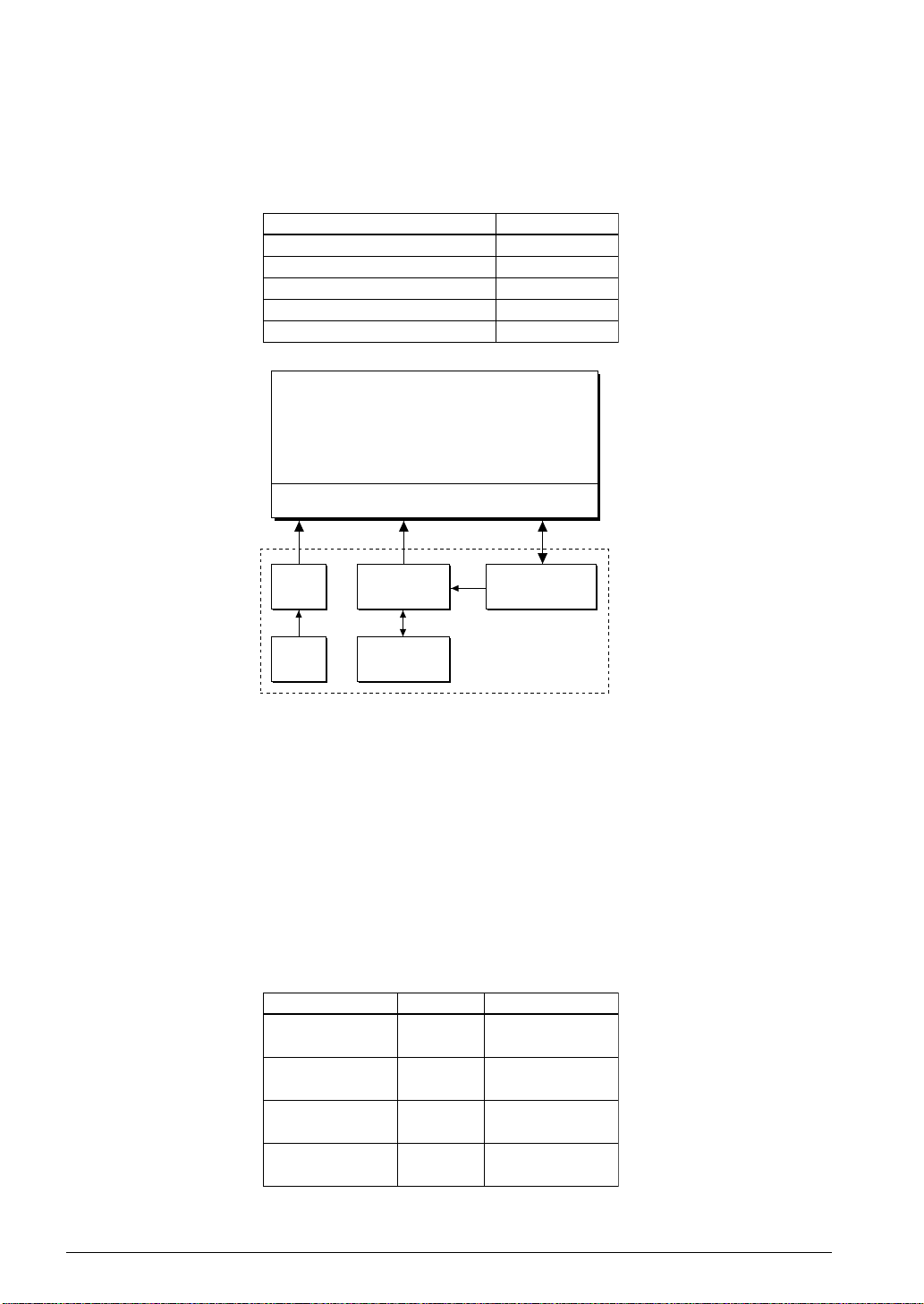
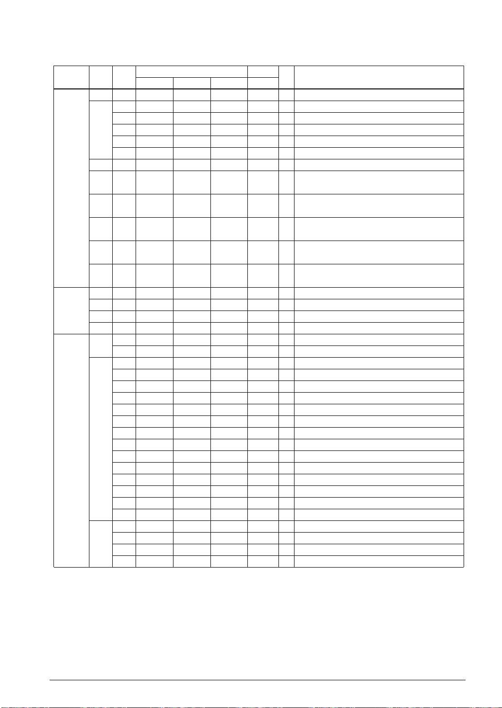
1 DESCRIPTION
1DESCRIPTION
The S1C6200/6200A is the Core CPU of the S1C62 Family of CMOS 4-bit single-chip microcomputers. The CPU features a highly-integrated architecture. Memory-mapped peripheral circuits can include
RAM, ROM, I/O ports, interrupt controllers, timers and LCD drivers, depending upon the application.
The memory address space is divided into program and data memory, each with data and address lines.
Program memory consists of on-chip ROM, containing instructions to be executed by the CPU. Data
memory consists of RAM and memory-mapped I/O, as determined by the design of the peripheral circuitry.
A large memory as well as instructions capable of 8-bit data manipulation enhance the functionality of the
S1C62 Family. Implementation of a common Core CPU ensures that a wide range of application-specific
devices can be designed and fabricated with the minimum turnaround time.
1.1 System Features
• Common Core CPU for all S1C62 Family microcomputers
• UP to 8,192 12-bit words of program memory (ROM)
• UP to 4,096 4-bit words of data memory (RAM/peripheral circuits)
• Memory-mapped I/O
• 5, 7 or 12 clock cycle instructions
• 109 instructions
• Up to 85 levels of subroutine nesting
• 8-bit stack pointer
• Up to 15 interrupt vectors
• Two standby modes
• Low-power CMOS process
1.2 Instruction Set Features
• Four addressing modes: one direct, two indirect, and one stack pointer
• Direct addressing transfers data to and from data memory with a single instruction, resulting in more
efficient code
• 8-bit load instructions and table look-up instructions
• Arithmetic operations in either hexadecimal or decimal
• Arithmetic and logical instructions: addition, subtraction, logical AND, OR, exclusive-OR, comparison
and rotation
1.3 Differences between S1C6200 and S1C6200A
There are some differences in the following operation/circuit between the S1C6200 and the S1C6200A.
For the detailes of each difference, refer to the section enclosed with parentheses.
• Initial setting of D (decimal) flag (refer to Section 2.5.5, "Initial reset".)
• Interrupt circuit
– Interrupt timing (refer to Section 2.5.3, "Operation during interrupt generation".)
– Writing to interrupt mask registers and reading of interrupt flags (refer to Appendix A, "S1C6200A
(Advanced S1C6200) Core CPU".)
S1C6200/6200A CORE CPU MANUAL EPSON 1
Page 8
1 DESCRIPTION
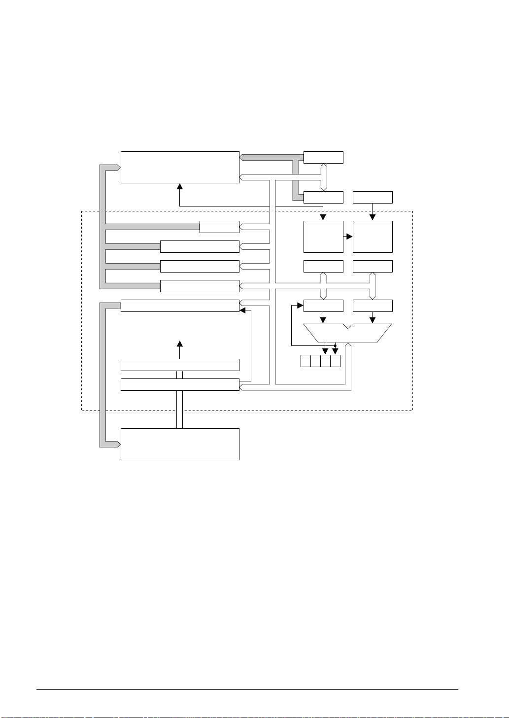
RAM, Peripheral I/O
(4,096 4-bit words max.)
8-bit address bus13-bit address bus
Program Counter Block
Micro-Instructions
Instruction Decorder
Instruction Register (12)
Program Memory
(8,192 12-bit words max.)
Data Memory
YHL (8)
XHL (8)
Stack Pointer (8)
12-bit data bus
ROM
RP (4)
4-bit address bus
4-bit data bus
XP (4)
YP (4)
Interrupt
Controller
A (4)
TEMPB (5)
I DZC
Oscillator
Timing
Generator
B (4)
TEMPA (5)
ALU
S1C6200 CORE CPU
Fig. 1.1 Block diagram
2 EPSON S1C6200/6200A CORE CPU MANUAL
Page 9
2 MEMORY AND OPERATIONS
;
;
;
;
;
;
;
;
;
;
;
;
;
;
;
;
;
;
;
;
;
;
;
;
;
;
;
;
;
;
;
;
;
;
;
;
;
;
;
;
;
;
;
;
;
;
;
;
;
;
;
;
;
;
;
;
;
;
;
;
;;;;;;
;
;
;
;
;
;
;
;
;
;
;
;
;
;
;
;
;
;
;
;
;
;
;
;
;
;
;
;
;
;
;
;
;
;
;
;
;
;;;;;;
;
;
;
;
;
;
;
;
;
;
;
;
;
;
;
;
;
;
;
;
;
;
;
;
;
;
;
;
;
;
;
;
;
;
;
;
;
;
;
;
;
;
;
;
;
;
;
;
;
;
;
;
;
;
;
;;;
2MEMORY AND OPERATIONS
A single-chip microcomputer using the S1C6200/6200A Core CPU has four major blocks: the
program memory (ROM), the data memory (RAM and I/O), the arithmetic logic unit (ALU) and the timing
generator circuit. This section describes each of these blocks in detail.
2.1 Program Memory (ROM)
Program memory contains the instructions that the CPU executes. Figure 2.1.1 shows the configuration of
the program memory.
Each instruction is a 12-bit word. Program memory can also be used for data tables for the table look-up
instructions.
There are two banks of program memory. Each bank is subdivided into 16 pages of 256 words (or steps).
That is:
Program memory = 2 banks
= 8,192 steps
1 bank = 4,096 steps
= 16 pages
1 page = 256 steps
1 step = 1 word
= 12 bits
Certain addresses in ROM have specific functions, as shown in Table 2.1.1.
Table 2.1.1 Allocated program memory
Address Function
Bank 0, Page 1, Step 0
Bank 0, Page 1, Step 1 to 15
Bank 0, Page 0, Step 0 to 255
Bank 1, Page 1, Step 1 to 15
Bank 1, Page 0, Step 0 to 255
Reset vector
Interrupt vectors used while a program is running in bank 0
Bank 0, page 0 area
Direct call subroutines for use by CALZ while a program is running in bank 0
Interrupt vectors used while a program is running in bank 1
Bank 1, page 0 area
Direct call subroutines for use by CALZ while a program is running in bank 1
Page 1
Bank 0
Step 0
Step 1
Step 15
Step 254
Step 255
12-bit
instructions
Reset vector
Interrupt
vectors
for Bank 0
;;;;
;;;;
;;;;
;;;;
;;;;
;;;;
Bank 0
Step 0
Step 1
Step 254
Step 255
Page 0
;;;;;
;;;;;
;;;;;
;;;;;
;;;;;
;;;;;
;;;;;
;;;;;
;;;;;
;;;;;
;;;;;
;;;;;
;;;;;
Bank 0 Bank 1
Bank 0
Step 0
Step 1
Page 3
Bank 0
Page 2
Bank 0
Step 0
;;;;;
;;;;;
;;;;;
;;;;;
;;;;;
;;;;;
;;;;;
;;;;;
;;;;;
;;;;;
;;;;;
;;;;;
;;;;;
;;;;;
;;;;;
;;;;;
;;;;;
;;;;;
;;;;;
;;;;;
;;;;;
;;;;;
;;;;;
;;;;;
Step 254
Step 255
PCB (between banks)
;;
;;
S1C6200/6200A CORE CPU MANUAL EPSON 3
Fig. 2.1.1 Program memory configuration
Page 15
Bank 0
Page 14
;;;;;
;;;;;
;;;;;
;;;;;
;;;;;
;;;;;
;;;;;
;;;;;
;;;;;
;;;;;
;;;;;
;;;;;
;;;;;
;;;;;
;;;;;
;;;;;
;;;;;
;;;;;
;;;;;
;;;;;
;;;;;
;;;;;
;;;;;
;;;;;
PCP
(within bank)
Program or data
code area
PCS
(within bank)
Bank 1
Step 0
Step 1
Step 254
Step 255
;;
;;
Bank 1
Step 0
Page 0
;;;;;
;;;;;
;;;;;
;;;;;
;;;;;
;;;;;
;;;;;
;;;;;
;;;;;
;;;;;
;;;;;
;;;;;
;;;;;
;;;;
;;;;
;;;;
;;;;
;;;;
;;;;
;;;;
Bank 1
;;;;
Step 0
;;;;
;;;;
Step 1
;;;;
;;;;
Step 15
;;;;;
;;;;;
;;;;;
;;;;;
;;;;;
;;;;;
;;;;;
;;;;;
;;;;;
;;;;;
;;;;;
;;;;;
Page 3
Bank 1
Page 2
Step 254
Step 255
Program or data
code or CALZ
subloutines in
Bank 0
Page 1
;;;;;
;;;;;
Interrupt
;;;;;
;;;;;
vectors
;;;;;
for Bank 1
;;;;;
;;;;;
;;;;;
;;;;;
;;;;;
;;;;;
;;;;;
;;
;;
Bank 1
Step 0
Step 1
Step 254
Step 255
Program or data
code or CALZ
subloutines in
Bank 1
Bank 1
Page 14
;;;;;
;;;;;
;;;;;
;;;;;
;;;;;
;;;;;
;;;;;
;;;;;
;;;;;
;;;;;
;;;;;
;;;;;
Page 15
;;;;
;;;;
;;;;
;;;;
;;;;
;;;;
;;;;
;;;;
;;;;
;;;;
;;;;
;;;;
Page 10
2 MEMORY AND OPERATIONS
2.1.1 Program counter block
The program counter is used to point to the next instruction step to be executed by the CPU. See Figure
2.1.1.1.
The program counter has the following registers.
Table 2.1.1.1 Program counter registers
Register Size
PCB (Program Counter-Bank)
PCP (Program Counter-Page)
PCS (Program Counter-Step)
NBP (New Bank Pointer)
NPP (New Page Pointer)
Program memory
(8,192 12-bit words max.)
Address decoder
1-bit register
4-bit counter
8-bit counter
1-bit register
4-bit register
PCB
(1)
NBP
(1)
PCP
(4)
NPP
(4)
PCS
(8)
Program counter block
Fig. 2.1.1.1 Program counter configuration
PCB, PCP and PCS together from a 13-bit counter which can address any location in program memory.
PCP and PCS together from a 12-bit counter which can address any location within a given bank of pro-
gram memory. Each time an instruction other than a jump is executed, this counter increments by one.
Thus, a jump instruction does not need to be executed between the last step of one page and the first step of
the next.
The contents of NBP and NPP are loaded into PCB and PCP each time an instruction is executed. On reset,
NBP and NPP are loaded with the same values as PCB and PCP.
2.1.2 Flags
The following flags are provided.
Table 2.1.2.1 Flags
Flag Size
Interrupt
Decimal mode
Zero
Carry
Menus
I
D
Z
C
1: Enabled
0: Disabled
1: Decimal
0: Hexadecimal
1: Set
0: Ignored
1: Set
0: Ignored
4 EPSON S1C6200/6200A CORE CPU MANUAL
Page 11
2 MEMORY AND OPERATIONS
2.1.3 Jump instructions
A jump can be made using the instructions in Table 2.1.3.1.
Table 2.1.3.1 Jump instructions
Type of jump Instruction
Unconditional
Conditional
Subroutine call
Return
Page set
Indirect
JP
JP C, JP NC, JP Z, JP NZ
CALL, CALZ
RET, RETS, RETD
PSET
JPBA
The differences between jumps within the same page and jumps from one page to another is as follows.
• Jumps within the same page
A jump can be made within the same page using any of the following instructions:
JP, JP C, JP Z, JP NZ, JPBA or CALL
The destination address is specified by the 8-bit operand. A label can be used to specify a destination
address with the S1C62 Family cross assembler.
• Jumps from one page to another
The destination bank and page should be set using PSET before executing a JP instruction.
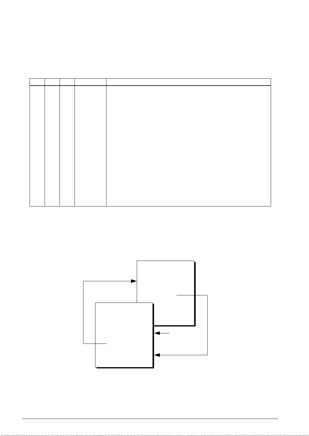
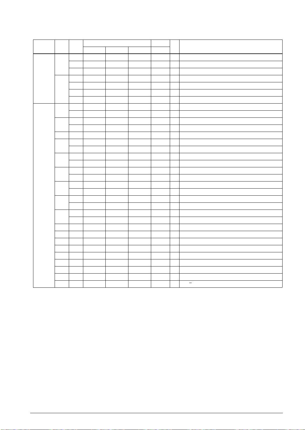
2.1.4 PSET with jump instructions
PSET loads the four low-order bits (page part) of its 5-bit operand to NPP (new page pointer) and loads the
high-order bit (bank part) to NBP (new bank pointer). Executing a JP instruction immediately after PSET
causes a jump to the bank specified by NBP, the page specified by NPP and the step specified by the JP
instruction operand. See Figure 2.1.4.1.
Page 14
PSET
JUMP
Step 0
Step 1
Page 15Bank 0
Jump with PSET can go anywhere
within the program memory
Jump can go between banks
Bank 1
Page 3Bank 1
Page 2Bank 1
Page 1Bank 1
Page 0Bank 1
Bank 1
Step 0
Step 1
Step 254
Step 255
Page 15Bank 1
Page 14
JUMP
Jump without PSET
can go anywhere
Step 0
Step 1
Step 254
Step 255
Bank 0
Page 3Bank 0
Page 2Bank 0
Page 1Bank 0
Page 0Bank 0
Bank 0
Step 0
Step 1
Step 254
Step 255
within one page
Step 254
Step 255
Fig. 2.1.4.1 The PSET and jump instructions
2.1.5 Call instructions
As only the page data specified by NPP is loaded to PCP when a call instruction is executed, subroutine
calls between banks are not possible. Jumps between banks can only be made using JP instructions.
S1C6200/6200A CORE CPU MANUAL EPSON 5
Page 12
2 MEMORY AND OPERATIONS
2.1.6 PSET instruction
Jump or call instructions must follow PSET immediately in order for PSET to affect the destination address.
When a jump or call is not immediately preceded by PSET, the destination address is within the current
page.
Some examples using PSET are shown in Table 2.1.6.1.
Table 2.1.6.1 PSET examples
Bank Page Stap Instruction
PSET
JP
PSET
NOP5
JP
SCF
PSET
JP
RFC
PSET
JP
JP
13H
08H
•
•
15H
09H
•
•
14H
C, 07H
•
•
05H
C, 08H
09H
•
•
0
01H
10H
0
01H
11H
•
•
•
•
•
•
0
01H
21H
0
01H
22H
0
01H
23H
•
•
•
•
•
•
0
01H
55H
0
01H
56H
0
01H
57H
•
•
•
•
•
•
0
01H
60H
0
01H
61H
0
01H
62H
0
01H
63H
•
•
•
•
•
•
The program jumps to bank 1, page 3, step 8.
The data set by PSET is canceled.
The program jumps to bank 0, page 1, step 9.
C flag is set.
The program jumps to bank 1, page 4, step 7 because C flag = 1.
C flag is reset.
No jump occurs because C flag = 0.
The data set by PSET is canceled, and the program jumps to bank 0, page 1, step 9.
Operation
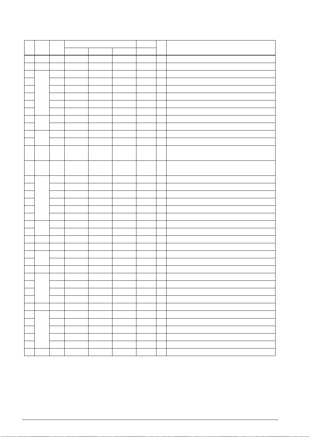
2.1.7 CALZ instruction
CALZ is a direct subroutine call instruction. It calls a subroutine, in page 0 of the current bank, from any
page without requiring the use of PSET.
If CALZ is executed immediately after PSET, the bank and page set by PSET is canceled. This allows direct
subroutine calls to page 0, minimizing repeated code and unnecessary use of PSET. See Figure 2.1.7.1.
Bank 0 Page 0
EEE....................
RET
Bank 0 Page 2
PSET
CALZ
LD
0AH
EEE
A,0
Fig. 2.1.7.1 The use of the CALZ instruction
Not effect
on destination
of CALZ
6 EPSON S1C6200/6200A CORE CPU MANUAL
Page 13
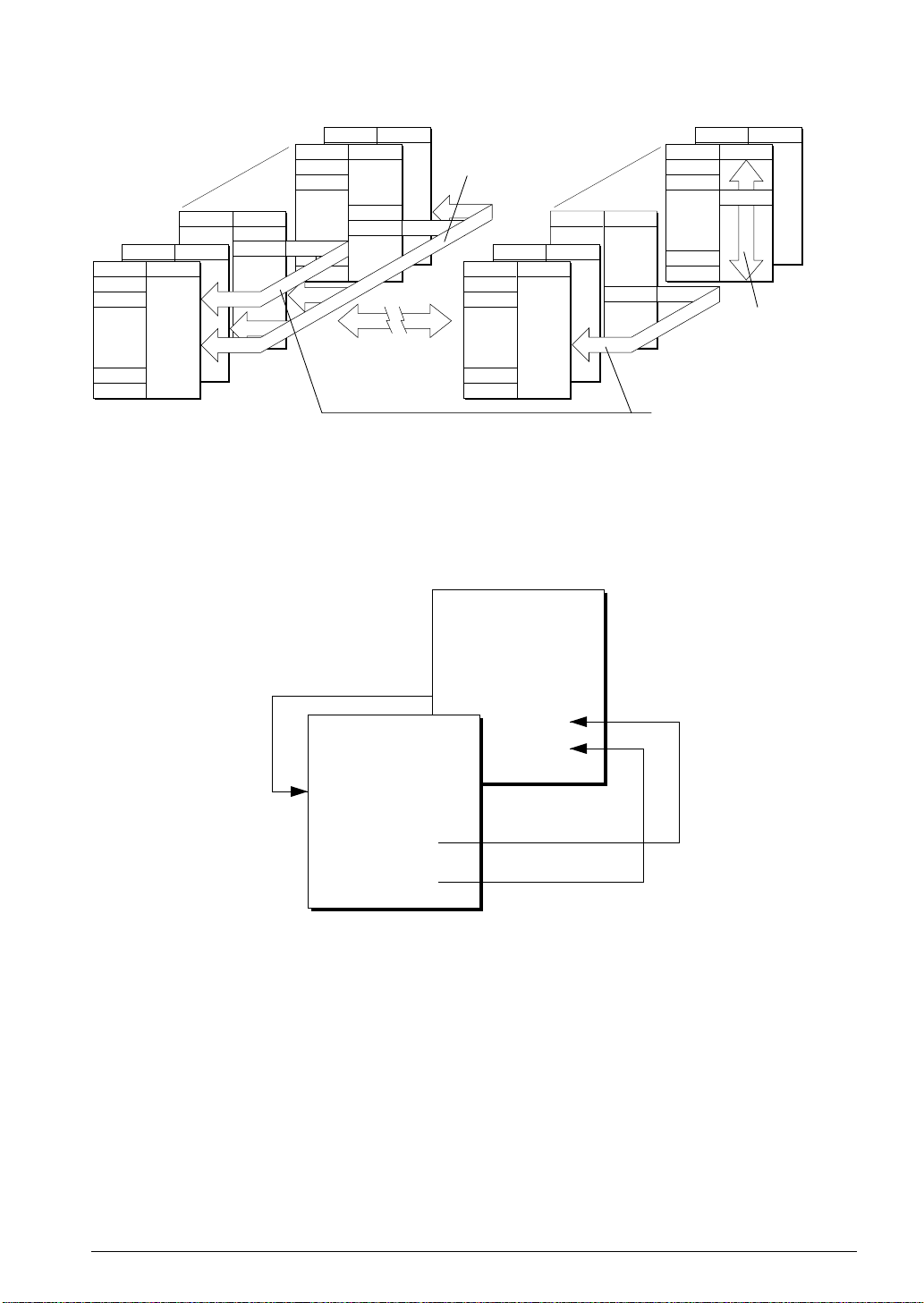
The difference between CALL and CALZ is shown in Figure 2.1.7.2.
2 MEMORY AND OPERATIONS
CALL with PSET
can go anywhere
within a bank
Bank 1
Page 1Bank 1
Page 0Bank 1
Step 0
Step 1
Page 3
CALZ
Bank 1
Step 0
Step 1
Step 254
Step 255
Page 15Bank 1
Page 14
CALL
Step 0
Step 1
Bank 0 Bank 1
Bank 0
Page 3
Page 1Bank 0
Page 0Bank 0
CALZ
Bank 0
Step 0
Step 1
Step 254
Step 255
Page 15Bank 0
Page 14
PSET
CALL
CALL without PSET
can go anywhere
in a page
Step 254
Step 255
CALL and CALZ
cannot go
between banks
Step 254
Step 255
CALZ can only go to page 0
of the current bank
Fig. 2.1.7.2 The difference between CALL and CALZ instructions
2.1.8 RET and RETS instructions
The RET instruction causes a return from a subroutine to the address immediately following the address
from where that subroutine was called. The RETS instruction causes a return to the address following this
address. Proper use of RET and RETS allows simple conditional exits subroutines back to the main routine.
See Figure 2.1.8.1.
Bank 0 Page 0
Program memory
PSET
0AH
CALL
DDD
LD
Bank 0 Page 10
Program memory
LD
A,0
B,0
DDD....................
RET
RETS
Fig. 2.1.8.1 Difference between RET and RETS instructions
2.1.9 Stack considerations for call instructions
When a subroutine is called, the return address is loaded into the stack and retrieved when control is
returned to the calling program. Nesting allows efficient usage of the stack area.
As the stack area resides in the data memory, care should be taken to ensure that the stack area is not
corrupted by other data.
S1C6200/6200A CORE CPU MANUAL EPSON 7
Page 14
2 MEMORY AND OPERATIONS
;
;
;
;
;
;
;
;
;
;
;
;
;
;
;
;
;
;
;
;
;
;
;
;
;
;
;
;
;
;
;
;
;
;
;
;
;
;
;
;
;
;
;
;
;
;
;
;
;
;
;
;
;
;
;
;
;
;
;
;
;
;
;
;
;
;
;
;
;
;
;
;
;
;
;
;
;
;
;
;
;
;
;
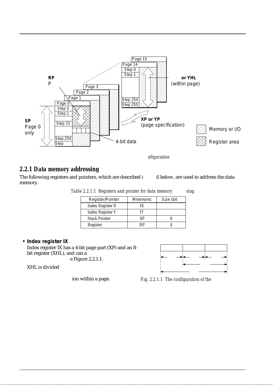
2.2 Data Memory
The data memory area comprises 4,096 4-bit words. The RAM, timer, I/O and other peripheral circuits are
mapped into this memory according to the designer's specifications. Figure 2.2.1 shows the data memory
configuration.
Page 15
SP
Page 0
only
RP
Page 0
only
Page 0
Step 0
Step 1
Step 15
Step 254
Step 255
Page 2
Page 1
;;;;;
;;;;;
;;;;;
;;;;;
;;;;;
;;;;;
;;;;;
;;;;;
;;;;;
;;;;;
;;;;;
;;;;;
;;;;;
;;;;;
;;;;;
;;;;;
;;;;;
;;;;;
;;;;;
Page 14
Step 0
Step 1
Page 3
;;;;;
;;;;;
;;;;;
;;;;;
;;;;;
;;;;;
;;;;;
;;;;;
;;;;;
;;;;;
;;;;;
;;;;;
;;;;;
;;;;;
;;;;;
;;;;;
;;;;;
;;;;;
;;;;;
;;;;;
;;;;;
;;;;;
;;;;;
;;;;;
;;;;;
;;;;;
;;;;;
;;;;;
;;;;;
;;;;;
;;;;;
;;;;;
;;;;;
;;;;;
;;;;;
;;;;;
Step 254
Step 255
4-bit data
Fig. 2.2.1 Data memory configuration
;;;;;
;;;;;
;;;;;
;;;;;
;;;;;
;;;;;
;;;;;
;;;;;
;;;;;
;;;;;
;;;;;
;;;;;
;;;;;
;;;;;
;;;;;
;;;;;
;;;;;
;;;;;
;;;;;
;;;;;
;;;;;
;;;;;
;;;;;
;;;;;
XHL or YHL
(within page)
XP or YP
(page specification)
;;
Memory or I/O
;;
;;
Register area
;;
2.2.1 Data memory addressing
The following registers and pointers, which are described in detail below, are used to address the data
memory.
Table 2.2.1.1 Registers and pointer for data memory addressing
Register/Pointer
Index Register X
Index Register Y
Stack Pointer
Register
• Index register IX
Index register IX has a 4-bit page part (XP) and an 8bit register (XHL), and can address any location in
the data memory. See Figure 2.2.1.1.
XHL is divided into two 4-bit groups: the four highorder bits (XH) and the four low-order bits (XL), and
can address any location within a page.
– MX is the data memory location whose address is specified by IX.
– M(X) refers to the contents of the data memory location whose address is specified by IX.
– XHL can be incremented by 1 or 2 using a post-increment instruction (LDPX, ACPX, SCPX, LBPX or
RETD). An overflow occurring in XHL does not affect the flags.
Mnemonic
IX
IY
SP
RP
Size (bits)
12
12
8
4
MSB
4
XP
44
XH XL
XHL
IX
Fig. 2.2.1.1 The configuration of the index register IX
LSB
8 EPSON S1C6200/6200A CORE CPU MANUAL
Page 15
2 MEMORY AND OPERATIONS
Push-down
(SP is decremented)
Pop-up
(SP is incremented)
Operation Instruction
Stack usage
-3
-3
-1
-1
+3
+1
+1
Interrupt
CALL or CALZ
PUSH
DEC SP
RET, RETS or RETD
POP
INC SP
• Index register IY
Index register IY is like the index register IX: it has a
4-bit page part (YP), an 8-bit register (YHL), and can
address any location in the data memory. See Figure
2.2.1.2.
YHL is divided into two 4-bit groups: the four high-
order bits (YH) and the four low-order bits (YL), and
can address any location within a page.
MSB
4
YP
44
YH YL
YHL
IY
Fig. 2.2.1.2 The configuration of the index register IY
– MY is the data memory location whose address is specified by IY.
– M(Y) refers to the contents of the data memory location whose address is specified by IY.
– YHL can be incremented by 1 using a post-increment instruction (LDPY, ACPY or SCPY). An
overflow occurring in YHL does not affect the flags.
LSB
• Stack pointer SP
The stack area resides in the data memory. The 8-bit, push-down/pop-up stack pointer (SP) is used to
address an element within the stack.
Since it is an 8-bit pointer, SP can only address 256
words out of the total 4,096 words of data memory.
When SP is used, the high-order 4 bits (page part) of
the data memory address are 0, giving a stack area of
256 words in the address range 000H to 0FFH.
In systems with a RAM area of less than 256 words,
the entire RAM area can be used as the stack area.
Stack area usage is shown in Table 2.2.1.2.
The PUSH instruction can be used to store registers and flags in the stack in single-word (4-bit) units.
The POP instruction is used to retrieve this data.
When an interrupt occurs or a call instruction is executed, the return address from the program counter
is pushed onto the stack. When a return instruction is executed, the return address is retrieved from the
stack and loaded into the program counter.
On an interrupt, only the program counter is saved on the stack; flag and register data are not saved.
Programs should be designed so that flag and register data are pushed onto the stack by the interrupt
service routines.
Following a system reset, SP should be initialized using the LD SPH,r or LD SPL,r instructions, where
r represents A, B, MX or MY (4 bits).
Stack pointer data can be read using LD r,SPH or LD r,SPL.
Table 2.2.1.2 Stack usage
• Register pointer RP
The register pointer (RP) is a 4-bit register used to address the first 16 words of data memory, or the
register area. Direct addressing can be used to read from, write to, increment or decrement any location
within this area efficiently, using a single instruction.
Programs cannot directly access RP. It uses the
operand of direct addressing instructions. The
instructions that can access the register area of data
memory are:
LD
LD
LD
S1C6200/6200A CORE CPU MANUAL EPSON 9
LD
INC
DEC
A,Mn
B,Mn
Mn,A
Mn,B
Mn
Mn
A ← M(n)
B ← M(n)
M(n) ← A
M(n) ← B
M(n) ← M(n) + 1
M(n) ← M(n)
n: 0 to F
where M(n) is the contents of a data memory
location within the register area.
As the register area can also be indirectly accessed
–
1
using IX, IY or SP, the stack area should not grow
to address 000H to 00FH when RP is used.
Page 16
2 MEMORY AND OPERATIONS
2.3 ALU (Arithmetic Logic Unit) and Registers
Table 2.3.1 shows ALU operations between the 4-bit registers, TEMPA and TEMPB.
Table 2.3.1 ALU register operation
Operation Instruction
Add, without carry
Add, with carry
Subtract, without borrow
Subtract, with borrow
Logical-AND
Logical-OR
Exclusive-OR
Comparison
Flag bit test
Rotate right, with carry
Rotate left, with carry
Invert
The Z (zero) flag is set when the result of ALU operation is
C3210
X 0000 X: Don't care.
The C (carry) flag is set when an add operation causes a carry or when a subtract operation causes a
borrow.
ADD
ADC
SUB
SBC
AND
OR
XOR
CP
FAN
RRC
RLC
NOT
2.3.1 D (decimal) flag and decimal operations
Setting the D (decimal) flag activates the decimal mode, allowing decimal addition and subtraction. Table
2.3.1.1 shows the relations of actual (decimal) results, ALU outputs, and the values of the C and Z flags.
Table 2.3.1.1 Results of hexadecimal and decimal operations
SubtractionAddition
Actual
result
D = 0 : Result of
hexadecimal operation
Z
1
0
0
1
0
2
0
3
0
4
0
5
0
6
0
7
0
8
0
9
0
10
0
11
0
12
0
13
0
14
0
15
1
16
0
17
0
18
0
19
0
20
0
21
0
22
0
23
0
24
0
25
0
26
0
27
0
28
0
29
0
30
0
31
C
0
0
0
0
0
0
0
0
0
0
0
0
0
0
0
0
1
1
1
1
1
1
1
1
1
1
1
1
1
1
1
1
ALU output
0
1
2
3
4
5
6
7
8
9
A
B
C
D
E
F
0
1
2
3
4
5
6
7
8
9
A
B
C
D
E
F
D = 1 : Result of
decimal operation
C
0
0
0
0
0
0
0
0
0
0
1
1
1
1
1
1
1
1
1
1
1
1
1
1
1
1
1
1
1
1
1
1
ALU output
Z
1
0
0
0
0
0
0
0
0
0
1
0
0
0
0
0
0
0
0
0
0
0
0
0
0
0
1
0
0
0
0
0
Actual
result
0
1
2
3
4
5
6
7
8
9
0
1
2
3
4
5
6
7
8
9
A
B
C
D
E
F
0
1
2
3
4
5
-16
-15
-14
-13
-12
-11
-10
D = 0 : Result of
hexadecimal operation
Z
C
1
1
0
1
0
1
0
1
0
1
0
1
0
1
0
-9
-8
-7
-6
-5
-4
-3
-2
-1
0
1
2
3
4
5
6
7
8
9
10
11
12
13
14
15
1
0
1
0
1
0
1
0
1
0
1
0
1
0
1
0
1
1
0
0
0
0
0
0
0
0
0
0
0
0
0
0
0
0
0
0
0
0
0
0
0
0
0
0
0
0
0
0
0
ALU output
0
1
2
3
4
5
6
7
8
9
A
B
C
D
E
F
0
1
2
3
4
5
6
7
8
9
A
B
C
D
E
F
D = 1 : Result of
decimal operation
C
1
1
1
1
1
1
1
1
1
1
1
1
1
1
1
1
0
0
0
0
0
0
0
0
0
0
0
0
0
0
0
0
ALU output
Z
0
0
0
0
0
0
1
0
0
0
0
0
0
0
0
0
1
0
0
0
0
0
0
0
0
0
0
0
0
0
0
0
A
B
C
D
E
F
0
1
2
3
4
5
6
7
8
9
0
1
2
3
4
5
6
7
8
9
A
B
C
D
E
F
10 EPSON S1C6200/6200A CORE CPU MANUAL
Page 17
2 MEMORY AND OPERATIONS
Hexadecimal operations will not always produce the correct result if performed in decimal mode.
Note that:
• An add instruction with carry (for example, ADC XH,i) which uses index registers XH, XL, YH and YL,
does not involve decimal correction even if it is performed in the decimal mode. This is because it uses
an 8-bit field for 4-bit data.
• The results of the compare instruction (CP) is not decimal-corrected, because the carry flag is ignored.
• The result of the register memory increment instruction (INC Mn) and decrement instruction (DEC Mn)
are not decimal-corrected.
2.3.2 A and B registers
The A and B registers are 4-bit general-purpose registers used as accumulators. They transfer data and
perform ALU operations with other registers, data memory and immediate data.
The data in A can be paired with that in B for use as an indirect jump address by the JPBA instruction.
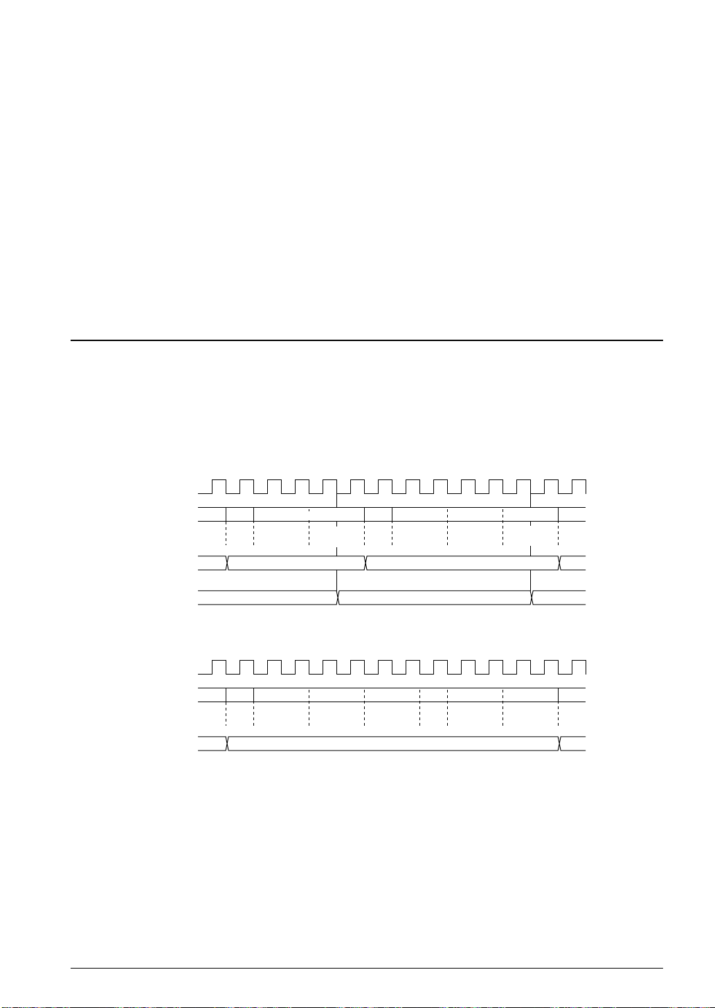
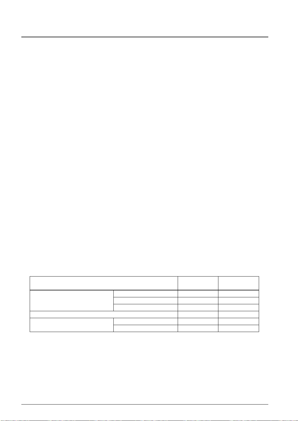
2.4 Timing Generator
S1C6200/6200A instructions can be divided into three different types depending on the number of clock
cycles per instruction: 5, 7 or 12 clock cycles. The more complex the instruction, the more cycles it requires.
Note that the number of clock cycles determines the duration of instructions which, in turn, will affect any
timing performed in software.
As shown in Figure 2.4.1, the first state of all instructions is a fetch cycle. This is followed by a number of
execute cycles.
5-clock/7-clock instructions
Clock
Status
Instruction
register
Date
memory
Fetch ExecuteFetch
State
0
State
1
Execute
State2State0State
1
State
2
State
3
12-clock instructions
Clock
Status
Instruction
register
Fetch
State
0
State
1
State
2
Execute
State3State4State
5
State
6
Fig. 2.4.1 Instruction execution timing
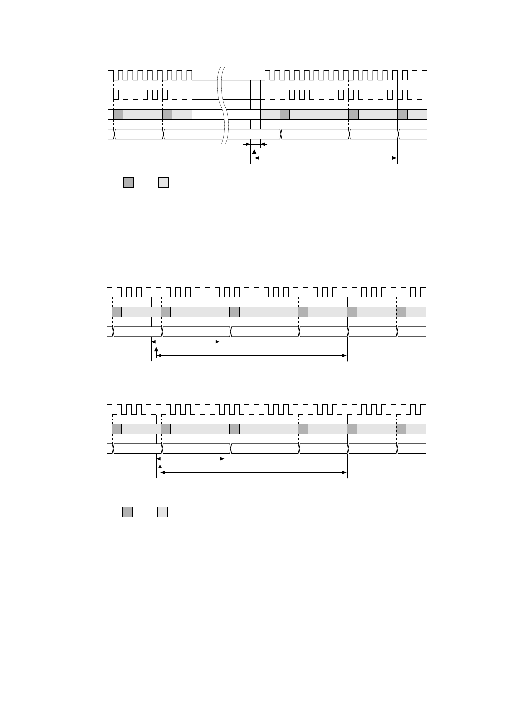
2.4.1 HALT and SLP (sleep) modes
HALT and SLP cause the CPU to store the return address on the stack and then stop. HALT will only stop
the CPU; the system clock will continue to run. SLP also stops the system clock, resulting in reduced power
consumption. The CPU can be restarted by an interrupt.
As interrupts are not automatically enabled by the execution of HALT or SLP, programs should always
enable interrupts before executing HALT or SLP, otherwise they will hang waiting for an interrupt.
S1C6200/6200A CORE CPU MANUAL EPSON 11
Page 18
2 MEMORY AND OPERATIONS
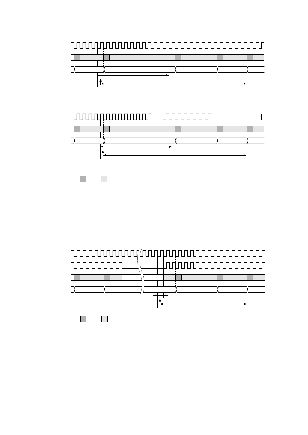
2.5 Interrupts
The S1C6200/6200A can have up to 15 interrupt vectors. When used with peripheral circuits, these allow
internal and external interrupts to be processed easily. See Figure 2.5.3.1 through 2.5.3.4.
2.5.1 Interrupt vectors
The interrupt vectors are assigned to steps 1 to 15 in page 1 of each bank of the program memory. When an
interrupt occurs, the program jumps to the appropriate interrupt vector in the current bank.
The priority and linking of these vectors to actual outside events depends on the configuration of the
peripheral circuits and therefore is device-specific. This information can be found in the technical manuals
for the specific device.
2.5.2 I (interrupt) flag
The I (interrupt) flag enables or disables all interrupts.
When DI or RST F is used to reset the I flag, interrupts are disabled with that instruction step. When EI or
SET F is used to set the I flag, interrupts are enabled after the following instruction step. For example, to
return control from the interrupt subroutine to the main routine, the sequence EI, RET, does not enable
interrupts until after RET has been executed.
The I flag is reset to 0 (DI) on reset.
2.5.3 Operation during interrupt generation
When an interrupt is generated, the program is halted, the program counter (PCP and PCS) is stored on the
stack, the I flag is reset to DI mode and NPP is set to 1. The program then branches to the interrupt vector
corresponding to the interrupt request. Registers and flags are unaffected by an interrupt.
Register and flag data must be saved by the program since they are not automatically stored on the stack.
The I flag can be set to 1 (EI) within the interrupt subroutine, because nesting of multiple interrupts is
available.
If an interrupt is generated while the CPU is in HALT or SLP mode, the CPU is restarted and the interrupt
serviced. When the interrupt service routine is completed, the program resumes from the instruction
following the HALT or SLP.
<Differences between S1C6200 and S1C6200A>
In the S1C6200 and the S1C6200A, the time it takes to complete interrupt processing by hardware after the
Core CPU receives the interrupt request is different as follows:
Table 2.5.3.1 Required interrupt processing time
Item
a) During instruction execution
b) At HALT mode
c) During PSET instruction execution
12 EPSON S1C6200/6200A CORE CPU MANUAL
12-cycle instruction execution
7-cycle instruction execution
5-cycle instruction execution
PSET + CALL
PSET + JP
S1C6200A
(clock cycles)
12.5 to 24.5
12.5 to 19.5
12.5 to 17.5
14 to 15
12.5 to 24.5
12.5 to 22.5
S1C6200
(clock cycles)
13 to 25
13 to 20
13 to 18
14 to 15
13 to 25
13 to 23
Page 19
S1C6200
Clock
Status
2 MEMORY AND OPERATIONS
Instruction
S1C6200A
Clock
Status
Instruction
5-clock Instrruction
5-clock Instrruction
Status:
Fetch
12-clock Instrruction
Interrupt
Interrupt processing:
12-clock Instrruction
Interrupt
Interrupt processing:
Execute Note: (*1)
12-clock instruction
7-clock instruction
5-clock instruction
12-clock instruction
7-clock instruction
5-clock instruction
(*2)
INT1 and INT2 are dummy instructions
Branches to the top of the interrupt service routine
INT1 (*1) INT2 (*1) JP (*2)
... 13 to 25 clock cycles
... 13 to 20 clock cycles
... 13 to 18 clock cycles
INT1 (*1) INT2 (*1) JP (*2)
... 12.5 to 24.5 clock cycles
... 12.5 to 19.5 clock cycles
... 12.5 to 17.5 clock cycles
Fig. 2.5.3.1 Interrupt timing during execution
S1C6200/6200A
System clock
CPU clock
Status
Instruction
Status:
5-clock Instrruction
Fetch
HALT
Execute Note: (*1)
(*2)
Interrupt
Interrupt processing: 14 to 15 clock cycles
INT1 and INT2 are dummy instructions
Branches to the top of the interrupt service routine
INT1 (*1) INT2 (*1) JP (*2)
Fig. 2.5.3.2 Interrupt timing in the HALT mode
S1C6200/6200A CORE CPU MANUAL EPSON 13
Page 20
2 MEMORY AND OPERATIONS
S1C6200/6200A
System clock
CPU clock
Status
Instruction
S1C6200
Clock
Status
Instruction
S1C6200A
Clock
5-clock Instrruction
Status:
PSET
SLEEP
Fetch
Execute Note: (*1)
(*2)
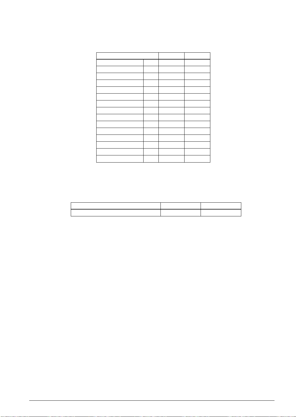
Fig. 2.5.3.3 Interrupt timing in SLEEP mode
CALL
Interrupt
Interrupt processing:
INT1 (*1) INT2 (*1) JP (*2)
PSET + CALL
PSET + JP
INT1 (*1) INT2 (*1) JP (*2)
Interrupt
Interrupt processing: 14 to 15 clock cycles
INT1 and INT2 are dummy instructions
Branches to the top of the interrupt service routine
... 13 to 25 clock cycles
... 13 to 23 clock cycles
Status
Instruction
Status:
PSET
Fetch
CALL
Interrupt
Interrupt processing:
Execute Note: (*1)
PSET + CALL
PSET + JP
INT1 (*1) INT2 (*1) JP (*2)
... 12.5 to 24.5 clock cycles
... 12.5 to 22.5 clock cycles
INT1 and INT2 are dummy instructions
(*2)
Branches to the top of the interrupt service routine
Fig. 2.5.3.4 Interrupt timing with PSET
14 EPSON S1C6200/6200A CORE CPU MANUAL
Page 21
2 MEMORY AND OPERATIONS
2.5.4 Initial reset
On reset, the registers and flags are set as shown in Table 2.5.4.1.
Table 2.5.4.1 Reset value
0
Value
00H
01H
00H
01H
Undefined
Undefined
Undefined
Undefined
Undefined
Undefined
Undefined
0H
*
Undefined
Undefined
* S1C6200 ...Undefined
S1C6200A ...0
S1C6200
Undefined
Bit length
Program Counter Step
Program Counter Page
Program Counter Bank
New Page Pointer
New Bank Pointer
Stack Pointer
Index Register
Index Register
Register Pointer
General Register
General Register
Interrupt Flag
Decimal Flag
Zero Flag
Carry Flag
PCS
PCP
PCB
NPP
NBP
SP
IX
IY
RP
A
B
I
D
Z
C
8
4
1
4
1
8
12
12
4
4
4
1
1
1
1
<Difference between S1C6200 and S1C6200A>
There is a difference in the setting value of the D (decimal) flag at initial reset between the S1C6200 and the
S1C6200A.
Table 2.5.4.2 D (decimal) flag initial setting
CPU Core
D (decimal) flag setting
S1C6200A
When using the model loaded with the S1C6200 Core CPU, set or reset the D flag in the user's initial
routine before using an arithmetic instruction. (refer to the SDF and RDF instructions.)
S1C6200/6200A CORE CPU MANUAL EPSON 15
Page 22

3 INSTRUCTION SET
3INSTRUCTION SET
This chapter describes the entire instruction set of the S1C6200/6200A Core CPU.
A subset is allocated to each device within the S1C62 Family according to the configuration of the device.
Therefore not all instructions are available in every device. The relevant information is in the technical
manual for each device.
The source format and a description of the assembler is in the series-specific cross assembler manuals.
The instruction set contains 109 instructions. Each instruction comprises of one 12-bit word.
3.1 Instruction Indices
Three index tables are used for easy reference instructions.
a. Index by function
The instructions are arranged by function.
1. Branch
2. System control
3. Flag operation
4. Stack operation
5. Index operation
6. Data transfer
7. Arithmetic and logical operation
b. Index in alphabetical order
The instructions are arranged in alphabetical order. Page number references are provided.
c. Index by operation code
The instructions are arranged in numerical order by operation code.
16 EPSON S1C6200/6200A CORE CPU MANUAL
Page 23
3.1.1 By function
3 INSTRUCTION SET
Classification Operand Clock
Branch
instructions
System
control
instructions
Index
operation
instructions
Mne-
monic
PSET
JP
JPBA
CALL
CALZ
RET
RETS
RETD
NOP5
NOP7
HALT
SLP
INC
LD
ADC
p
s
C, s
NC, s
Z, s
NZ, s
s
s
e
X
Y
X, e
Y, e
XP, r
XH, r
XL, r
YP, r
YH, r
YL, r
r, XP
r, XH
r, XL
r, YP
r, YH
r, YL
XH, i
XL, i
YH, i
YL, i
B
1
0
0
0
0
0
1
0
0
1
1
0
1
1
1
1
1
1
1
1
1
1
1
1
1
1
1
1
1
1
1
1
1
1
1
1
Operation Code Flag
A
9
8
7
6
5
4
1
1
0
0
1
0
p4
p3
0
0
0
s7
s6
s5
s4
s3
0
1
0
s7
s6
s5
s4
s3
0
1
1
s7
s6
s5
s4
s3
1
1
0
s7
s6
s5
s4
s3
1
1
1
s7
s6
s5
s4
s3
1
1
1
1
1
1
0
1
0
0
s7
s6
s5
s4
s3
1
0
1
s7
s6
s5
s4
s3
1
1
1
1
1
0
1
1
1
1
1
1
0
1
0
0
1
e7
e6
e5
e4
e3
1
1
1
1
1
1
1
1
1
1
1
1
1
1
1
1
1
1
1
1
1
1
1
1
1
1
1
1
1
1
0
1
1
1
0
1
1
0
1
1
1
1
0
1
1
e7
e6
e5
e4
e3
0
0
0
e7
e6
e5
e4
e3
1
1
0
1
0
0
0
1
1
0
1
0
0
0
1
1
0
1
0
0
0
1
1
0
1
0
0
1
1
1
0
1
0
0
1
1
1
0
1
0
0
1
1
1
0
1
0
1
0
1
1
0
1
0
1
0
1
1
0
1
0
1
0
1
1
0
1
0
1
1
1
1
0
1
0
1
1
1
1
0
1
0
1
1
0
1
0
0
0
0
0
0
1
0
0
0
0
1
0
1
0
0
0
1
0
0
1
0
0
0
1
1
3
2
1
0
IDZC
p2
p1
p0
s2
s1
s0
s2
s1
s0
s2
s1
s0
s2
s1
s0
s2
s1
s0
1
0
0
0
s2
s1
s0
s2
s1
s0
1
1
1
1
1
1
1
0
e2
e1
e0
1
0
1
1
1
1
1
1
1
0
0
0
1
0
0
1
0
0
0
0
0
0
0
0
e2
e1
e0
e2
e1
e0
0
0
r1
r0
0
1
r1
r0
1
0
r1
r0
0
0
r1
r0
0
1
r1
r0
1
0
r1
r0
0
0
r1
r0
0
1
r1
r0
1
0
r1
r0
0
0
r1
r0
0
1
r1
r0
1
0
r1
r0
i3
i2
i1
i0
i3
i2
i1
i0
i3
i2
i1
i0
i3
i2
i1
i0
5
5
5
5
5
5
5
7
7
7
12
12
5
7
5
5
5
5
5
5
5
5
5
5
5
5
5
5
5
5
5
5
↑
↑
7
↓
↓
↑
↑
7
↓
↓
↑
↑
7
↓
↓
↑
↑
7
↓
↓
Operation
←
p4, NPP ← p3~p0
NBP
←
NBP, PCP ← NPP, PCS ← s7~s0
PCB
←
NBP, PCP ← NPP, PCS ← s7~s0 if C=1
PCB
←
NBP, PCP ← NPP, PCS ← s7~s0 if C=0
PCB
←
NBP, PCP ← NPP, PCS ← s7~s0 if Z=1
PCB
←
NBP, PCP ← NPP, PCS ← s7~s0 if Z=0
PCB
←
NBP, PCP ← NPP, PCSH ← B, PCSL ← A
PCB
←
M(SP-1)
SP
M(SP-1)
SP
PCSL
SP
PCSL
SP
PCSL
SP
PCP, M(SP-2) ← PCSH, M(SP-3) ← PCSL+1
←
SP-3, PCP ← NPP, PCS ← s7~s0
←
PCP, M(SP-2) ← PCSH, M(SP-3) ← PCSL+1
←
SP-3, PCP ← 0, PCS ← s7~s0
←
M(SP), PCSH ← M(SP+1), PCP ← M(SP+2)
←
SP+3
←
M(SP), PCSH ← M(SP+1), PCP ← M(SP+2)
←
SP+3, PC ← PC+1
←
M(SP), PCSH ← M(SP+1), PCP ← M(SP+2)
←
SP+3, M(X) ← e3~e0, M(X+1) ← e7~e4, X ← X+2
No operation (5 clock cycles)
No operation (7 clock cycles)
Halt (stop clock)
SLEEP (stop oscillation)
←
X+1
X
←
Y+1
Y
←
e7~e4, XL ← e3~e0
XH
←
e7~e4, YL ← e3~e0
YH
←
r
XP
←
r
XH
←
r
XL
←
r
YP
←
r
YH
←
r
YL
←
XP
r
←
XH
r
←
XL
r
←
YP
r
← Y
H
r
←
YL
r
←
XH+i3~i0+C
XH
←
XL+i3~i0+C
XL
←
YH+i3~i0+C
YH
←
YL+i3~i0+C
YL
S1C6200/6200A CORE CPU MANUAL EPSON 17
Page 24
3 INSTRUCTION SET
Classification Operand
Index
operation
instructions
Mne-
monic
CP
XH, i
XL, i
YH, i
YL, i
Data
transfer
instructions
LD
r, i
r, q
A, Mn
B, Mn
Mn, A
Mn, B
MX, i
LDPX
r, q
MY, i
LDPY
r, q
MX, e
LBPX
Flag
operation
instructions
SET
RST
SCF
F, i
F, i
RCF
SZF
RZF
SDF
RDF
EI
DI
Stack
operation
instructions
INC
DEC
PUSH
SP
SP
r
XP
XH
XL
YP
YH
YL
F
r
POP
XP
XH
XL
YP
Operation Code Flag
B
A
9
8
7
6
5
4
3
2
1
0
IDZC
1
0
1
0
0
1
0
0
i3
i2
i1
i0
1
0
1
0
0
1
0
1
i3
i2
i1
i0
1
0
1
0
0
1
1
0
i3
i2
i1
i0
1
0
1
0
0
1
1
1
i3
i2
i1
i0
1
1
1
0
0
0
r1
r0
i3
i2
i1
i0
1
1
1
0
1
1
0
0
r1
r0
q1
q0
1
1
1
1
1
0
1
0
n3
n2
n1
n0
1
1
1
1
1
0
1
1
n3
n2
n1
n0
1
1
1
1
1
0
0
0
n3
n2
n1
n0
1
1
1
1
1
0
0
1
n3
n2
n1
n0
1
1
1
0
0
1
1
0
i3
i2
i1
i0
1
1
1
0
1
1
1
0
r1
r0
q1
q0
1
1
1
0
0
1
1
1
i3
i2
i1
i0
1
1
1
0
1
1
1
1
r1
r0
q1
q0
1
0
0
1
e7
e6
e5
e4
e3
e2
e1
e0
1
1
1
1
0
1
0
0
i3
1
1
1
1
0
1
0
1
i3
1
1
1
1
0
1
0
0
0
1
1
1
1
0
1
0
1
1
1
1
1
1
0
1
0
0
0
1
1
1
1
0
1
0
1
1
1
1
1
1
0
1
0
0
0
1
1
1
1
0
1
0
1
1
1
1
1
1
0
1
0
0
1
1
1
1
1
0
1
0
1
0
1
1
1
1
1
1
0
1
1
1
1
1
1
1
1
0
0
1
1
1
1
1
1
1
0
0
0
1
1
1
1
1
1
0
0
0
1
1
1
1
1
1
0
0
0
1
1
1
1
1
1
0
0
0
1
1
1
1
1
1
0
0
0
1
1
1
1
1
1
0
0
1
1
1
1
1
1
1
0
0
1
1
1
1
1
1
1
0
0
1
1
1
1
1
1
1
0
1
0
1
1
1
1
1
1
0
1
0
1
1
1
1
1
1
0
1
0
1
1
1
1
1
1
0
1
0
1
1
1
1
1
1
0
1
0
↑
i2
i1
i0
↓
i2
i1
i0
0
0
1
1
1
0
0
1
0
1
0
1
1
0
0
0
1
1
↑
0
0
0
↓
1
1
1
0
1
1
0
1
1
0
r1
r0
1
0
0
1
0
1
1
1
0
1
1
1
0
0
0
0
0
1
0
1
0
0
r1
r0
1
0
0
1
0
1
1
1
0
1
1
1
Clock
↑
↓
↑
↓
↑
↓
↑
↓
↑
↑
↓
↓
↑
↓
↑
↓
XH-i3~i0
↑
7
↓
XL-i3~i0
↑
7
↓
YH-i3~i0
↑
7
↓
YL-i3~i0
↑
7
↓
←
i3~i0
r
5
←
q
r
5
←
M(n3~n0)
A
5
←
M(n3~n0)
B
5
←
M(n3~n0)
5
←
M(n3~n0)
5
←
i3~i0, X ← X+1
M(X)
5
←
q, X ← X+1
r
5
←
i3~i0, Y ← Y+1
M(Y)
5
←
q, Y ← Y+1
r
5
←
e3~e0, M(X+1) ← e7~e4, X ← X+2
M(X)
5
←
FVi3~i0
F
↑
7
←
FΛi3~i0
F
↓
7
←
1
C
↑
7
←
0
C
↓
7
←
1
Z
7
←
0
Z
7
←
1 (Decimal Adjuster ON)
D
7
←
0 (Decimal Adjuster OFF)
D
7
←
1 (Enables Interrupt)
I
7
←
0 (Disables Interrupt)
I
7
←
SP+1
SP
5
←
SP-1
SP
5
←
SP-1, M(SP) ← r
SP
5
←
SP-1, M(SP) ← XP
SP
5
←
SP-1, M(SP) ← XH
SP
5
←
SP-1, M(SP) ← XL
SP
5
←
SP-1, M(SP) ← YP
SP
5
←
SP-1, M(SP) ← YH
SP
5
←
SP-1, M(SP) ← YL
SP
5
←
SP-1, M(SP) ← F
SP
5
←
M(SP), SP ← SP+1
r
5
←
M(SP), SP ← SP+1
XP
5
←
M(SP), SP ← SP+1
XH
5
←
M(SP), SP ← SP+1
XL
5
←
M(SP), SP ← SP+1
YP
5
Operation
A
B
18 EPSON S1C6200/6200A CORE CPU MANUAL
Page 25
3 INSTRUCTION SET
Classification Operand
Stack
operation
instructions
Mne-
monic
POP
LD
YH
YL
F
SPH, r
SPL, r
r, SPH
r, SPL
Arithmetic
instructions
ADD
ADC
r, i
r, q
r, i
r, q
r, q
SUB
r, i
SBC
r, q
r, i
AND
r, q
r, i
OR
r, q
r, i
XOR
r, q
r, i
CP
r, q
r, i
FAN
r, q
r
RLC
r
RRC
Mn
INC
Mn
DEC
MX, r
ACPX
MY, r
ACPY
MX, r
SCPX
MY, r
SCPY
r
NOT
Operation Code Flag
B
A
9
8
7
6
5
4
3
2
1
0
IDZC
1
1
1
1
1
1
0
1
1
0
0
0
1
1
1
1
1
1
0
1
1
0
0
1
1
1
1
1
1
1
0
1
1
0
1
0
↑
1
1
1
1
1
1
1
0
0
0
r1
r0
1
1
1
1
1
1
1
1
0
0
r1
r0
1
1
1
1
1
1
1
0
0
1
r1
r0
1
1
1
1
1
1
1
1
0
1
r1
r0
1
1
0
0
0
0
r1
r0
i3
i2
i1
i0
1
0
1
0
1
0
0
0
r1
r0
q1
q0
1
1
0
0
0
1
r1
r0
i3
i2
i1
i0
1
0
1
0
1
0
0
1
r1
r0
q1
q0
1
0
1
0
1
0
1
0
r1
r0
q1
q0
1
1
0
1
0
1
r1
r0
i3
i2
i1
i0
1
0
1
0
1
0
1
1
r1
r0
q1
q0
1
1
0
0
1
0
r1
r0
i3
i2
i1
i0
1
0
1
0
1
1
0
0
r1
r0
q1
q0
1
1
0
0
1
1
r1
r0
i3
i2
i1
i0
1
0
1
0
1
1
0
1
r1
r0
q1
q0
1
1
0
1
0
0
r1
r0
i3
i2
i1
i0
1
0
1
0
1
1
1
0
r1
r0
q1
q0
1
1
0
1
1
1
r1
r0
i3
i2
i1
i0
1
1
1
1
0
0
0
0
r1
r0
q1
q0
1
1
0
1
1
0
r1
r0
i3
i2
i1
i0
1
1
1
1
0
0
0
1
r1
r0
q1
q0
1
0
1
0
1
1
1
1
r1
r0
r1
r0
1
1
1
0
1
0
0
0
1
1
r1
r0
1
1
1
1
0
1
1
0
n3
n2
n1
n0
1
1
1
1
0
1
1
1
n3
n2
n1
n0
1
1
1
1
0
0
1
0
1
0
r1
r0
1
1
1
1
0
0
1
0
1
1
r1
r0
1
1
1
1
0
0
1
1
1
0
r1
r0
1
1
1
1
0
0
1
1
1
1
r1
r0
1
1
0
1
0
0
r1
r0
1
1
1
1
↑↑
↓↓
★
★
★
★
★
★
★
★
★
★
★
Clock
YH ← M(SP), SP ← SP+1
5
←
M(SP), SP ← SP+1
YL
5
←
M(SP), SP ← SP+1
F
↑
5
↓
↓
←
r
SPH
5
←
r
SPL
5
r
←
SPH
5
←
SPL
r
5
←
7
7
7
7
7
7
7
7
7
7
7
7
7
7
7
7
7
7
5
7
7
7
7
7
7
7
r+i3~i0
r
←
r+q
r
←
r+i3~i0+C
r
←
r+q+C
r
←
r-q
r
←
r-i3~i0-C
r
←
r-q-C
r
←
rΛi3~i0
r
←
rΛq
r
←
rVi3~i0
r
←
rVq
r
←
r∀i3~i0
r
←
r∀q
r
r-i3~i0
r-q
rΛi3~i0
rΛq
←
d2, d2 ← d1, d1 ← d0, d0 ← C, C ← d3
d3
←
C, d2 ← d3, d1 ← d2, d0 ← d1, C ← d0
d3
M(n3~n0)
M(n3~n0)
M(X)
M(Y)
M(X)
M(Y)
r
←
←
←
M(X)+r+C, X ← X+1
←
M(Y)+r+C, Y ← Y+1
←
M(X)-r-C, X ← X+1
←
M(Y)-r-C, Y ← Y+1
←
r
↑
↑
↓
↓
↑
↑
↓
↓
↑
↑
↓
↓
↑
↑
↓
↓
↑
↑
↓
↓
↑
↑
↓
↓
↑
↑
↓
↓
↑
↓
↑
↓
↑
↓
↑
↓
↑
↓
↑
↓
↑
↑
↓
↓
↑
↑
↓
↓
↑
↓
↑
↓
↑
↑
↓
↓
↑
↑
↓
↓
↑
↑
↓
↓
↑
↑
↓
↓
↑
↑
↓
↓
↑
↑
↓
↓
↑
↑
↓
↓
↑
↑
↓
↓
↑
↓
Operation
M(n3~n0)+1
M(n3~n0)-1
S1C6200/6200A CORE CPU MANUAL EPSON 19
Page 26
3 INSTRUCTION SET
3.1.2 In alphabetical order
Mne-
Page Operand Clock
monic
28
ACPX
28
ACPY
29
ADC
29
30
30
31
31
32
ADD
32
AND
33
33
CALL
34
CALZ
34
CP
35
35
36
36
37
37
DEC
38
38
DI
39
EI
39
FAN
40
40
HALT
41
INC
41
42
42
43
JPBA
43
JP
44
44
45
45
46
LBPX
46
MX, r
MY, r
r, i
r, q
XH, i
XL, i
YH, i
YL, i
r, i
r, q
r, i
r, q
s
s
r, i
r, q
XH, i
XL, i
YH, i
YL, i
Mn
SP
r, i
r, q
Mn
SP
X
Y
C, s
NC, s
NZ, s
s
Z, s
MX, e
B
1
1
1
1
1
1
1
1
1
1
1
1
0
0
1
1
1
1
1
1
1
1
1
1
1
1
1
1
1
1
1
1
0
0
0
0
0
1
Operation Code Flag
A
9
8
7
6
5
4
1
1
1
0
0
1
0
1
1
1
0
0
1
0
1
0
0
0
1
r1
r0
0
1
0
1
0
0
1
0
1
0
0
0
0
0
0
1
0
0
0
0
1
0
1
0
0
0
1
0
0
1
0
0
0
1
1
1
0
0
0
0
r1
r0
0
1
0
1
0
0
0
1
0
0
1
0
r1
r0
0
1
0
1
1
0
0
1
0
0
s7
s6
s5
s4
1
0
1
s7
s6
s5
s4
1
0
1
1
1
r1
r0
1
1
1
0
0
0
0
0
1
0
0
1
0
0
0
1
0
0
1
0
1
0
1
0
0
1
1
0
0
1
0
0
1
1
1
1
1
1
0
1
1
1
1
1
1
1
1
0
0
1
1
1
0
1
0
1
1
1
1
0
1
0
0
1
0
1
1
0
r1
r0
1
1
1
0
0
0
1
1
1
1
1
1
1
1
1
1
1
0
1
1
0
1
1
1
1
1
0
1
1
1
0
1
1
1
0
1
1
0
1
1
1
1
1
1
1
1
1
1
0
0
1
0
s7
s6
s5
s4
0
1
1
s7
s6
s5
s4
1
1
1
s7
s6
s5
s4
0
0
0
s7
s6
s5
s4
1
1
0
s7
s6
s5
s4
0
0
1
e7
e6
e5
e4
3
2
1
0
IDZC
1
0
r1
r0
↑
↑
★
1
1
r1
r0
★
i3
i2
i1
i0
★
r1
r0
q1
q0
★
i3
i2
i1
i0
i3
i2
i1
i0
i3
i2
i1
i0
i3
i2
i1
i0
i3
i2
i1
i0
★
r1
r0
q1
q0
★
i3
i2
i1
i0
r1
r0
q1
q0
s3
s2
s1
s0
s3
s2
s1
s0
i3
i2
i1
i0
r1
r0
q1
q0
i3
i2
i1
i0
i3
i2
i1
i0
i3
i2
i1
i0
i3
i2
i1
i0
n3
n2
n1
n0
1
0
1
1
0
1
i3
r1
1
n3
1
0
0
1
s3
s3
s3
s3
s3
e3
↓
1
1
1
↑
0
0
0
i2
i1
i0
r0
q1
q0
0
0
0
n2
n1
n0
0
1
1
0
0
0
0
0
0
0
0
0
s2
s1
s0
s2
s1
s0
s2
s1
s0
s2
s1
s0
s2
s1
s0
e2
e1
e0
7
↓
↓
↑
↑
7
↓
↓
↑
↑
7
↓
↓
↑
↑
7
↓
↓
↑
↑
7
↓
↓
↑
↑
7
↓
↓
↑
↑
7
↓
↓
↑
↑
7
↓
↓
↑
↑
7
↓
↓
↑
↑
7
↓
↓
↑
7
↓
↑
7
↓
7
7
↑
↑
7
↓
↓
↑
↑
7
↓
↓
↑
↑
7
↓
↓
↑
↑
7
↓
↓
↑
↑
7
↓
↓
↑
↑
7
↓
↓
↑
↑
7
↓
↓
5
7
7
↑
7
↓
↑
7
↓
5
↑
↑
7
↓
↓
5
5
5
5
5
5
5
5
5
5
Operation
← M(X)+r+C, X ← X+1
M(X)
← M(Y)+r+C, Y ← Y+1
M(Y)
← r+i3~i0+C
r
← r+q+C
r
← XH+i3~i0+C
XH
← XL+i3~i0+C
XL
← YH+i3~i0+C
YH
← YL+i3~i0+C
YL
← r+i3~i0
r
← r+q
r
← rΛi3~i0
r
← rΛq
r
← PCP, M(SP-2) ← PCSH, M(SP-3) ← PCSL+1
M(SP-1)
← SP-3, PCP ← NPP, PCS ← s7~s0
SP
← PCP, M(SP-2) ← PCSH, M(SP-3) ← PCSL+1
M(SP-1)
← SP-3, PCP ← 0, PCS ← s7~s0
SP
r-i3~i0
r-q
XH-i3~i0
XL-i3~i0
YH-i3~i0
YL-i3~i0
M(n3~n0)
SP
I
I
← M(n3~n0)-1
← SP-1
← 0 (Disables Interrupt)
← 1 (Enables Interrupt)
rΛi3~i0
rΛq
Halt (stop clock)
M(n3~n0)
SP
X
Y
PCB
PCB
PCB
PCB
PCB
PCB
M(X)
← M(n3~n0)+1
← SP+1
← X+1
← Y+1
← NBP, PCP ← NPP, PCSH ← B, PCSL ← A
← NBP, PCP ← NPP, PCS ← s7~s0 if C=1
← NBP, PCP ← NPP, PCS ← s7~s0 if C=0
← NBP, PCP ← NPP, PCS ← s7~s0 if Z=0
← NBP, PCP ← NPP, PCS ← s7~s0
← NBP, PCP ← NPP, PCS ← s7~s0 if Z=1
← e3~e0, M(X+1) ← e7~e4, X ← X+2
20 EPSON S1C6200/6200A CORE CPU MANUAL
Page 27

3 INSTRUCTION SET
Mne-
Page Operand Clock
monic
47
LD
47
48
48
51
51
52
52
53
53
54
54
55
55
56
56
57
58
58
57
59
60
60
59
49
LDPX
49
50
LDPY
50
61
NOP5
61
NOP7
62
NOT
62
OR
63
POP
63
64
64
65
65
66
66
67
A, Mn
B, Mn
Mn, A
Mn, B
r, i
r, q
r, SPH
r, SPL
r, XH
r, XL
r, XP
r, YH
r, YL
r, YP
SPH, r
SPL, r
XH, r
XL, r
XP, r
X, e
YH, r
YL, r
YP, r
Y, e
MX, i
r, q
MY, i
r, q
r
r, i
r, q
F
r
XH
XL
XP
YH
YL
YP
B
1
1
1
1
1
1
1
1
1
1
1
1
1
1
1
1
1
1
1
1
1
1
1
1
1
1
1
1
1
1
1
1
1
1
1
1
1
1
1
1
1
Operation Code Flag
A
9
8
7
6
5
4
1
1
1
1
0
1
0
1
1
1
1
0
1
1
1
1
1
1
0
0
0
1
1
1
1
0
0
1
1
1
0
0
0
r1
r0
1
1
0
1
1
0
0
1
1
1
1
1
1
0
1
1
1
1
1
1
1
1
1
0
1
0
1
0
1
1
0
1
0
1
0
1
1
0
1
0
1
0
1
1
0
1
0
1
1
1
1
0
1
0
1
1
1
1
0
1
0
1
1
1
1
1
1
1
1
0
1
1
1
1
1
1
1
1
1
0
1
0
0
0
1
1
0
1
0
0
0
1
1
0
1
0
0
0
0
1
1
e7
e6
e5
e4
1
1
0
1
0
0
1
1
1
0
1
0
0
1
1
1
0
1
0
0
1
0
0
0
e7
e6
e5
e4
1
1
0
0
1
1
0
1
1
0
1
1
1
0
1
1
0
0
1
1
1
1
1
0
1
1
1
1
1
1
1
1
1
1
1
1
1
1
1
1
1
1
1
0
1
0
0
r1
r0
1
0
0
1
1
r1
r0
0
1
0
1
1
0
1
1
1
1
1
1
0
1
1
1
1
1
1
0
1
1
1
1
1
1
0
1
1
1
1
1
1
0
1
1
1
1
1
1
0
1
1
1
1
1
1
0
1
1
1
1
1
1
0
1
1
1
1
1
1
0
1
3
2
1
0
IDZC
n3
n2
n1
n0
n3
n2
n1
n0
n3
n2
n1
n0
n3
n2
n1
n0
i3
i2
i1
i0
r1
r0
q1
q0
0
1
r1
r0
0
1
r1
r0
0
1
r1
r0
1
0
r1
r0
0
0
r1
r0
0
1
r1
r0
1
0
r1
r0
0
0
r1
r0
0
0
r1
r0
0
0
r1
r0
0
1
r1
r0
1
0
r1
r0
0
0
r1
r0
e3
e2
e1
e0
0
1
r1
r0
1
0
r1
r0
0
0
r1
r0
e3
e2
e1
e0
i3
i2
i1
i0
r1
r0
q1
q0
i3
i2
i1
i0
r1
r0
q1
q0
1
0
1
1
1
1
1
1
1
1
1
1
i3
i2
i1
i0
r1
r0
q1
q0
1
0
1
0
↓
0
0
r1
r0
0
1
0
1
0
1
1
0
0
1
0
0
1
0
0
0
1
0
0
1
0
1
1
1
5
5
5
5
5
5
5
5
5
5
5
5
5
5
5
5
5
5
5
5
5
5
5
5
5
5
5
5
5
7
↑
7
↓
↑
7
↓
↑
7
↓
↑
↑↓↑
↑
5
↓
↓
5
5
5
5
5
5
5
Operation
←
M(n3~n0)
A
←
M(n3~n0)
B
←
M(n3~n0)
M(n3~n0)
←
r
←
r
←
r
←
r
←
r
←
r
←
r
←
r
←
r
←
r
SPH
SPL
XH
←
XL
←
XP
XH
YH
←
YL
←
YP
YH
M(X)
←
r
M(Y)
←
r
A
←
B
i3~i0
q
SPH
SPL
XH
XL
XP
YH
YL
YP
←
r
←
r
←
r
r
r
←
e7~e4, XL ← e3~e0
←
r
r
r
←
e7~e4, YL ← e3~e0
←
i3~i0, X ← X+1
q, X ← X+1
←
i3~i0, Y ← Y+1
q, Y ← Y+1
No operation (5 clock cycles)
No operation (7 clock cycles)
←
r
r
←
rVi3~i0
r
←
rVq
r
←
M(SP), SP ← SP+1
F
←
M(SP), SP ← SP+1
r
←
M(SP), SP ← SP+1
XH
←
M(SP), SP ← SP+1
XL
←
M(SP), SP ← SP+1
XP
←
M(SP), SP ← SP+1
YH
←
M(SP), SP ← SP+1
YL
←
M(SP), SP ← SP+1
YP
S1C6200/6200A CORE CPU MANUAL EPSON 21
Page 28
3 INSTRUCTION SET
Mne-
Page Operand Clock
monic
67
PSET
68
PUSH
68
69
69
70
70
71
71
RCF
72
RDF
72
RET
73
RETD
73
RETS
74
RLC
74
RRC
75
RST
75
RZF
76
SBC
76
77
SCF
77
SCPX
78
SCPY
78
SDF
79
SET
79
SLP
80
SUB
80
SZF
81
XOR
81
82
p
F
r
XH
XL
XP
YH
YL
YP
e
r
r
F, i
r, i
r, q
MX, r
MY, r
F, i
r, q
r, i
r, q
B
1
1
1
1
1
1
1
1
1
1
1
1
0
1
1
1
1
1
1
1
1
1
1
1
1
1
1
1
1
1
Operation Code Flag
A
9
8
7
6
5
4
1
1
0
0
1
0
p4
1
1
1
1
1
0
0
1
1
1
1
1
0
0
1
1
1
1
1
0
0
1
1
1
1
1
0
0
1
1
1
1
1
0
0
1
1
1
1
1
0
0
1
1
1
1
1
0
0
1
1
1
1
1
0
0
1
1
1
0
1
0
1
1
1
1
0
1
0
1
1
1
1
1
1
0
1
0
0
1
e7
e6
e5
e4
1
1
1
1
1
0
1
0
1
0
1
1
1
1
1
1
0
1
0
0
0
1
1
1
0
1
0
1
1
1
1
0
1
0
1
1
0
1
0
1
r1
r0
0
1
0
1
0
1
1
1
1
1
0
1
0
0
1
1
1
0
0
1
1
1
1
1
0
0
1
1
1
1
1
0
1
0
0
1
1
1
0
1
0
0
1
1
1
1
1
1
1
0
1
0
1
0
1
0
1
1
1
0
1
0
0
1
0
1
0
0
r1
r0
0
1
0
1
1
1
0
3
2
1
0
IDZC
p3
p2
p1
p0
1
0
1
0
0
0
r1
r0
0
1
0
1
0
1
1
0
0
1
0
0
1
0
0
0
1
0
0
1
0
1
1
1
1
1
1
0
1
0
1
1
1
1
1
1
e3
e2
e1
e0
1
1
1
0
r1
r0
r1
r0
1
1
r1
r0
i3
1
i3
r1
r0
0
1
1
0
i3
1
r1
r0
0
i3
r1
r0
↓
i2
i1
i0
1
0
1
i2
i1
i0
q1
q0
0
0
1
0
r1
r0
1
r1
r0
1
0
0
↑
i2
i1
i0
0
0
1
q1
q0
0
1
0
i2
i1
i0
q1
q0
5
5
5
5
5
5
5
5
5
↓
7
↓
7
7
12
12
↑
↑
7
↓
↓
↑
↑
5
↓
↓
↓
↓
↓
7
↓
7
★
↑
↑
7
↓
↓
★
↑
↑
7
↓
↓
↑
7
★
↑
↑
7
↓
↓
★
↑
↑
7
↓
↓
↑
7
↑
↑
↑
7
5
★
↑
↑
7
↓
↓
↑
7
↑
7
↓
↑
7
↓
Operation
← p4, NPP ← p3~p0
NBP
← SP-1, M(SP) ← F
SP
← SP-1, M(SP) ← r
SP
← SP-1, M(SP) ← XH
SP
← SP-1, M(SP) ← XL
SP
← SP-1, M(SP) ← XP
SP
← SP-1, M(SP) ← YH
SP
← SP-1, M(SP) ← YL
SP
← SP-1, M(SP) ← YP
SP
← 0
C
← 0 (Decimal Adjuster OFF)
D
← M(SP), PCSH ← M(SP+1), PCP ← M(SP+2)
PCSL
← SP+3
SP
← M(SP), PCSH ← M(SP+1), PCP ← M(SP+2)
PCSL
← SP+3, M(X) ← e3~e0, M(X+1) ← e7~e4, X ← X+2
SP
← M(SP), PCSH ← M(SP+1), PCP ← M(SP+2)
PCSL
← SP+3, PC ← PC+1
SP
← d2, d2 ← d1, d1 ← d0, d0 ← C, C ← d3
d3
← C, d2 ← d3, d1 ← d2, d0 ← d1, C ← d0
d3
← FΛi3~i0
F
← 0
Z
← r-i3~i0-C
r
← r-q-C
r
← 1
C
← M(X)-r-C, X ← X+1
M(X)
← M(Y)-r-C, Y ← Y+1
M(Y)
← 1 (Decimal Adjuster ON)
D
← FVi3~i0
F
SLEEP (stop oscillation)
← r-q
r
← 1
Z
← r∀i3~i0
r
← r∀q
r
22 EPSON S1C6200/6200A CORE CPU MANUAL
Page 29
3.1.3 By operation code
3 INSTRUCTION SET
Operation
Code (HEX)
000 to 0FF
100 to 1FF
200 to 2FF
300 to 3FF
400 to 4FF
500 to 5FF
600 to 6FF
700 to 7FF
800 to 8FF
900 to 9FF
A00 to A0F
A10 to A1F
A20 to A2F
A30 to A3F
A40 to A4F
A50 to A5F
A60 to A6F
A70 to A7F
A80 to A8F
A90 to A9F
AA0 to AAF
AB0 to ABF
AC0 to ACF
AD0 to ADF
AE0 to AEF
AF0 to AFF
B00 to BFF
C00 to C3F
C40 to C7F
C80 to CBF
CC0 to CFF
D00 to D3F
D0F to D3F
D40 to D7F
D80 to DBF
DC0 to DFF
E00 to E3F
Mne-
Operand Clock
monic
JP
RETD
JP
JP
CALL
CALZ
JP
JP
LD
LBPX
ADC
ADC
ADC
ADC
CP
CP
CP
CP
ADD
ADC
SUB
SBC
AND
OR
XOR
RLC
LD
ADD
ADC
AND
OR
XOR
NOT
SBC
FAN
CP
LD
s
e
C, s
NC, s
s
s
Z, s
NZ, s
Y, e
MX, e
XH, i
XL, i
YH, i
YL, i
XH, i
XL, i
YH, i
YL, i
r, q
r, q
r, q
r, q
r, q
r, q
r, q
r
X, e
r, i
r, i
r, i
r, i
r, i
r
r, i
r, i
r, i
r, i
B
0
0
0
0
0
0
0
0
1
1
1
1
1
1
1
1
1
1
1
1
1
1
1
1
1
1
1
1
1
1
1
1
1
1
1
1
1
Operation Code Flag
A
9
8
7
6
5
4
0
0
0
s7
s6
s5
s4
0
0
1
e7
e6
e5
e4
0
1
0
s7
s6
s5
s4
0
1
1
s7
s6
s5
s4
1
0
0
s7
s6
s5
s4
1
0
1
s7
s6
s5
s4
1
1
0
s7
s6
s5
s4
1
1
1
s7
s6
s5
s4
0
0
0
e7
e6
e5
e4
0
0
1
e7
e6
e5
e4
0
1
0
0
0
0
0
0
1
0
0
0
0
1
0
1
0
0
0
1
0
0
1
0
0
0
1
1
0
1
0
0
1
0
0
0
1
0
0
1
0
1
0
1
0
0
1
1
0
0
1
0
0
1
1
1
0
1
0
1
0
0
0
0
1
0
1
0
0
1
0
1
0
1
0
1
0
0
1
0
1
0
1
1
0
1
0
1
1
0
0
0
1
0
1
1
0
1
0
1
0
1
1
1
0
0
1
0
1
1
1
1
0
1
1
e7
e6
e5
e4
1
0
0
0
0
r1
r0
1
0
0
0
1
r1
r0
1
0
0
1
0
r1
r0
1
0
0
1
1
r1
r0
1
0
1
0
0
r1
r0
1
0
1
0
0
r1
r0
1
0
1
0
1
r1
r0
1
0
1
1
0
r1
r0
1
0
1
1
1
r1
r0
1
1
0
0
0
r1
r0
3
2
1
0
s3
s2
s1
s0
e3
e2
e1
e0
s3
s2
s1
s0
s3
s2
s1
s0
s3
s2
s1
s0
s3
s2
s1
s0
s3
s2
s1
s0
s3
s2
s1
s0
e3
e2
e1
e0
e3
e2
e1
e0
i3
i2
i1
i0
i3
i2
i1
i0
i3
i2
i1
i0
i3
i2
i1
i0
i3
i2
i1
i0
i3
i2
i1
i0
i3
i2
i1
i0
i3
i2
i1
i0
r1
r0
q1
q0
r1
r0
q1
q0
r1
r0
q1
q0
r1
r0
q1
q0
r1
r0
q1
q0
r1
r0
q1
q0
r1
r0
q1
q0
r1
r0
r1
r0
e3
e2
e1
e0
i3
i2
i1
i0
i3
i2
i1
i0
i3
i2
i1
i0
i3
i2
i1
i0
i3
i2
i1
i0
1
1
1
1
i3
i2
i1
i0
i3
i2
i1
i0
i3
i2
i1
i0
i3
i2
i1
i0
IDZC
↑
↑
↓
↓
↑
↑
↓
↓
↑
↑
↓
↓
↑
↑
↓
↓
↑
↑
↓
↓
↑
↑
↓
↓
↑
↑
↓
↓
↑
↑
↓
↓
★
↑
↑
↓
↓
★
↑
↑
↓
↓
★
↑
↑
↓
↓
★
↑
↑
↓
↓
↑
↓
↑
↓
↑
↓
↑
↑
↓
↓
★
↑
↑
↓
↓
★
↑
↑
↓
↓
↑
↓
↑
↓
↑
↓
↑
↓
★
↑
↑
↓
↓
↑
↓
↑
↑
↓
↓
12
5
5
5
7
7
5
5
5
5
7
7
7
7
7
7
7
7
7
7
7
7
7
7
7
7
5
7
7
7
7
7
7
7
7
7
5
Operation
←
NBP, PCP ← NPP, PCS ← s7~s0
PCB
←
M(SP), PCSH ← M(SP+1), PCP ← M(SP+2)
PCSL
←
SP+3, M(X) ← e3~e0, M(X+1) ← e7~e4, X ← X+2
SP
←
NBP, PCP ← NPP, PCS ← s7~s0 if C=1
PCB
←
NBP, PCP ← NPP, PCS ← s7~s0 if C=0
PCB
←
M(SP-1)
SP
M(SP-1)
SP
PCB
PCB
YH
M(X)
XH
XL
YH
YL
PCP, M(SP-2) ← PCSH, M(SP-3) ← PCSL+1
←
SP-3, PCP ← NPP, PCS ← s7~s0
←
PCP, M(SP-2) ← PCSH, M(SP-3) ← PCSL+1
←
SP-3, PCP ← 0, PCS ← s7~s0
←
NBP, PCP ← NPP, PCS ← s7~s0 if Z=1
←
NBP, PCP ← NPP, PCS ← s7~s0 if Z=0
←
e7~e4, YL ← e3~e0
←
e3~e0, M(X+1) ← e7~e4, X ← X+2
←
XH+i3~i0+C
←
XL+i3~i0+C
←
YH+i3~i0+C
←
YL+i3~i0+C
XH-i3~i0
XL-i3~i0
YH-i3~i0
YL-i3~i0
←
r+q
r
←
r+q+C
r
←
r-q
r
←
r-q-C
r
←
rΛq
r
←
rVq
r
←
r∀q
r
←
d2, d2 ← d1, d1 ← d0, d0 ← C, C ← d3
d3
←
e7~e4, XL ← e3~e0
XH
←
r+i3~i0
r
←
r+i3~i0+C
r
←
rΛi3~i0
r
←
rVi3~i0
r
←
r∀i3~i0
r
←
r
r
←
r-i3~i0-C
r
rΛi3~i0
r-i3~i0
←
i3~i0
r
S1C6200/6200A CORE CPU MANUAL EPSON 23
Page 30
3 INSTRUCTION SET
Operation
Code (HEX)
E40 to E5F
E60 to E6F
E70 to E7F
E80 to E83
E84 to E87
E88 to E8B
E8C to E8F
E90 to E93
E94 to E97
E98 to E9B
EA0 to EA3
EA4 to EA7
EA8 to EAB
EB0 to EB3
EB4 to EB7
EB8 to EBB
EC0 to ECF
EE0
EE0 to EEF
EF0
EF0 to EFF
F00 to F0F
F10 to F1F
F28 to F2B
F2C to F2F
F38 to F3B
F3C to F3F
F40 to F4F
F41
F42
F44
F48
F50 to F5F
F57
F5B
F5D
F5E
F60 to F6F
F70 to F7F
F80 to F8F
Mne-
Operand Clock
monic
PSET
LDPX
LDPY
LD
LD
LD
RRC
LD
LD
LD
LD
LD
LD
LD
LD
LD
LD
INC
LDPX
INC
LDPY
CP
FAN
ACPX
ACPY
SCPX
SCPY
SET
SCF
SZF
SDF
EI
RST
DI
RDF
RZF
RCF
INC
DEC
LD
p
MX, i
MY, i
XP, r
XH, r
XL, r
r
YP, r
YH, r
YL, r
r, XP
r, XH
r, XL
r, YP
r, YH
r, YL
r, q
X
r, q
Y
r, q
r, q
r, q
MX, r
MY, r
MX, r
MY, r
F, i
F, i
Mn
Mn
Mn, A
B
1
1
1
1
1
1
1
1
1
1
1
1
1
1
1
1
1
1
1
1
1
1
1
1
1
1
1
1
1
1
1
1
1
1
1
1
1
1
1
1
Operation Code Flag
A
9
8
7
6
5
4
1
1
0
0
1
0
p4
p3
1
1
0
0
1
1
0
1
1
0
0
1
1
1
1
1
0
1
0
0
0
1
1
0
1
0
0
0
1
1
0
1
0
0
0
1
1
0
1
0
0
0
1
1
0
1
0
0
1
1
1
0
1
0
0
1
1
1
0
1
0
0
1
1
1
0
1
0
1
0
1
1
0
1
0
1
0
1
1
0
1
0
1
0
1
1
0
1
0
1
1
1
1
0
1
0
1
1
1
1
0
1
0
1
1
1
1
0
1
1
0
0
1
1
0
1
1
1
0
1
1
0
1
1
1
0
1
1
0
1
1
1
1
1
1
0
1
1
1
1
1
1
1
0
0
0
0
1
1
1
0
0
0
1
1
1
1
0
0
1
0
1
1
1
0
0
1
0
1
1
1
0
0
1
1
1
1
1
0
0
1
1
1
1
1
0
1
0
0
1
1
1
0
1
0
0
1
1
1
0
1
0
0
1
1
1
0
1
0
0
1
1
1
0
1
0
0
1
1
1
0
1
0
1
1
1
1
0
1
0
1
1
1
1
0
1
0
1
1
1
1
0
1
0
1
1
1
1
0
1
0
1
1
1
1
0
1
1
0
n3
1
1
1
0
1
1
1
n3
1
1
1
1
0
0
0
n3
3
2
1
0
p2
p1
p0
i3
i2
i1
i0
i3
i2
i1
i0
0
0
r1
r0
0
1
r1
r0
1
0
r1
r0
1
1
r1
r0
0
0
r1
r0
0
1
r1
r0
1
0
r1
r0
0
0
r1
r0
0
1
r1
r0
1
0
r1
r0
0
0
r1
r0
0
1
r1
r0
1
0
r1
r0
r1
r0
q1
q0
0
0
0
0
r1
r0
q1
q0
0
0
0
0
r1
r0
q1
q0
r1
r0
q1
q0
r1
r0
q1
q0
1
0
r1
r0
1
1
r1
r0
1
0
r1
r0
1
1
r1
r0
i3
i2
i1
i0
0
0
0
1
0
0
1
0
0
1
0
0
1
0
0
0
i3
i2
i1
i0
0
1
1
1
1
0
1
1
1
1
0
1
1
1
1
0
n2
n1
n0
n2
n1
n0
n2
n1
n0
IDZC
↑
↓
↑
↓
↑
↓
★
↑
↓
★
↑
↓
★
↑
↓
★
↑
↓
↑
↑
↑
↑
↑
↑
↓
↓
↓
↓
↓
↓
↑
↓
↑
↓
Operation
←
5
5
5
5
5
5
↑
5
↓
5
5
5
5
5
5
5
5
5
5
5
5
5
5
↑
7
↓
7
↑
7
↓
↑
7
↓
↑
7
↓
↑
7
↓
↑
7
↑
7
7
7
7
↓
7
7
7
7
↓
7
↑
7
↓
↑
7
↓
5
p4, NPP ← p3~p0
NBP
←
i3~i0, X ← X+1
M(X)
←
i3~i0, Y ← Y+1
M(Y)
←
r
XP
←
r
XH
←
r
XL
←
C, d2 ← d3, d1 ← d2, d0 ← d1, C ← d0
d3
←
r
YP
←
r
YH
←
r
YL
←
XP
r
←
XH
r
←
XL
r
←
YP
r
←
YH
r
←
YL
r
←
q
r
←
X+1
X
←
q, X ← X+1
r
←
Y+1
Y
←
q, Y ← Y+1
r
r-q
rΛq
←
M(X)+r+C, X ← X+1
M(X)
←
M(Y)+r+C, Y ← Y+1
M(Y)
←
M(X)-r-C, X ← X+1
M(X)
←
M(Y)-r-C, Y ← Y+1
M(Y)
←
FVi3~i0
F
←
1
C
←
1
Z
←
1 (Decimal Adjuster ON)
D
←
1 (Enables Interrupt)
I
←
FΛi3~i0
F
←
0 (Disables Interrupt)
I
←
0 (Decimal Adjuster OFF)
D
←
0
Z
←
0
C
←
M(n3~n0)
M(n3~n0)
M(n3~n0)
M(n3~n0)+1
←
M(n3~n0)-1
←
A
24 EPSON S1C6200/6200A CORE CPU MANUAL
Page 31

3 INSTRUCTION SET
Operation
Code (HEX)
F90 to F9F
FA0 to FAF
FB0 to FBF
FC0 to FC3
FC4
FC5
FC6
FC7
FC8
FC9
FCA
FCB
FD0 to FD3
FD4
FD5
FD6
FD7
FD8
FD9
FDA
FDB
FDE
FDF
FE0 to FE3
FE4 to FE7
FE8
FF0 to FF3
FF4 to FF7
FF8
FF9
FFB
FFF
Mne-
Operand Clock
monic
LD
LD
LD
PUSH
PUSH
PUSH
PUSH
PUSH
PUSH
PUSH
PUSH
DEC
POP
POP
POP
POP
POP
POP
POP
POP
INC
RETS
RET
LD
LD
JPBA
LD
LD
HALT
SLP
NOP5
NOP7
Mn, B
A, Mn
B, Mn
r
XP
XH
XL
YP
YH
YL
F
SP
r
XP
XH
XL
YP
YH
YL
F
SP
SPH, r
r, SPH
SPL, r
r, SPL
B
1
1
1
1
1
1
1
1
1
1
1
1
1
1
1
1
1
1
1
1
1
1
1
1
1
1
1
1
1
1
1
1
Operation Code Flag
A
9
8
7
6
5
4
1
1
1
1
0
0
1
1
1
1
1
0
1
0
1
1
1
1
0
1
1
1
1
1
1
1
0
0
1
1
1
1
1
0
0
1
1
1
1
1
0
0
1
1
1
1
1
0
0
1
1
1
1
1
0
0
1
1
1
1
1
0
0
1
1
1
1
1
0
0
1
1
1
1
1
0
0
1
1
1
1
1
0
0
1
1
1
1
1
0
1
1
1
1
1
1
0
1
1
1
1
1
1
0
1
1
1
1
1
1
0
1
1
1
1
1
1
0
1
1
1
1
1
1
0
1
1
1
1
1
1
0
1
1
1
1
1
1
0
1
1
1
1
1
1
0
1
1
1
1
1
1
0
1
1
1
1
1
1
0
1
1
1
1
1
1
1
0
1
1
1
1
1
1
0
1
1
1
1
1
1
0
1
1
1
1
1
1
1
1
1
1
1
1
1
1
1
1
1
1
1
1
1
1
1
1
1
1
1
1
1
1
1
1
1
1
1
1
1
1
1
1
1
1
3
2
1
0
n3
n2
n1
n0
n3
n2
n1
n0
n3
n2
n1
n0
0
0
r1
r0
0
1
0
0
0
1
0
1
0
1
1
0
0
1
1
1
1
0
0
0
1
0
0
1
1
0
1
0
1
0
1
1
0
0
r1
r0
0
1
0
0
0
1
0
1
0
1
1
0
0
1
1
1
1
0
0
0
1
0
0
1
1
0
1
0
1
0
1
1
1
1
1
0
1
1
1
1
0
0
r1
r0
0
1
r1
r0
1
0
0
0
0
0
r1
r0
0
1
r1
r0
1
0
0
0
1
0
0
1
1
0
1
1
1
1
1
1
IDZC
↑↑
↑↓↑
↓↓
↓
M(n3~n0)
←
5
A
←
5
5
←
B
5
←
SP
5
←
SP
5
←
SP
5
←
SP
5
←
SP
5
←
SP
5
←
SP
5
←
SP
5
←
SP
5
←
r
5
XP
5
XH
5
XL
5
YP
5
YH
5
YL
5
←
F
5
←
SP
12
PCSL
←
SP
7
PCSL
←
SP
5
SPH
5
←
r
5
PCB
5
SPL
5
←
r
5
Halt (stop clock)
5
SLEEP (stop oscillation)
5
No operation (5 clock cycles)
7
No operation (7 clock cycles)
B
M(n3~n0)
M(n3~n0)
SP-1, M(SP) ← r
SP-1, M(SP) ← XP
SP-1, M(SP) ← XH
SP-1, M(SP) ← XL
SP-1, M(SP) ← YP
SP-1, M(SP) ← YH
SP-1, M(SP) ← YL
SP-1, M(SP) ← F
SP-1
M(SP), SP ← SP+1
←
M(SP), SP ← SP+1
←
M(SP), SP ←SP+1
←
M(SP), SP ← SP+1
←
M(SP), SP ← SP+1
←
M(SP), SP ← SP+1
←
M(SP), SP ← SP+1
M(SP), SP ← SP+1
SP+1
←
M(SP), PCSH ← M(SP+1), PCP ← M(SP+2)
SP+3, PC ← PC+1
←
M(SP), PCSH ← M(SP+1), PCP ← M(SP+2)
SP+3
←
r
SPH
←
NBP, PCP ← NPP, PCSH ← B, PCSL ← A
←
r
SPL
Operation
S1C6200/6200A CORE CPU MANUAL EPSON 25
Page 32
3 INSTRUCTION SET
3.2 Operands
This section describes the operands used in the instructions.
p 5-bit immediate data or labels 00H to 1FH. Used to specify a destination address.
s 8-bit immediate data or labels 00H to FFH. Used to specify a destination address.
e 8-bit immediate data 00H to FFH.
i 4-bit immediate data 00H to 0FH.
r 2-bit immediate data. See Table 3.2.1.
q 2-bit immediate data. See Table 3.2.1.
The contents of A, B, MX, MY are referenced using r and q as shown in the following table.
Table 3.2.1 Values of r and q
r1 or q1
A
B
MX
MY
0
0
1
1
A A register
B B register
XP XP register---four high-order bits of IX
YP YP register---four high-order bits of IY
X XHL register---eight low-order bits of IX
Y YHL register---eight low-order bits of IY
XH XH register---four high-order bits of XHL
XL XL register---four low-order bits of XHL
YH YH register---four high-order bits of YHL
YL YL register---four low-order bits of YHL
SP Stack pointer SP
SPH Four high-order bits of SP
SPL Four low-order bits of SP
F Flag register (IF, DF, ZF, CF)
MX Data memory location whose address is specified by IX
MY Data memory location whose address is specified by IY
M
n
Data memory location within the register area (000H to 00FH), specified by immediate data n (0H to FH)
C Carry
NC No carry
Z Zero
NZ Not zero
r0 or q0
0
1
0
1
3.3 Flags
1. Carry flag
The carry flag is set if a carry was generated by the previous operation. It is affected by 17 arithmetic
and logical instructions, four flag operations, eight index operation instructions and the POP F instruction.
2. Zero flag
The zero flag is set if a zero occurred in the previous operation. It is affected by 26 arithmetic and logical
instructions, four flag operations, eight index operation instructions and the POP F instruction.
3. Decimal flag
The decimal flag enables decimal addition and subtraction when set. It is set by SDF or SET F,i and reset
by RDF or RST F,i. It is affected by the POP F instruction.
4. Interrupt flag
The interrupt flag enables interrupts when set. It is set by EI or SET F,i and reset by DI or RST F,i. It is
affected by the POP F instruction. When an interrupt is generated, the I flag is automatically reset. It is
not automatically set at the end of the interrupt service routine.
26 EPSON S1C6200/6200A CORE CPU MANUAL
Page 33

3.4 Instruction Types
Instructions are divided into six types according to the size of the operand.
(I) MSB LSB
Op-code 8-bit operand
(II) MSB LSB
Op-code 6-bit operand
MSB
(III)
Op-code 5-bit operand
LSB
3 INSTRUCTION SET
ex: JP
CALL
LBPX
ex: ADD
LD
FAN
ex: PSET p
s
s
MX,e
etc.
r, i
r, i
r, i
etc.
MSB LSB
(IV)
Op-code 4-bit operand
MSB LSB
(V)
Op-code
MSB LSB
(VI)
Op-code
2-bit
operand
3.5 Instruction Descriptions
This section describes S1C6200/6200A instructions in alphabetical order.
ex: SET
LD
INC
ex: ACPX
LD
PUSH
ex: JPBA
POP
INC
F, i
r, q
Mn
etc.
MX, r
XH, r
r
etc.
YL
X
etc.
S1C6200/6200A CORE CPU MANUAL EPSON 27
Page 34
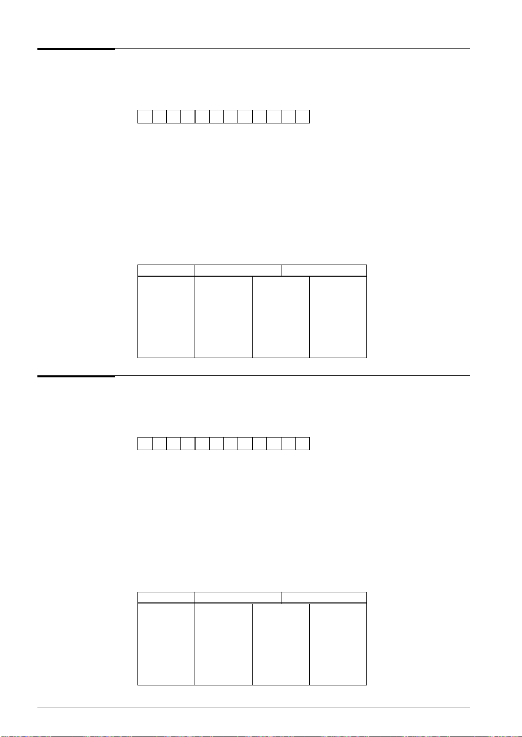
3 INSTRUCTION SET
ACPX MX,r Add with carry r-register to M(X), increment X by 1
Source Format:
Operation:
OP-Code:
Type:
Clock Cycles:
Flag:
Description:
Example:
ACPX MX,r
M(X) ← M(X) + r + C, X ← X + 1
1111001010r1 r0 F28H to F2BH
MSB LSB
V
7
C –
Set if a carry is generated; otherwise, reset.
Z –
Set if the result is zero; otherwise, reset.
D –
Not affected
I –
Not affected
Adds the carry bit and the contents of the r-register to the data memory location
addressed by IX. X is incremented by one. Incrementing X does not affect the
flags.
ACPX MX,A ACPX MX,MY
X register 1010 0000 1010 0001 1010 0010
Y register 0100 0110 0100 0110 0100 0110
Memory (A0H) 0110 1111 1111
Memory (A1H) 0011 0011 0111
Memory (46H) 0100 0100 0100
A register 1000 1000 1000
C flag 1 0 0
Z flag 0 0 0
ACPY MY,r Add with carry r-register to M(Y), increment Y by 1
Source Format:
Operation:
OP-Code:
Type:
Clock Cycles:
Flag:
Description:
Example:
ACPY MY,r
M(Y) ← M(Y) + r + C, Y ← Y + 1
1111001011r1 r0 F2CH to F2FH
MSB LSB
V
7
C –
Set if a carry is generated; otherwise, reset.
Z –
Set if the result is zero; otherwise, reset.
D –
Not affected
I –
Not affected
Adds the carry bit and the contents of the r-register to the data memory location
addressed by IY. Y is incremented by one. Incrementing Y does not affect the
flags.
ACPY MY,A ACPY MY,MX
X register 0010 0001 0010 0001 0010 0001
Y register 0000 1110 0000 1111 0001 0000
Memory (0EH) 1000 1011 1011
Memory (0FH) 0100 0100 1010
Memory (21H) 0110 0110 0110
A register 0010 0010 0010
C flag 1 0 0
Z flag 0 0 0
28 EPSON S1C6200/6200A CORE CPU MANUAL
Page 35
ADC r,i Add with carry immediate data i to r-register
3 INSTRUCTION SET
Source Format:
Operation:
OP-Code:
Type:
Clock Cycles:
Flag:
Description:
Example:
ADC r,i
r ← r + i
MSB LSB
3 to i0 + C
110001r
1 r0 i3 i2 i1 i0 C40H to C7FH
II
7
C –
Set if a carry is generated; otherwise, reset.
Z –
Set if the result is zero; otherwise, reset.
D –
Not affected
I –
Not affected
Adds the carry bit and immediate data i to the r-register.
ADC MX,3 ADC B,7
Memory (MX) 0100 1000 1000
B register 1001 1001 0000
C flag 1 0 1
Z flag 1 0 1
ADC r,q Add with carry q-register to r-register
Source Format:
Operation:
OP-Code:
Type:
Clock Cycles:
Flag:
Description:
Example:
ADC r,q
r ← r + q + C
10101001r1 r0 q1 q0 A90H to A9FH
MSB LSB
IV
7
C –
Set if a carry is generated; otherwise, reset.
Z –
Set if the result is zero; otherwise, reset.
D –
Not affected
I –
Not affected
Adds the carry bit and the contents of the q-register to the r-register.
ADC MY,A ADC MX,B
A register 0101 0101 0101
B register 0001 0001 0001
Memory (MX) 0111 0111 1001
Memory (MY) 1011 0001 0001
C flag 1 1 0
Z flag 0 0 0
S1C6200/6200A CORE CPU MANUAL EPSON 29
Page 36

3 INSTRUCTION SET
ADC XH,i Add with carry immediate data i to XH
Source Format:
Operation:
OP-Code:
Type:
Clock Cycles:
Flag:
Description:
Example:
ADC XH,i
XH ← XH + i
10100000i
MSB LSB
3 to i0 + C
3 i2 i1 i0 A00H to A0FH
IV
7
C –
Set if a carry is generated; otherwise, reset.
Z –
Set if the result is zero; otherwise, reset.
D –
Not affected
I –
Not affected
Adds the carry bit and immediate data i to XH, the four high-order bits of XHL.
ADC XH,2 ADC XH,4
XH register 1001 1100 0000
C flag 1 0 1
Z flag 0 0 1
ADC XL,i Add with carry immediate data i to XL
Source Format:
Operation:
OP-Code:
Type:
Clock Cycles:
Flag:
Description:
Example:
ADC XL,i
XL ← XL + i
10100001i
MSB LSB
3 to i0 + C
3 i2 i1 i0 A10H to A1FH
IV
7
C –
Set if a carry is generated; otherwise, reset.
Z –
Set if the result is zero; otherwise, reset.
D –
Not affected
I –
Not affected
Adds the carry bit and immediate data i to XL, the four low-order bits of XHL.
ADC XL,3 ADC XL,0EH
XL register 0000 0100 0010
C flag 1 0 1
Z flag 1 0 0
30 EPSON S1C6200/6200A CORE CPU MANUAL
Page 37

ADC YH,i Add with carry immediate data i to YH
3 INSTRUCTION SET
Source Format:
Operation:
OP-Code:
Type:
Clock Cycles:
Flag:
Description:
Example:
ADC YH,i
YH ← YH + i
10100010i
MSB LSB
3 to i0 + C
3 i2 i1 i0 A20H to A2FH
IV
7
C –
Set if a carry is generated; otherwise, reset.
Z –
Set if the result is zero; otherwise, reset.
D –
Not affected
I –
Not affected
Adds the carry bit and immediate data i to YH, the four high-order bits of YHL.
ADC YH,3 ADC YH,6
YH register 1010 1110 0100
C flag 1 0 1
Z flag 0 0 0
ADC YL,i Add with carry immediate data i to YL
Source Format:
Operation:
OP-Code:
Type:
Clock Cycles:
Flag:
Description:
Example:
ADC YL,i
YL ← YL + i
10100011i
MSB LSB
3 to i0 + C
3 i2 i1 i0 A30H to A3FH
IV
7
C –
Set if a carry is generated; otherwise, reset.
Z –
Set if the result is zero; otherwise, reset.
D –
Not affected
I –
Not affected
Adds the carry bit and immediate data i to YL, the four low-order bits of YHL.
ADC YL,3 ADC YL,2
YL register 1010 1110 0000
C flag 1 0 1
Z flag 0 0 1
S1C6200/6200A CORE CPU MANUAL EPSON 31
Page 38

3 INSTRUCTION SET
ADD r,i Add immediate data i to r-register
Source Format:
Operation:
OP-Code:
Type:
Clock Cycles:
Flag:
Description:
Example:
ADD r,i
r ← r + i
3 to i0
110000r1 r0 i3 i2 i1 i0 C00H to C3FH
MSB LSB
II
7
C –
Set if a carry is generated; otherwise, reset.
Z –
Set if the result is zero; otherwise, reset.
D –
Not affected
I –
Not affected
Adds immediate data i to the contents of the r-register.
ADD A,5 ADD MY,2
A register 1010 1111 1111
Memory (MY) 0110 0110 1000
C flag 1 0 0
Z flag 0 0 0
ADD r,q Add q-register to r-register
Source Format:
Operation:
OP-Code:
Type:
Clock Cycles:
Flag:
Description:
Example:
ADD r,q
r ← r + q
10101000r1 r0 q1 q0 A80H to A8FH
MSB LSB
IV
7
C –
Set if a carry is generated; otherwise, reset.
Z –
Set if the result is zero; otherwise, reset.
D –
Not affected
I –
Not affected
Adds the contents of the q-register to the contents of the r-register.
ADD A,MY ADD MX,B
A register 0010 1111 1111
B register 0100 0100 0100
Memory (MX) 0111 0111 1011
Memory (MY) 1101 1101 1101
C flag 1 0 0
Z flag 1 0 0
32 EPSON S1C6200/6200A CORE CPU MANUAL
Page 39

AND r,i Logical AND immediate data i with r-register
3 INSTRUCTION SET
Source Format:
Operation:
OP-Code:
Type:
Clock Cycles:
Flag:
Description:
Example:
AND r,i
r ← r ∧ i
3 to i0
110010r1 r0 i3 i2 i1 i0 C80H to CBFH
MSB LSB
II
7
C –
Not affected
Z –
Set if the result is zero; otherwise, reset.
D –
Not affected
I –
Not affected
Performs a logical AND operation between immediate data i and the contents of
the r-register. The result is stored in the r-register.
AND A,5 AND MX,3
A register 0110 0100 0100
Memory (MX) 1000 1000 0000
C flag 1 1 1
Z flag 0 0 1
AND r,q Logical AND q-register with r-register
Source Format:
Operation:
OP-Code:
Type:
Clock Cycles:
Flag:
Description:
Example:
AND r,q
r ← r ∧ q
10101100r1 r0 q1 q0 AC0H to ACFH
MSB LSB
IV
7
C –
Not affected
Z –
Set if the result is zero; otherwise, reset.
D –
Not affected
I –
Not affected
Performs a logical AND operation between the contents of the q-register and the
contents of the r-register. The result is stored in the r-register.
AND MX,A AND B,MY
A register 0100 0100 0100
B register 1011 1011 0010
Memory (MX) 1010 0000 0000
Memory (MY) 0010 0010 0010
C flag 0 0 0
Z flag 0 1 0
S1C6200/6200A CORE CPU MANUAL EPSON 33
Page 40
3 INSTRUCTION SET
CALL s Call subroutine
Source Format:
Source Format:
Operation:
Operation:
OP-Code:
OP-Code:
Type:
Type:
Clock Cycles:
Clock Cycles:
Flag:
Flag:
Description:
Description:
Example:
Example:
CALL s
M(SP-1) ← PCP, M(SP-2) ← PCSH, M(SP-3) ← PCSL + 1, SP ← SP - 3,
PCP ← NPP, PCS ← s
MSB LSB
0100s7 s6 s5 s4 s3 s2 s1 s0 400H to 4FFH
MSB LSB
7 to s0
I
7
C –
C –
Z –
Not affected
Z –
D –
Not affected
D –
I –
Not affected
I –
Not affected
Pushes the program counter (PCP, PCS) onto the stack as the return address,
then calls the subroutine addressed by NPP and the 8-bit operand.
PSET 06H CALL 10H
PCP 0011 0011 0110
PCS 0010 1100 0010 1100 0001 0000
NPP 0001 0110 0110
SP C0 C0 BD
Memory (SP-1) xxxx xxxx 0011
Memory (SP-2) xxxx xxxx 0010
Memory (SP-3) xxxx xxxx 1101
CALZ s Call subroutine at page zero
Source Format:
Source Format:
Operation:
Operation:
OP-Code:
OP-Code:
Type:
Type:
Clock Cycles:
Clock Cycles:
Flag:
Flag:
Description:
Description:
Example:
Example:
CALZ s
M(SP-1) ← PCP, M(SP-2) ← PCSH, M(SP-3) ← PCSL + 1, SP ← SP - 3,
PCP ← 0, PCS ← s
MSB LSB
0101s7 s6 s5 s4 s3 s2 s1 s0 500H to 5FFH
MSB LSB
7 to s0
I
7
C –
C –
Z –
Not affected
Z –
D –
Not affected
D –
I –
Not affected
I –
Not affected
Pushes the program counter (PCP, PCS) onto the stack as the return address,
then calls the subroutine addressed by the 8-bit operand. As NPP is reset to 0H,
only a subroutine in page 0 can be called.
CALZ 10H
PCP 1010 0000
PCS 0010 1110 0001 0000
SP CA C7
Memory (SP-1) xxxx 1010
Memory (SP-2) xxxx 0010
Memory (SP-3) xxxx 1111
34 EPSON S1C6200/6200A CORE CPU MANUAL
Page 41

CP r,i Compare immediate data i with r-register
3 INSTRUCTION SET
Source Format:
Source Format:
Operation:
Operation:
OP-Code:
OP-Code:
Type:
Type:
Clock Cycles:
Clock Cycles:
Flag:
Flag:
Description:
Description:
Example:
Example:
CP r,i
r - i
3 to i0
110111r1 r0 i3 i2 i1 i0 DC0H to DFFH
MSB LSB
II
7
C –
Set if r < i3 to i0; otherwise, reset.
Z –
Set if r = i
D –
Not affected
I –
Not affected
3 to i0; otherwise, reset.
Compares immediate data i to the r-register by subtracting i from the contents of r.
The r-register remains unchanged.
1. When Z = 0 and C = 0 then i < r
2. When Z = 1 and C = 0 then i = r
3. When Z = 0 and C = 1 then i > r
CP A,4 CP MX,7 CP B,2
A register 0100 0100 0100 0100
B register 1010 1010 1010 1010
Memory (MX) 0010 0010 0010 0010
C flag 1 0 1 0
Z flag 0 1 0 0
CP r,q Compare q-register with r-register
Source Format:
Source Format:
Operation:
Operation:
OP-Code:
OP-Code:
Type:
Type:
Clock Cycles:
Clock Cycles:
Flag:
Flag:
Description:
Description:
Example:
Example:
CP r,q
r - q
11110000r1 r0 q1 q0 F00H to F0FH
MSB LSB
IV
7
C –
Set if r < q; otherwise, reset.
Z –
Set if r = q; otherwise, reset.
D –
Not affected
I –
Not affected
Compares the q-register to the r-register by subtracting the contents of q from the
contents of r. The registers remain unchanged.
1. When Z = 0 and C = 0 then q < r
2. When Z = 1 and C = 0 then q = r
3. When Z = 0 and C = 1 then q > r
CP A,B CP MY,A
A register 1000 1000 1000
B register 0100 0100 0100
Memory (MY) 0111 0111 0111
C flag 0 0 1
Z flag 0 0 0
S1C6200/6200A CORE CPU MANUAL EPSON 35
Page 42

3 INSTRUCTION SET
CP XH,i Compare immediate data i with XH
Source Format:
Source Format:
Operation:
Operation:
OP-Code:
OP-Code:
Type:
Type:
Clock Cycles:
Clock Cycles:
Flag:
Flag:
Description:
Description:
Example:
Example:
CP XH,i
XH - i
3 to i0
10100100i3 i2 i1 i0 A40H to A4FH
MSB LSB
IV
7
C –
Set if XH < i3 to i0; otherwise, reset.
Z –
Set if XH = i
D –
Not affected
I –
Not affected
3 to i0; otherwise, reset.
Compares immediate data i to XH by subtracting i from the contents of XH. XH
remains unchanged.
1. When Z = 0 and C = 0 then i < XH
2. When Z = 1 and C = 0 then i = XH
3. When Z = 0 and C = 1 then i > XH
CP XH,2 CP XH,4 CP XH,9
XH register 0100 0100 0100 0100
C flag 1 0 0 1
Z flag 0 0 1 0
CP XL,i Compare immediate data i with XL
Source Format:
Source Format:
Operation:
Operation:
OP-Code:
OP-Code:
Type:
Type:
Clock Cycles:
Clock Cycles:
Flag:
Flag:
Description:
Description:
Example:
Example:
CP XL,i
XL - i
3 to i0
10100101i3 i2 i1 i0 A50H to A5FH
MSB LSB
IV
7
C –
Set if XL < i3 to i0; otherwise, reset.
Z –
Set if XL = i
D –
Not affected
I –
Not affected
3 to i0; otherwise, reset.
Compares immediate data i to XL by subtracting i from the contents of XL. XL
remains unchanged.
1. When Z = 0 and C = 0 then i < XL
2. When Z = 1 and C = 0 then i = XL
3. When Z = 0 and C = 1 then i > XL
CP XL,7 CP XL,9 CP XL,0AH
XL register 1001 1001 1001 1001
C flag 0 0 0 1
Z flag 0 0 1 0
36 EPSON S1C6200/6200A CORE CPU MANUAL
Page 43

CP YH,i Compare immediate data i with YH
3 INSTRUCTION SET
Source Format:
Source Format:
Operation:
Operation:
OP-Code:
OP-Code:
Type:
Type:
Clock Cycles:
Clock Cycles:
Flag:
Flag:
Description:
Description:
Example:
Example:
CP YH,i
YH - i
3 to i0
10100110i3 i2 i1 i0 A60H to A6FH
MSB LSB
IV
7
C –
Set if YH < i3 to i0; otherwise, reset.
Z –
Set if YH = i
D –
Not affected
I –
Not affected
3 to i0; otherwise, reset.
Compares immediate data i to YH by subtracting i from the contents of YH. YH
remains unchanged.
1. When Z = 0 and C = 0 then i < YH
2. When Z = 1 and C = 0 then i = YH
3. When Z = 0 and C = 1 then i > YH
CP YH,0AH CP YH,3 CP YH,0FH
YH register 1010 1010 1010 1010
C flag 1 0 0 1
Z flag 0 1 0 0
CP YL,i Compare immediate data i with YL
Source Format:
Source Format:
Operation:
Operation:
OP-Code:
OP-Code:
Type:
Type:
Clock Cycles:
Clock Cycles:
Flag:
Flag:
Description:
Description:
Example:
Example:
CP YL,i
YL - i
3 to i0
10100111i3 i2 i1 i0 A70H to A7FH
MSB LSB
IV
7
C –
Set if YL < i3 to i0; otherwise, reset.
Z –
Set if YL = i
D –
Not affected
I –
Not affected
3 to i0; otherwise, reset.
Compares immediate data i to YL by subtracting i from the contents of YL. YL
remains unchanged.
1. When Z = 0 and C = 0 then i < YL
2. When Z = 1 and C = 0 then i = YL
3. When Z = 0 and C = 1 then i > YL
CP YL,5 CP YL,1 CP YL,4
YL register 0100 0100 0100 0100
C flag 0 1 0 0
Z flag 1 0 0 1
S1C6200/6200A CORE CPU MANUAL EPSON 37
Page 44
3 INSTRUCTION SET
DEC Mn
Source Format:
Operation:
OP-Code:
Clock Cycles:
Description:
Example:
Type:
Flag:
Decrement memory
DEC Mn
M(n
3 to n0) ← M(n3 to n0) - 1
11110111n
MSB LSB
IV
7
C –
Set if a borrow is generated; otherwise, reset.
Z –
Set if the result is zero; otherwise, reset.
D –
Not affected
I –
Not affected
Decrements the contents of the data memory location addressed by Mn by 1.
DEC M0 DEC M2 DEC M0FH
Memory (00H) 1001 1000 1000 1000
Memory (02H) 0000 0000 1111 1111
Memory (0FH) 0001 0001 0001 0000
C flag 1 0 1 0
Z flag 0 0 0 1
3 n2 n1 n0 F70H to F7FH
DEC SP Decrement stack pointer
Source Format:
Operation:
OP-Code:
Type:
Clock Cycles:
Flag:
Description:
Example:
DEC SP
SP ← SP - 1
111111001011 FCBH
MSB LSB
VI
5
C –
Not affected
Z –
Not affected
D –
Not affected
I –
Not affected
Decrements the contents of the stack pointer by 1. This operation does not affect
the flags.
DEC SP
Memory (SP) 1011 0001 1011 0000
C flag 0 0
Z flag 1 1
38 EPSON S1C6200/6200A CORE CPU MANUAL
Page 45
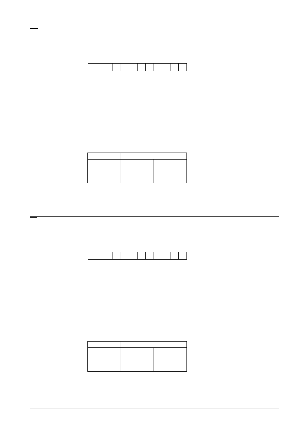
DI Disable interrupts
3 INSTRUCTION SET
Source Format:
Operation:
OP-Code:
Type:
Clock Cycles:
Flag:
Description:
Example:
DI
I ← 0
111101010111 F57H
MSB LSB
VI
7
C –
Not affected
Z –
Not affected
D –
Not affected
I –
Reset
Disables all interrupts.
DI
C flag 0 0
Z flag 1 1
D flag 0 0
I flag 1 0
EI Enable interrupts
Source Format:
Operation:
OP-Code:
Type:
Clock Cycles:
Flag:
Description:
Example:
EI
I ← 1
111101001000 F48H
MSB LSB
VI
7
C –
Not affected
Z –
Not affected
D –
Not affected
I –
Set
Enables all interrupts.
C flag 1 1
Z flag 0 0
D flag 0 0
I flag 0 1
EI
S1C6200/6200A CORE CPU MANUAL EPSON 39
Page 46

3 INSTRUCTION SET
FAN r,i Logical AND immediate data i with r-register for flag check
Source Format:
Operation:
OP-Code:
Type:
Clock Cycles:
Flag:
Description:
Example:
FAN r,i
r ∧ i
3 to i0
110110r1 r0 i3 i2 i1 i0 D80H to DBFH
MSB LSB
II
7
C –
Not affected
Z –
Set if the result is zero; otherwise, reset.
D –
Not affected
I –
Not affected
Performs a logical AND operation between immediate data i and the contents of
the r-register. Only the Z flag is affected. The r-register remains unchanged.
FAN A,7 FAN MY,9 FAN B,2
A register 1000 1000 1000 1000
B register 0100 0100 0100 0100
Memory (MY) 1000 1000 1000 1000
C flag 1 1 1 1
Z flag 0 1 0 1
FAN r,q Logical AND q-register with r-register for flag check
Source Format:
Operation:
OP-Code:
Type:
Clock Cycles:
Flag:
Description:
Example:
FAN r,q
r ∧ q
11110001r1 r0 q1 q0 F10H to F1FH
MSB LSB
IV
7
C –
Not affected
Z –
Set if the result is zero; otherwise, reset.
D –
Not affected
I –
Not affected
Performs a logical AND operation between the contents of the q-register and the
contents of the r-register. Only the Z flag is affected. The registers remains
unchanged.
FAN A,B FAN MX,B FAN A,MY
A register 1000 1000 1000 1000
B register 1010 1010 1010 1010
Memory (MX) 0101 0101 0101 0101
Memory (MY) 1110 1110 1110 1110
C flag 0 0 0 0
Z flag 0 0 1 0
40 EPSON S1C6200/6200A CORE CPU MANUAL
Page 47
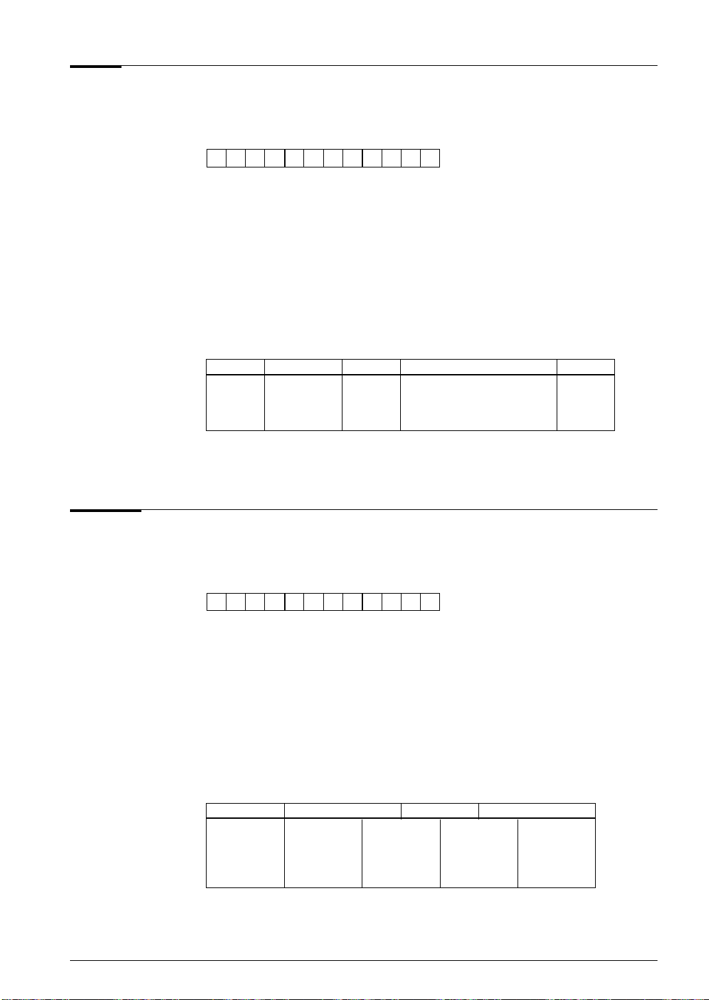
HALT Halt
3 INSTRUCTION SET
Source Format:
Operation:
OP-Code:
Type:
Clock Cycles:
Flag:
Description:
Example:
HALT
Stops CPU
111111111000 FF8H
MSB LSB
VI
5
C –
Not affected
Z –
Not affected
D –
Not affected
I –
Not affected
Stops the CPU. When an interrupt occurs, PCP and PCS are pushed onto the
stack as the return address and the interrupt service routine is executed.
Instruction State PCP PCS I flag
HALT RUN 0001 0011 0011 1
Interrupt 0001 0011 0100 1
HALT
RUN 0001 Interrupt vector address 0
INC Mn Increment memory by 1
Source Format:
Operation:
OP-Code:
Type:
Clock Cycles:
Flag:
Description:
Example:
INC Mn
M(n
3 to n0) ← M(n3 to n0) + 1
11110110n
MSB LSB
IV
7
C –
Set if a carry is generated; otherwise, reset.
Z –
Set if the result is zero; otherwise, reset.
D –
Not affected
I –
Not affected
The contents of the data memory location addressed by Mn is incremented by 1.
INC M1 INC M3 INC M0DH
Memory (01H) 0100 0101 0101 0101
Memory (03H) 1111 1111 0000 0000
Memory (0DH) 0111 0111 0111 1000
C flag 0 0 1 0
Z flag 1 0 1 0
3 n2 n1 n0 F60H to F6FH
S1C6200/6200A CORE CPU MANUAL EPSON 41
Page 48

3 INSTRUCTION SET
Increment stack pointer by 1INC SP
Source Format:
Operation:
OP-Code:
Type:
Clock Cycles:
Flag:
Description:
Example:
INC SP
SP ← SP + 1
111111011011 FDBH
MSB LSB
VI
5
C –
Not affected
Z –
Not affected
D –
Not affected
I –
Not affected
Increments the contents of the stack pointer by 1. This operation does not affect
the flags.
INC SP
SP 1110 1111 1111 0000
C flag 0 0
Z flag 0 0
INC X Increment X-register by 1
Source Format:
Operation:
OP-Code:
Type:
Clock Cycles:
Flag:
Description:
Example:
INC X
X ← X + 1
111011100000 EE0H
MSB LSB
VI
5
C –
Not affected
Z –
Not affected
D –
Not affected
I –
Not affected
Increments the contents of register X by 1. This operation does not affect the
flags.
INC X
X register 1111 1110 1111 1111
C flag 1 1
Z flag 0 0
42 EPSON S1C6200/6200A CORE CPU MANUAL
Page 49

INC Y Increment Y-register by 1
3 INSTRUCTION SET
Source Format:
Operation:
OP-Code:
Type:
Clock Cycles:
Flag:
Description:
Example:
INC Y
Y ← Y + 1
111011110000 EF0H
MSB LSB
VI
5
C –
Not affected
Z –
Not affected
D –
Not affected
I –
Not affected
Increments the contents of register Y by 1. This operation does not affect the
flags.
INC Y
Y register 1011 0111 1011 1000
C flag 1 1
Z flag 0 0
JPBA Indirect jump using registers A and B
Source Format:
Operation:
OP-Code:
Type:
Clock Cycles:
Flag:
Description:
Example:
JPBA
PCB ← NBP, PCP ← NPP, PCSH ← B, PCSL ← A
111111101000 FE8H
MSB LSB
VI
5
C –
Not affected
Z –
Not affected
D –
Not affected
I –
Not affected
Uses the contents of a- and b-registers to specify the destination address of the
jump. The b-register contains the four high-order bits of the address and the aregister contains the four low-order bits of the address.
PSET 15H JPBA
PCB 0 0 1
NBP 0 1 1
PCP 1000 1000 0101
NPP 0001 0101 0101
PCS 1001 0000 1001 0001 0000 0110
A register 0110 0110 0110
B register 0000 0000 0000
S1C6200/6200A CORE CPU MANUAL EPSON 43
Page 50

3 INSTRUCTION SET
JP C,s Jump if carry flag is set
Source Format:
Operation:
OP-Code:
Type:
Clock Cycles:
Flag:
Description:
Example:
JP C,s
PCB ← NBP, PCP ← NPP, PCS ← s
0010s
MSB LSB
7 s6 s5 s4 s3 s2 s1 s0 200H to 2FFH
7 to s0 if C = 1
I
5
C –
Not affected
Z –
Not affected
D –
Not affected
I –
Not affected
Jumps to the destination address specified by the 8-bit operand when the carry
flag is set.
ADD A,8 PSET 06H JP C,10H
PCB 0 0 0 0
NBP 0 0 0 0
PCP 0010 0010 0010 0110
NPP 0001 0001 0110 0110
PCS 0011 1100 0011 1101 0011 1110 0001 0000
A register 1000 0000 0000 0000
C flag 0 1 1 1
JP NC,s Jump if not carry
Source Format:
Operation:
OP-Code:
Type:
Clock Cycles:
Flag:
Description:
Example:
JP NC,s
PCB ← NBP, PCP ← NPP, PCS ← s
0011s
MSB LSB
7 s6 s5 s4 s3 s2 s1 s0 300H to 3FFH
I
5
C –
Not affected
Z –
Not affected
D –
Not affected
I –
Not affected
Jumps to the destination address specified by the 8-bit operand when the carry
flag is not set.
PSET 11H JP NC,10H
PCB 0 0 1
NBP 0 1 1
PCP 1001 1001 0001
NPP 0001 0001 0001
PCS 1000 1111 1001 0000 0001 0000
C flag 0 0 0
7 to s0 if C = 0
44 EPSON S1C6200/6200A CORE CPU MANUAL
Page 51

JP NZ,s Jump if not zero
3 INSTRUCTION SET
Source Format:
Operation:
OP-Code:
Type:
Clock Cycles:
Flag:
Description:
Example:
JP NZ,s
PCB ← NBP, PCP ← NPP, PCS ← s
0111s
MSB LSB
7 s6 s5 s4 s3 s2 s1 s0 700H to 7FFH
7 to s0 if Z = 0
I
5
C –
Not affected
Z –
Not affected
D –
Not affected
I –
Not affected
Jumps to the destination address specified by the 8-bit operand when the zero flag
is not set.
JP NZ,10H
PCB 1 1
NBP 1 1
PCP 0000 0000
NPP 0000 0000
PCS 0000 0111 0001 0000
Z flag 0 0
JP s Jump
Source Format:
Operation:
OP-Code:
Type:
Clock Cycles:
Flag:
Description:
Example:
JP s
PCB ← NBP, PCP ← NPP, PCS ← s
0000s7 s6 s5 s4 s3 s2 s1 s0 000H to 0FFH
MSB LSB
I
5
C –
Not affected
Z –
Not affected
D –
Not affected
I –
Not affected
Unconditional jump to the destination address specified by the 8-bit operand.
PCB 0 0 0
NBP 0 0 0
PCP 0000 0000 1010
NPP 0001 1010 1010
PCS 0100 0010 0100 0011 0001 0000
7 to s0
PSET 0AH JP 10H
S1C6200/6200A CORE CPU MANUAL EPSON 45
Page 52
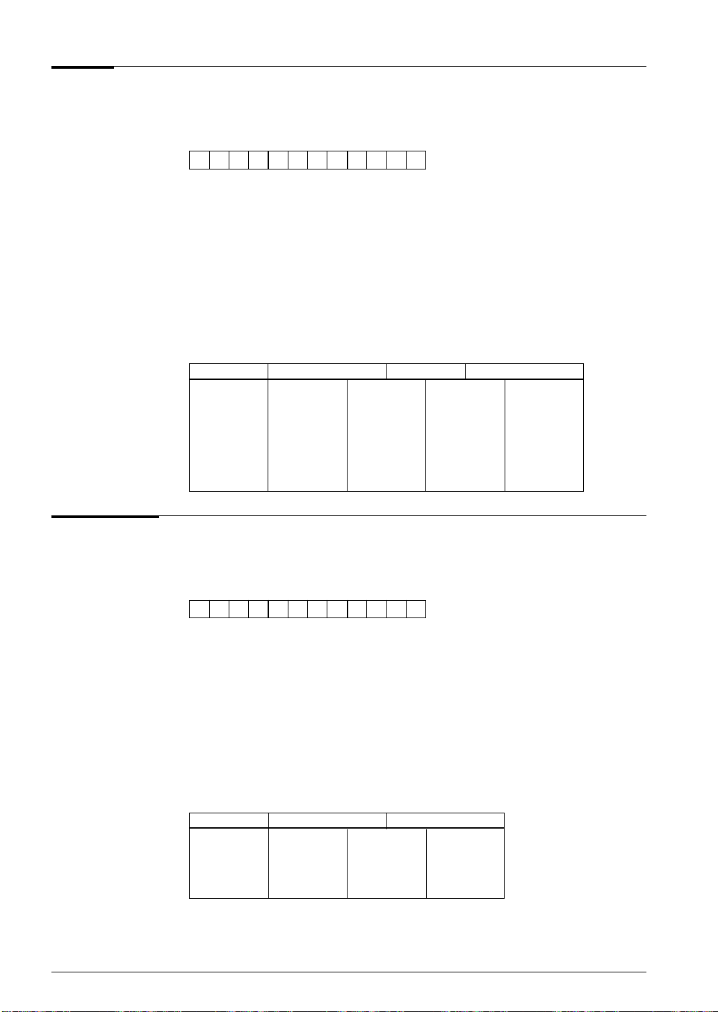
3 INSTRUCTION SET
JP Z,s Jump if zero
Source Format:
Operation:
OP-Code:
Type:
Clock Cycles:
Flag:
Description:
Example:
JP Z,s
PCB ← NBP, PCP ← NPP, PCS ← s
0110s
MSB LSB
7 s6 s5 s4 s3 s2 s1 s0 600H to 6FFH
7 to s0 if Z = 1
I
5
C –
Not affected
Z –
Not affected
D –
Not affected
I –
Not affected
Jumps to the destination address specified by the 8-bit operand when the zero flag
is set.
SUB A,B PSET 1BH JP Z,10H
PCB 0 0 0 1
NBP 0 0 1 1
PCP 0101 0101 0101 1011
NPP 0001 0001 1011 1011
PCS 0000 0010 0000 0011 0000 0100 0001 0000
A register 0110 0000 0000 0000
B register 0110 0110 0110 0110
Z flag 0 1 1 1
LBPX MX,e Load immediate data e to memory, and increment X by 2
Source Format:
Operation:
OP-Code:
Type:
Clock Cycles:
Flag:
Description:
Example:
LBPX MX,e
M(X) ← e
1001e
MSB LSB
3 to e0, M(X+1) ← e7 to e4, X ← X + 2
7 e6 e5 e4 e3 e2 e1 e0 900H to 9FFH
I
5
C –
Not affected
Z –
Not affected
D –
Not affected
I –
Not affected
Stores 8-bit immediate data e in two, consecutive 4-bit locations in data memory.
The X-register is incremented by 2. An overflow in X does not affect the flags.
LBPX MX,18H LBPX MX,36H
X register 0001 1110 0010 0000 0010 0010
Memory (1EH) 0010 1000 1000
Memory (1FH) 1111 0001 0001
Memory (20H) 0000 0000 0110
Memory (21H) 0111 0111 0011
46 EPSON S1C6200/6200A CORE CPU MANUAL
Page 53

LD A,Mn Load memory into A-register
3 INSTRUCTION SET
Source Format:
Operation:
OP-Code:
Type:
Clock Cycles:
Flag:
Description:
Example:
LD A,Mn
A ← M(n
11111010n
MSB LSB
3 to n0)
3 n2 n1 n0 FA0H to FAFH
IV
5
C –
Not affected
Z –
Not affected
D –
Not affected
I –
Not affected
Loads the contents of the data memory location addressed by Mn into the Aregister.
LD A,M5 LD A,M6
A register 0100 1111 0100
Memory (05H) 1111 1111 1111
Memory (06H) 0100 0100 0100
LD B,Mn Load memory into B-register
Source Format:
Operation:
OP-Code:
Type:
Clock Cycles:
Flag:
Description:
Example:
LD B,Mn
B ← M(n
11111011n
MSB LSB
3 to n0)
3 n2 n1 n0 FB0H to FBFH
IV
5
C –
Not affected
Z –
Not affected
D –
Not affected
I –
Not affected
Loads the contents of the data memory location addressed by Mn into the Bregister.
LD B,M7 LD B,M8
B register 0100 0110 1010
Memory (07H) 0110 0110 0110
Memory (08H) 1010 1010 1010
S1C6200/6200A CORE CPU MANUAL EPSON 47
Page 54
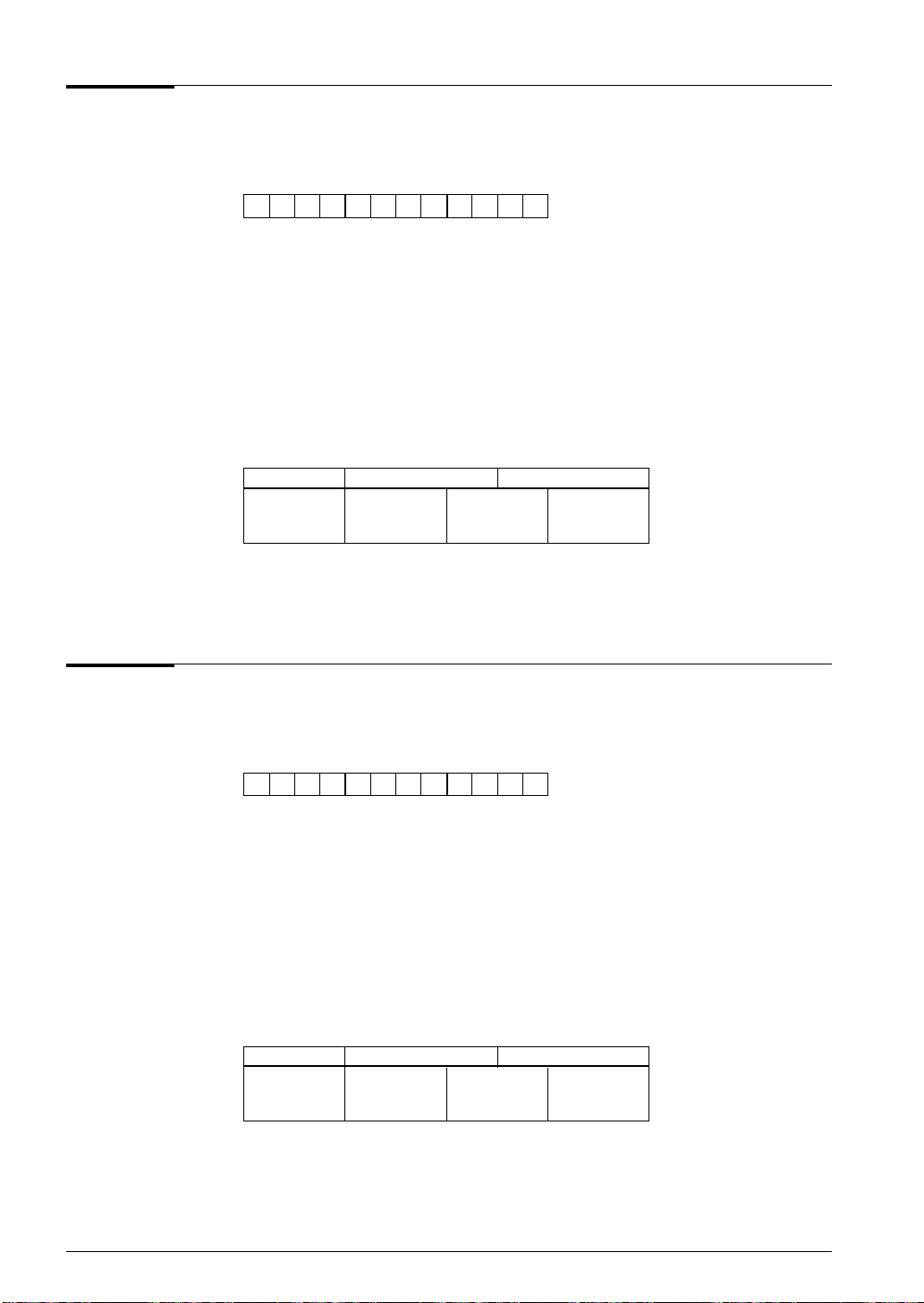
3 INSTRUCTION SET
LD Mn,A Load A-register into memory
Source Format:
Operation:
OP-Code:
Type:
Clock Cycles:
Flag:
Description:
Example:
LD Mn,A
M(n
3 to n0) ← A
11111000n
MSB LSB
3 n2 n1 n0 F80H to F8FH
IV
5
C –
Not affected
Z –
Not affected
D –
Not affected
I –
Not affected
Loads the contents of the A-register into the location addressed by Mn.
LD M0AH,A LD M0BH,A
A register 0110 0110 0110
Memory (0AH) 0100 0110 0110
Memory (0BH) 1011 1011 0110
LD Mn,B Load B-register into memory
Source Format:
Operation:
OP-Code:
Type:
Clock Cycles:
Flag:
Description:
Example:
LD Mn,B
M(n
3 to n0) ← B
11111001n
MSB LSB
3 n2 n1 n0 F90H to F9FH
IV
5
C –
Not affected
Z –
Not affected
D –
Not affected
I –
Not affected
Loads the contents of the B-register into the data memory location addressed by
Mn.
LD M0,B LD M1,B
B register 0100 0100 0100
Memory (00H) 1011 0100 0100
Memory (01H) 1111 1111 0100
48 EPSON S1C6200/6200A CORE CPU MANUAL
Page 55
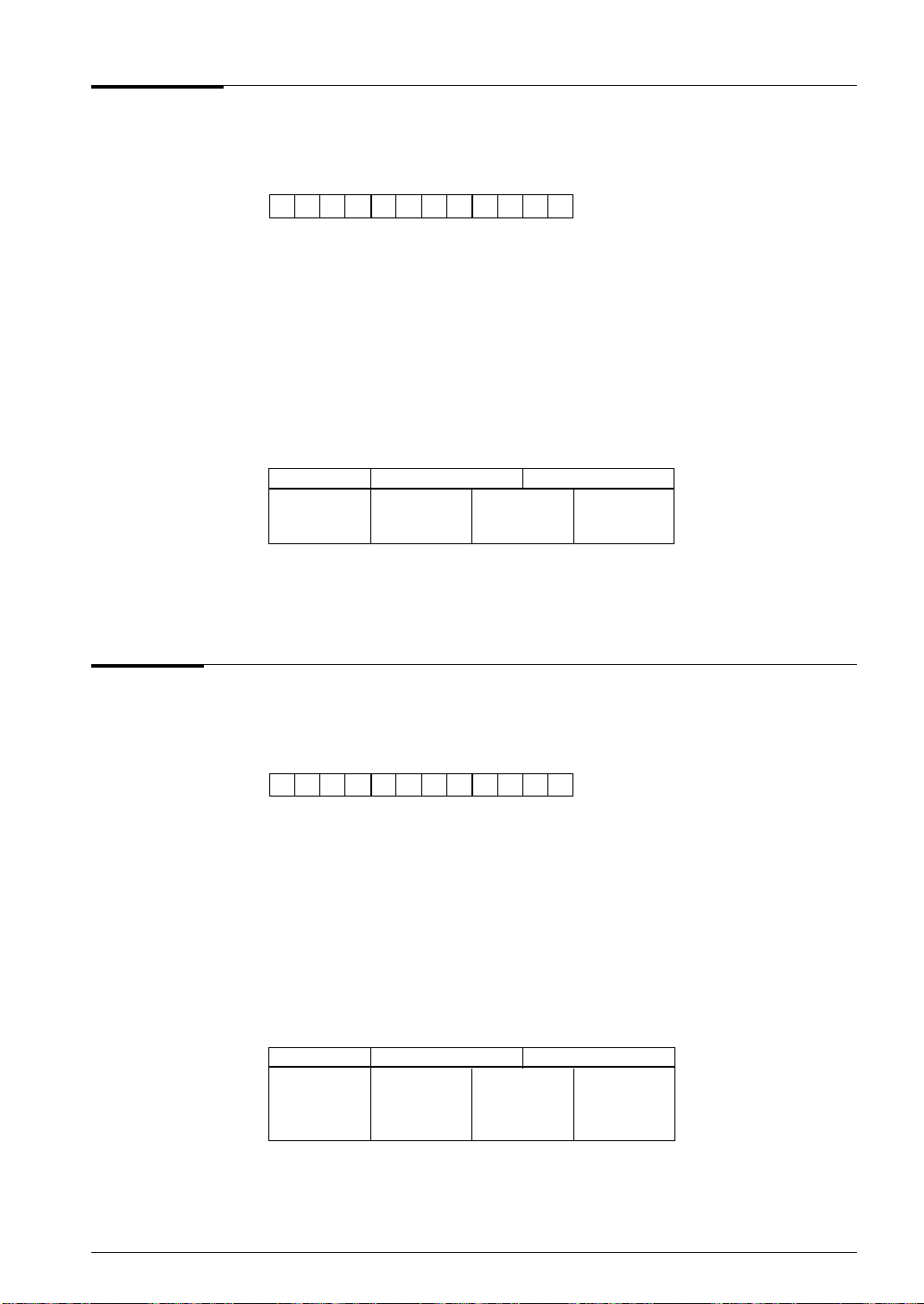
LDPX MX,i Load immediate data i into MX, increment X by 1
3 INSTRUCTION SET
Source Format:
Operation:
OP-Code:
Type:
Clock Cycles:
Flag:
Description:
Example:
LDPX MX,i
M(X) ← i
11100110 i
MSB LSB
3 to i0, X ← X + 1
3 i2 i1 i0 E60H to E6FH
IV
5
C –
Not affected
Z –
Not affected
D –
Not affected
I –
Not affected
Loads immediate data i into the data memory location addressed by IX. X is
incremented by 1. Incrementing X does not affect the flags.
LDPX MX,7 LDPX MX,0AH
X register 1000 0011 1000 0100 1000 0101
Memory (83H) 0010 0111 0111
Memory (84H) 1001 1001 1010
LDPX r,q Load q-register into r-register, increment X by 1
Source Format:
Operation:
OP-Code:
Type:
Clock Cycles:
Flag:
Description:
Example:
LDPX r,q
r ← q, X ← X + 1
11101110 r1 r0 q1 q0 EE0H to EEFH
MSB LSB
IV
5
C –
Not affected
Z –
Not affected
D –
Not affected
I –
Not affected
Loads the contents of the q-register into the r-register. X is incremented by 1.
Incrementing X does not affect the flags.
LDPX A,B LDPX B,MY
X register 0100 1001 0100 1010 0100 1011
A register 1010 1101 1101
B register 1101 1101 0000
Memory (MY) 0000 0000 0000
S1C6200/6200A CORE CPU MANUAL EPSON 49
Page 56

3 INSTRUCTION SET
LDPY MY,i Load immediate data i into MY, increment Y by 1
Source Format:
Operation:
OP-Code:
Type:
Clock Cycles:
Flag:
Description:
Example:
LDPY MY,i
M(Y) ← i
11100111 i
MSB LSB
3 to i0, Y ← Y + 1
3 i2 i1 i0 E70H to E7FH
IV
5
C –
Not affected
Z –
Not affected
D –
Not affected
I –
Not affected
Loads immediate data i into the data memory location addressed by IY. Y is
incremented by 1. Incrementing Y does not affect the flags.
LDPY MY,7 LDPY MY,0
Y register 0010 1101 0010 1110 0010 1111
Memory (2DH) 1010 0111 0111
Memory (2EH) 0010 0010 0000
LDPY r,q Load q-register into r-register, increment Y by 1
Source Format:
Operation:
OP-Code:
Type:
Clock Cycles:
Flag:
Description:
Example:
LDPY r,q
r ← q, Y ← Y + 1
11101111 r1 r0 q1 q0 EF0H to EFFH
MSB LSB
IV
5
C –
Not affected
Z –
Not affected
D –
Not affected
I –
Not affected
Loads the contents of the q-register into the r-register. Y is incremented by 1.
Incrementing Y does not affect the flags.
LDPY A,B LDPY MX,B
Y register 0100 1000 0100 1001 0100 1010
A register 1010 1000 1000
B register 1000 1000 1000
Memory (MX) 0010 0010 1000
50 EPSON S1C6200/6200A CORE CPU MANUAL
Page 57
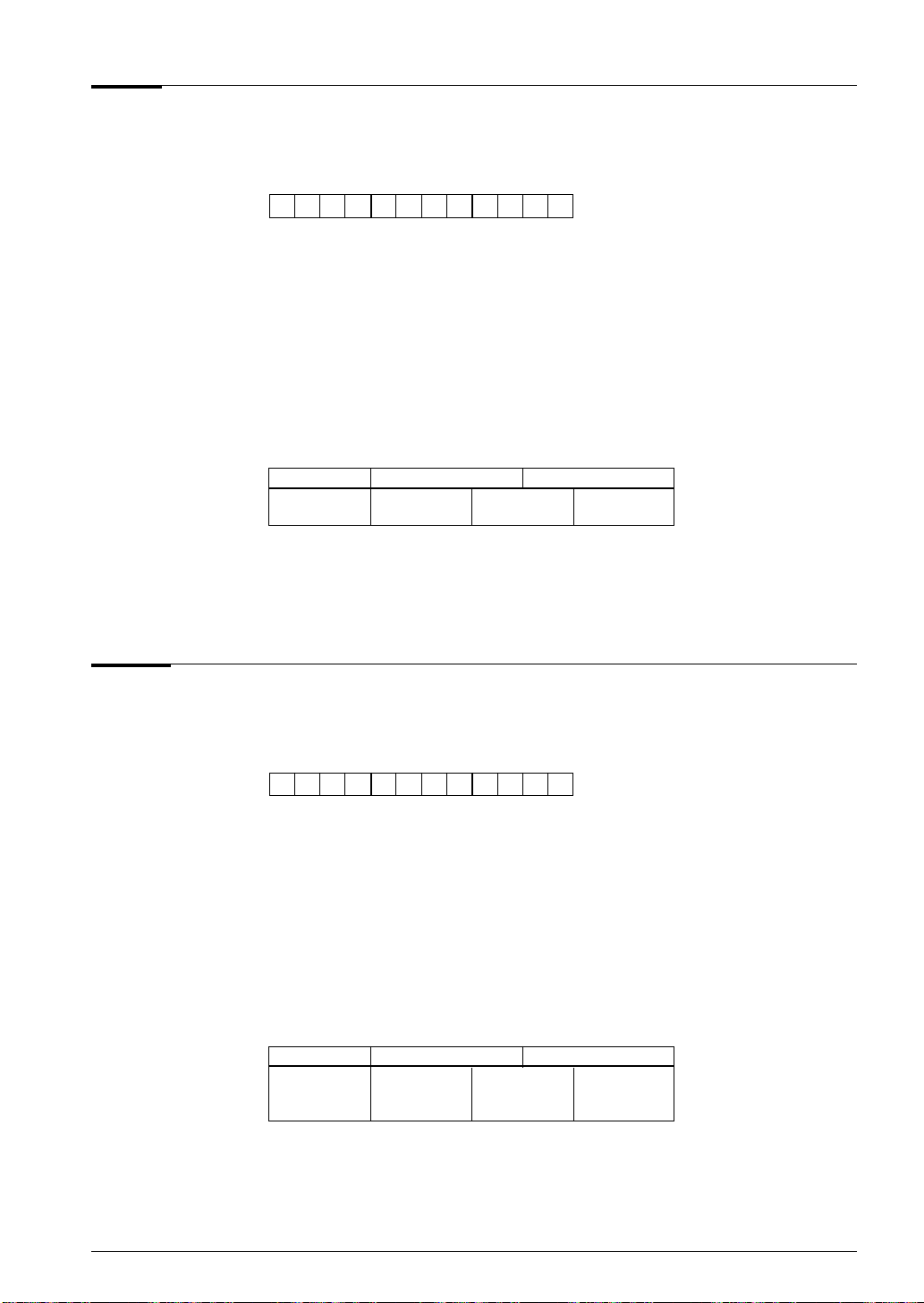
LD r,i Load immediate data i into r-register
3 INSTRUCTION SET
Source Format:
Operation:
OP-Code:
Type:
Clock Cycles:
Flag:
Description:
Example:
LD r,i
r ← i
3 to i0
111000r1 r0 i3 i2 i1 i0 E00H to E3FH
MSB LSB
II
5
C –
Not affected
Z –
Not affected
D –
Not affected
I –
Not affected
Loads immediate data i into the r-register.
LD A,6 LD MY,0
A register 0101 0110 0110
Memory (MY) 1001 1001 0000
LD r,q Load q-register into r-register
Source Format:
Operation:
OP-Code:
Type:
Clock Cycles:
Flag:
Description:
Example:
LD r,q
r ← q
11101100r1 r0 q1 q0 EC0H to ECFH
MSB LSB
IV
5
C –
Not affected
Z –
Not affected
D –
Not affected
I –
Not affected
The contents of the q-register are loaded into the r-register.
LD A,B LD B,MY
A register 0010 0000 0000
B register 0000 0000 0110
Memory (MY) 0110 0110 0110
S1C6200/6200A CORE CPU MANUAL EPSON 51
Page 58

3 INSTRUCTION SET
LD r,SPH Load SPH into r-register
Source Format:
Operation:
OP-Code:
Type:
Clock Cycles:
Flag:
Description:
Example:
LD r,SPH
r ← SPH
1111111001r1 r0 FE4H to FE7H
MSB LSB
V
5
C –
Not affected
Z –
Not affected
D –
Not affected
I –
Not affected
Loads the four high-order bits of the stack pointer into the r-register.
LD MX,SPH LD A,SPH
SPH 0111 0111 0111
A register 0000 0000 0111
Memory (MX) 1100 0111 0111
LD r,SPL Load SPL into r-register
Source Format:
Operation:
OP-Code:
Type:
Clock Cycles:
Flag:
Description:
Example:
LD r,SPL
r ← SPL
1111111101r1 r0 FF4H to FF7H
MSB LSB
V
5
C –
Not affected
Z –
Not affected
D –
Not affected
I –
Not affected
Loads the four low-order bits of the stack pointer into the r-register.
LD A,SPL LD MY,SPL
SPL 1001 1001 1001
A register 0010 1001 1001
Memory (MY) 0000 0000 1001
52 EPSON S1C6200/6200A CORE CPU MANUAL
Page 59

LD r,XH Load XH into r-register
3 INSTRUCTION SET
Source Format:
Operation:
OP-Code:
Type:
Clock Cycles:
Flag:
Description:
Example:
LD r,XH
r ← XH
1110101001r1 r0 EA4H to EA7H
MSB LSB
V
5
C –
Not affected
Z –
Not affected
D –
Not affected
I –
Not affected
Loads the four high-order bits of register X into the r-register.
LD B,XH LD MX,XH
XH register 1010 1010 1010
B register 0010 1010 1010
Memory (MX) 0000 0000 1010
LD r,XL Load XL into r-register
Source Format:
Operation:
OP-Code:
Type:
Clock Cycles:
Flag:
Description:
Example:
LD r,XL
r ← XL
1110101010r1 r0 EA8H to EABH
MSB LSB
V
5
C –
Not affected
Z –
Not affected
D –
Not affected
I –
Not affected
Loads the four low-order bits of register X into the r-register.
LD MY,XL LD A,XL
XL register 0000 0000 0000
A register 1101 1101 0000
Memory (MY) 0001 0000 0000
S1C6200/6200A CORE CPU MANUAL EPSON 53
Page 60

3 INSTRUCTION SET
LD r,XP Load XP into r-register
Source Format:
Operation:
OP-Code:
Type:
Clock Cycles:
Flag:
Description:
Example:
LD r,XP
r ← XP
1110101000r1 r0 EA0H to EA3H
MSB LSB
V
5
C –
Not affected
Z –
Not affected
D –
Not affected
I –
Not affected
Loads the 4-bit page part of index register IX into the r-register.
LD MX,XP LD A,XP
XP register 1111 1111 1111
A register 0010 0010 1111
Memory (MX) 0101 1111 1111
LD r,YH Load YH into r-register
Source Format:
Operation:
OP-Code:
Type:
Clock Cycles:
Flag:
Description:
Example:
LD r,YH
r ← YH
1110101101r1 r0 EB4H to EB7H
MSB LSB
V
5
C –
Not affected
Z –
Not affected
D –
Not affected
I –
Not affected
Loads the four high-order bits of register Y into the r-register.
LD A,YH LD MY,YH
YH register 1010 1010 1010
A register 1100 1010 1010
Memory (MY) 1110 1110 1010
54 EPSON S1C6200/6200A CORE CPU MANUAL
Page 61

LD r,YL Load YL into r-register
3 INSTRUCTION SET
Source Format:
Operation:
OP-Code:
Type:
Clock Cycles:
Flag:
Description:
Example:
LD r,YL
r ← YL
1110101110r1 r0 EB8H to EBBH
MSB LSB
V
5
C –
Not affected
Z –
Not affected
D –
Not affected
I –
Not affected
Loads the four low-order bits of register Y into the r-register.
LD B,YL LD MX,YL
YL register 0000 0000 0000
B register 0110 0000 0000
Memory (MX) 1011 1011 0000
LD r,YP Load YP into r-register
Source Format:
Operation:
OP-Code:
Type:
Clock Cycles:
Flag:
Description:
Example:
LD r,YP
r ← YP
1110101100r1 r0 EB0H to EB3H
MSB LSB
V
5
C –
Not affected
Z –
Not affected
D –
Not affected
I –
Not affected
Loads the 4-bit page part of index register IY into the r-register.
LD MY,YP LD B,YP
YP register 1010 1010 1010
B register 1100 1100 1010
Memory (MY) 0110 1010 1010
S1C6200/6200A CORE CPU MANUAL EPSON 55
Page 62

3 INSTRUCTION SET
LD SPH,r Load r-register into SPH
Source Format:
Operation:
OP-Code:
Type:
Clock Cycles:
Flag:
Description:
Example:
LD SPH,r
SPH ← r
1111111000r1 r0 FE0H to FE3H
MSB LSB
V
5
C –
Not affected
Z –
Not affected
D –
Not affected
I –
Not affected
Loads the contents of the r-register into the four high-order bits of the stack
pointer.
LD SPH,A LD SPH,MY
SPH 1001 0011 1100
A register 0011 0011 0011
Memory (MY) 1100 1100 1100
LD SPL,r Load r-register into SPL
Source Format:
Operation:
OP-Code:
Type:
Clock Cycles:
Flag:
Description:
Example:
LD SPL,r
SPL ← r
1111111100r1 r0 FF0H to FF3H
MSB LSB
V
5
C –
Not affected
Z –
Not affected
D –
Not affected
I –
Not affected
Loads the contents of the r-register into the four low-order bits of the stack pointer.
LD SPL,B LD SPL,MX
SPL 1011 0111 1111
B register 0111 0111 0111
Memory (MX) 1111 1111 1111
56 EPSON S1C6200/6200A CORE CPU MANUAL
Page 63

LD X,e Load immediate data e into X-register
3 INSTRUCTION SET
Source Format:
Operation:
OP-Code:
Type:
Clock Cycles:
Flag:
Description:
Example:
LD X,e
XH ← e
7 to e4, XL ← e3 to e0
1011e7 e6 e5 e4 e3 e2 e1 e0 B00H to BFFH
MSB LSB
I
5
C –
Not affected
Z –
Not affected
D –
Not affected
I –
Not affected
Loads 8-bit immediate data e into register X.
LD X,6FH
XH register 0000 0110
XL register 1011 1111
LD XH,r Load r-register into XH
Source Format:
Operation:
OP-Code:
Type:
Clock Cycles:
Flag:
Description:
Example:
LD XH,r
XH ← r
1110100001r1 r0 E84H to E87H
MSB LSB
V
5
C –
Not affected
Z –
Not affected
D –
Not affected
I –
Not affected
Loads the contents of the r-register into the four high-order bits of register X.
LD XH,A LD XH,MY
XH register 0000 1011 0110
A register 1011 1011 1011
Memory (MY) 0110 0110 0110
S1C6200/6200A CORE CPU MANUAL EPSON 57
Page 64
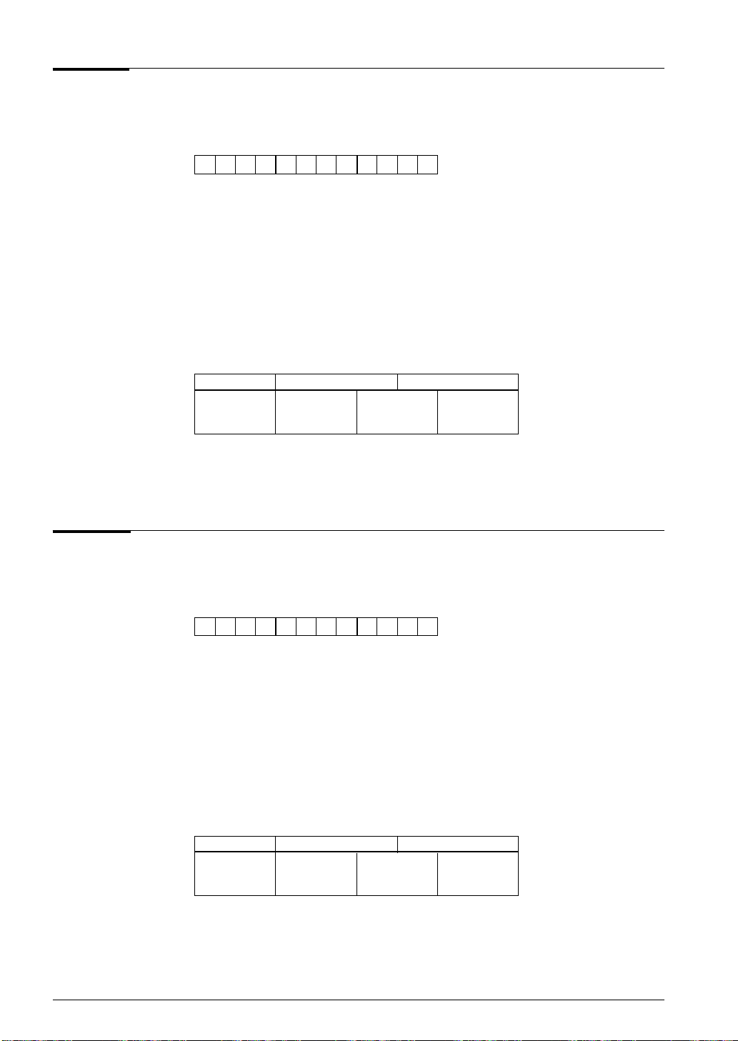
3 INSTRUCTION SET
LD XL,r Load r-register into XL
Source Format:
Operation:
OP-Code:
Type:
Clock Cycles:
Flag:
Description:
Example:
LD XL,r
XL ← r
1110100010r1 r0 E88H to E8BH
MSB LSB
V
5
C –
Not affected
Z –
Not affected
D –
Not affected
I –
Not affected
Loads the contents of the r-register into the four low-order bits of register X.
LD XL,MY LD XL,A
XL register 0000 0010 1011
A register 1011 1011 1011
Memory (MY) 0010 0010 0010
LD XP,r Load r-register into XP
Source Format:
Operation:
OP-Code:
Type:
Clock Cycles:
Flag:
Description:
Example:
LD XP,r
XP ← r
1110100000r1 r0 E80H to E83H
MSB LSB
V
5
C –
Not affected
Z –
Not affected
D –
Not affected
I –
Not affected
Loads the contents of the r-register into the 4-bit page part of index register IX.
LD XP,B LD XP,MX
XP register 1001 0001 1011
B register 0001 0001 0001
Memory (MX) 1011 1011 1011
58 EPSON S1C6200/6200A CORE CPU MANUAL
Page 65

LD Y,e Load immediate data e into Y-register
3 INSTRUCTION SET
Source Format:
Operation:
OP-Code:
Type:
Clock Cycles:
Flag:
Description:
Example:
LD Y,e
YH ← e
7 to e4, YL ← e3 to e0
1000e7 e6 e5 e4 e3 e2 e1 e0 800H to 8FFH
MSB LSB
I
5
C –
Not affected
Z –
Not affected
D –
Not affected
I –
Not affected
Loads 8-bit immediate data e into register Y.
LD Y,E1H
YH register 0001 1110
YL register 1100 0001
LD YH,r Load r-register into YH
Source Format:
Operation:
OP-Code:
Type:
Clock Cycles:
Flag:
Description:
Example:
LD YH,r
YH ← r
1110100101r1 r0 E94H to E97H
MSB LSB
V
5
C –
Not affected
Z –
Not affected
D –
Not affected
I –
Not affected
Loads the contents of the r-register into the four high-order bits of register Y.
LD YH,B LD YH,MX
YH register 0000 0110 0101
B register 0110 0110 0110
Memory (MX) 0101 0101 0101
S1C6200/6200A CORE CPU MANUAL EPSON 59
Page 66

3 INSTRUCTION SET
LD YL,r Load r-register into YL
Source Format:
Operation:
OP-Code:
Type:
Clock Cycles:
Flag:
Description:
Example:
LD YL,r
YL ← r
1110100110r1 r0 E98H to E9BH
MSB LSB
V
5
C –
Not affected
Z –
Not affected
D –
Not affected
I –
Not affected
Loads the contents of the r-register into the four low-order bits of register Y.
LD YL,B LD YL,MX
YL register 1011 1010 0111
B register 1010 1010 1010
Memory (MX) 0111 0111 0111
LD YP,r Load r-register into YP
Source Format:
Operation:
OP-Code:
Type:
Clock Cycles:
Flag:
Description:
Example:
LD YP,r
YP ← r
1110100100r1 r0 E90H to E93H
MSB LSB
V
5
C –
Not affected
Z –
Not affected
D –
Not affected
I –
Not affected
Loads the contents of the r-register into the 4-bit page part of index register IY.
LD YP,MX LD YP,A
YP register 0011 0000 0100
A register 0100 0100 0100
Memory (MX) 0000 0000 0000
60 EPSON S1C6200/6200A CORE CPU MANUAL
Page 67
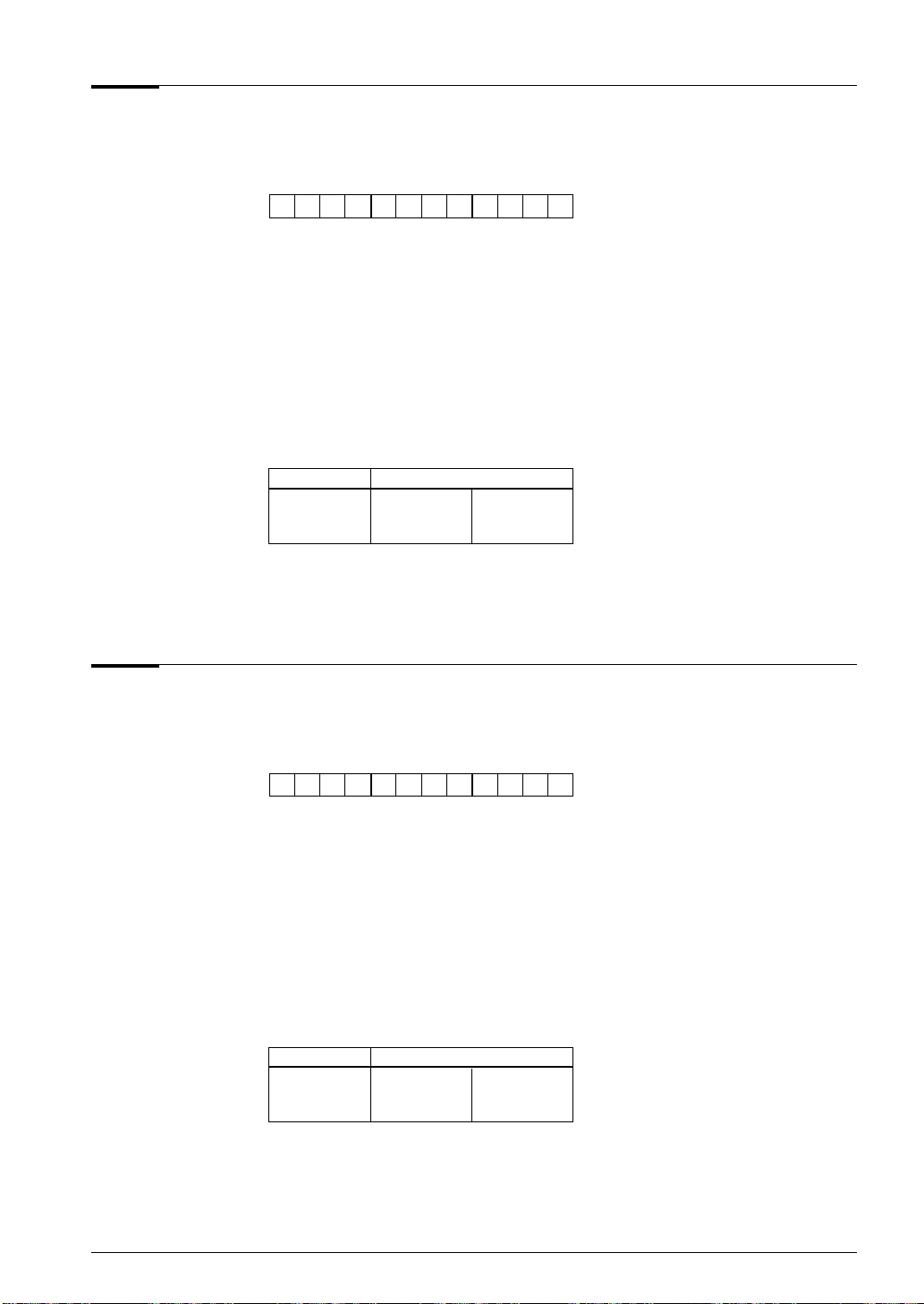
NOP5 No operation for 5 clock cycles
3 INSTRUCTION SET
Source Format:
Operation:
OP-Code:
Type:
Clock Cycles:
Flag:
Description:
Example:
NOP5
No operation (5 clock cycles)
11111111 1 011 FFBH
MSB LSB
VI
5
C –
Not affected
Z –
Not affected
D –
Not affected
I –
Not affected
Increments the program counter by 1. Has no other effect for 5 clock cycles.
NOP5
PCB 0 0
PCP 0011 0011
PCS 0001 0011 0001 0100
NOP7 No operation for 7 clock cycles
Source Format:
Operation:
OP-Code:
Type:
Clock Cycles:
Flag:
Description:
Example:
NOP7
No operation (7 clock cycles)
11111111 1 111 FFFH
MSB LSB
VI
7
C –
Not affected
Z –
Not affected
D –
Not affected
I –
Not affected
Increments the program counter by 1. Has no other effect for 7 clock cycles.
NOP7
PCB 0 0
PCP 1010 1010
PCS 1001 1001 1001 1010
S1C6200/6200A CORE CPU MANUAL EPSON 61
Page 68

3 INSTRUCTION SET
NOT r NOT r-register (one's complement)
Source Format:
Operation:
OP-Code:
Type:
Clock Cycles:
Flag:
Description:
Example:
NOT r
r ← r
110100r1 r0 1 1 1 1 D0FH to D3FH
MSB LSB
II
7
C –
Not affected
Z –
Set if the result is zero; otherwise, reset.
D –
Not affected
I –
Not affected
Performs a one's complement operation on the contents of the r-register.
NOT A NOT MY
A register 1001 0110 0110
Memory (MY) 1111 1111 0000
Z flag 0 0 1
OR r,i Logical OR immediate data i with r-register
Source Format:
Operation:
OP-Code:
Type:
Clock Cycles:
Flag:
Description:
Example:
OR r,i
r ← r ∨ i
3 to i0
110011r1 r0 i3 i2 i1 i0 CC0H to CFFH
MSB LSB
II
7
C –
Not affected
Z –
Set if the result is zero; otherwise, reset.
D –
Not affected
I –
Not affected
Performs a logical OR operation between immediate data i and the contents of the
r-register. The result is stored in the r-register.
OR B,5 OR MX,0BH
B register 0100 0101 0101
Memory (MX) 0011 0011 0111
Z flag 0 0 0
62 EPSON S1C6200/6200A CORE CPU MANUAL
Page 69

OR r,q Logical OR q-register with r-register
3 INSTRUCTION SET
Source Format:
Operation:
OP-Code:
Type:
Clock Cycles:
Flag:
Description:
Example:
OR r,q
r ← r ∨ q
10101101 r1 r0 q1 q0 AD0H to ADFH
MSB LSB
IV
7
C –
Not affected
Z –
Set if the result is zero; otherwise, reset.
D –
Not affected
I –
Not affected
Performs a logical OR operation between the contents of the q-register and the
contents of the r-register. The result is stored in the r-register.
OR MY,0 OR A,0CH
A register 0011 0011 1111
Memory (MY) 0000 0000 0000
Z flag 0 1 0
POP F Pop stack data into flags
Source Format:
Operation:
OP-Code:
Type:
Clock Cycles:
Flag:
Description:
Example:
POP F
F ← M(SP), SP ← SP + 1
11111101 1 010 FDAH
MSB LSB
VI
5
C –
Set or Reset by M(SP) data
Z –
Set or Reset by M(SP) data
D –
Set or Reset by M(SP) data
I –
Set or Reset by M(SP) data
Replaces the flags (F) with the contents of the data memory location addressed by
the stack pointer. SP is incremented by 1.
POP F
SP C0 C1
Memory (C0H) 1001 1001
Flags (I,D,Z,C) 0001 1001
M(SP) =
2322212
0
flag
C
flag
Z
flag
D
flag
I
S1C6200/6200A CORE CPU MANUAL EPSON 63
Page 70

3 INSTRUCTION SET
POP r Pop stack data into r-register
Source Format:
Operation:
OP-Code:
Type:
Clock Cycles:
Flag:
Description:
Example:
POP r
r ← M(SP), SP ← SP + 1
11111101 0 0r1 r0 FD0H to FD3H
MSB LSB
V
5
C –
Not affected
Z –
Not affected
D –
Not affected
I –
Not affected
Loads the contents of the data memory location addressed by the stack pointer
into the r-register. SP is incremented by 1.
POP B
SP C0 C1
Memory (C0H) 1001 1001
B register 0101 1001
M(SP) =
2322212
0
0
2
1
2
= r-register
2
2
3
2
POP XH Pop stack data into XH
Source Format:
Operation:
OP-Code:
Type:
Clock Cycles:
Flag:
Description:
Example:
POP XH
XH ← M(SP), SP ← SP + 1
11111101 0 101 FD5H
MSB LSB
VI
5
C –
Not affected
Z –
Not affected
D –
Not affected
I –
Not affected
Loads the contents of the data memory location addressed by the stack pointer
into XH, the four high-order bits of X. SP is incremented by 1.
POP XH
SP CE CF
Memory (CEH) 0110 0110
XH register 0010 0110
M(SP) =
2322212
0
0
2
1
2
= XH
2
2
3
2
64 EPSON S1C6200/6200A CORE CPU MANUAL
Page 71

POP XL Pop stack data into XL
3 INSTRUCTION SET
Source Format:
Operation:
OP-Code:
Type:
Clock Cycles:
Flag:
Description:
Example:
POP XL
XL ← M(SP), SP ← SP + 1
11111101 0 110 FD6H
MSB LSB
VI
5
C –
Not affected
Z –
Not affected
D –
Not affected
I –
Not affected
Loads the contents of the data memory location addressed by the stack pointer
into XL, the four low-order bits of X. SP is incremented by 1.
POP XL
SP C0 C1
Memory (C0H) 0001 0001
XL register 1101 0001
M(SP) =
2322212
0
0
2
1
2
= XL
2
2
3
2
POP XP Pop stack data into XP
Source Format:
Operation:
OP-Code:
Type:
Clock Cycles:
Flag:
Description:
Example:
POP XP
XP ← M(SP), SP ← SP + 1
11111101 0 100 FD4H
MSB LSB
VI
5
C –
Not affected
Z –
Not affected
D –
Not affected
I –
Not affected
Loads the contents of the data memory location addressed by the stack pointer
into XP, the 4-bit page part of IX. SP is incremented by 1.
POP XP
SP B4 B5
Memory (B4H) 0101 0101
XP register 0111 0101
M(SP) =
2322212
0
0
2
1
2
= XP
2
2
3
2
S1C6200/6200A CORE CPU MANUAL EPSON 65
Page 72

3 INSTRUCTION SET
POP YH Pop stack data into YH
Source Format:
Operation:
OP-Code:
Type:
Clock Cycles:
Flag:
Description:
Example:
POP YH
YH ← M(SP), SP ← SP + 1
11111101 1 000 FD8H
MSB LSB
VI
5
C –
Not affected
Z –
Not affected
D –
Not affected
I –
Not affected
Loads the contents of the data memory location addressed by the stack pointer
into YH, the four high-order bits of Y. SP is incremented by 1.
POP YH
SP C1 C2
Memory (C1H) 1101 1101
YH register 0010 1101
M(SP) =
2322212
0
0
2
1
2
= YH
2
2
3
2
POP YL Pop stack data into YL
Source Format:
Operation:
OP-Code:
Type:
Clock Cycles:
Flag:
Description:
Example:
POP YL
YL ← M(SP), SP ← SP + 1
11111101 1 001 FD9H
MSB LSB
VI
5
C –
Not affected
Z –
Not affected
D –
Not affected
I –
Not affected
Loads the contents of the data memory location addressed by the stack pointer
into YL, the four low-order bits of Y. SP is incremented by 1.
POP YL
SP CA CB
Memory (CAH) 0100 0100
YL register 0101 0100
M(SP) =
2322212
0
0
2
1
2
= YL
2
2
3
2
66 EPSON S1C6200/6200A CORE CPU MANUAL
Page 73

POP YP Pop stack data into YP
3 INSTRUCTION SET
Source Format:
Operation:
OP-Code:
Type:
Clock Cycles:
Flag:
Description:
Example:
POP YP
YP ← M(SP), SP ← SP + 1
11111101 0 111 FD7H
MSB LSB
VI
5
C –
Not affected
Z –
Not affected
D –
Not affected
I –
Not affected
Loads the contents of the data memory location addressed by the stack pointer
into YP, the 4-bit page part of IY. SP is incremented by 1.
POP YP
SP C0 C1
Memory (C0H) 0000 0000
YP register 0001 0000
M(SP) =
2322212
0
0
2
1
2
= YP
2
2
3
2
PSET p Page set
Source Format:
Operation:
OP-Code:
Type:
Clock Cycles:
Flag:
Description:
Example:
PSET p
NBP ← p
1110010p4 p3 p2 p1 p0 E40H to E5FH
MSB LSB
III
5
C –
Not affected
Z –
Not affected
D –
Not affected
I –
Not affected
Loads the most-significant bit of the 5-bit immediate data p to the new bank
pointer (NBP) and the four low-order bits to the new page pointer (NPP).
PCB 0 0 1
NBP 0 1 1
PCP 1000 1000 1111
NPP 0001 1111 1111
PCS 0010 0011 0010 0100 0000 0000
4, NPP ← p3 to p0
PSET 1FH JP 00H
S1C6200/6200A CORE CPU MANUAL EPSON 67
Page 74

3 INSTRUCTION SET
PUSH F Push flag onto stack
Source Format:
Operation:
OP-Code:
Type:
Clock Cycles:
Flag:
Description:
Example:
PUSH F
SP' ← SP - 1, M(SP') ← F
11111100 1 010 FCAH
MSB LSB
VI
5
C –
Not affected
Z –
Not affected
D –
Not affected
I –
Not affected
Decrements the stack pointer by 1 and loads the flags (F) into the data memory
location addressed by SP.
PUSH F
SP D0 CF
Memory (CFH) 0100 0001
Flags (I,D,Z,C) 0001 0001
M(SP) =
2322212
0
flag
C
flag
Z
flag
D
flag
I
PUSH r Push r-register onto stack
Source Format:
Operation:
OP-Code:
Type:
Clock Cycles:
Flag:
Description:
Example:
PUSH r
SP' ← SP - 1, M(SP') ← r
11111100 0 0r1 r0 FC0H to FC3H
MSB LSB
V
5
C –
Not affected
Z –
Not affected
D –
Not affected
I –
Not affected
Decrements the stack pointer by 1 and loads the contents of the r-register into the
data memory location addressed by SP.
PUSH A
SP D0 CF
Memory (CFH) 1000 0010
A register 0010 0010
M(SP) =
2322212
0
0
2
1
2
= r-register
2
2
3
2
68 EPSON S1C6200/6200A CORE CPU MANUAL
Page 75

PUSH XH Push XH onto stack
3 INSTRUCTION SET
Source Format:
Operation:
OP-Code:
Type:
Clock Cycles:
Flag:
Description:
Example:
PUSH XH
SP' ← SP - 1, M(SP') ← XH
11111100 0 101 FC5H
MSB LSB
VI
5
C –
Not affected
Z –
Not affected
D –
Not affected
I –
Not affected
Decrements the stack pointer by 1 and loads the contents of XH, the four highorder bits of XHL, into the data memory location addressed by SP.
PUSH XH
SP CC CB
Memory (CBH) 0000 1000
XH register 1000 1000
M(SP) =
2322212
0
0
2
1
2
= XH
2
2
3
2
PUSH XL Push XL onto stack
Source Format:
Operation:
OP-Code:
Type:
Clock Cycles:
Flag:
Description:
Example:
PUSH XL
SP' ← SP - 1, M(SP') ← XL
11111100 0 110 FC6H
MSB LSB
VI
5
C –
Not affected
Z –
Not affected
D –
Not affected
I –
Not affected
Decrements the stack pointer by 1 and loads the contents of XL, the four low-order
bits of XHL, into the data memory location addressed by SP.
SP D0 CF
Memory (CFH) 1111 0110
XL register 0110 0110
PUSH XL
M(SP) =
2322212
0
0
2
1
2
= XL
2
2
3
2
S1C6200/6200A CORE CPU MANUAL EPSON 69
Page 76
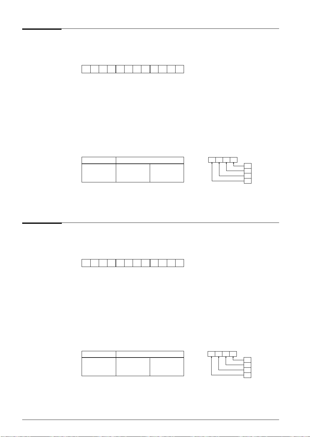
3 INSTRUCTION SET
PUSH XP Push XP onto stack
Source Format:
Operation:
OP-Code:
Type:
Clock Cycles:
Flag:
Description:
Example:
PUSH XP
SP' ← SP - 1, M(SP') ← XP
11111100 0 100 FC4H
MSB LSB
VI
5
C –
Not affected
Z –
Not affected
D –
Not affected
I –
Not affected
Decrements the stack pointer by 1 and loads the contents of XP, the page part of
IX, into the data memory location addressed by SP.
PUSH XP
SP D0 CF
Memory (CFH) 0011 0000
XP register 0000 0000
M(SP) =
2322212
0
0
2
1
2
= XP
2
2
3
2
PUSH YH Push YH onto stack
Source Format:
Operation:
OP-Code:
Type:
Clock Cycles:
Flag:
Description:
Example:
PUSH YH
SP' ← SP - 1, M(SP') ← YH
11111100 1 000 FC8H
MSB LSB
VI
5
C –
Not affected
Z –
Not affected
D –
Not affected
I –
Not affected
Decrements the stack pointer by 1 and loads the contents of YH, the four highorder bits of YHL, into the data memory location addressed by SP.
SP BF BE
Memory (BEH) 0100 0001
YH register 0001 0001
PUSH YH
M(SP) =
2322212
0
0
2
1
2
= YH
2
2
3
2
70 EPSON S1C6200/6200A CORE CPU MANUAL
Page 77

PUSH YL Push YL onto stack
3 INSTRUCTION SET
Source Format:
Operation:
OP-Code:
Type:
Clock Cycles:
Flag:
Description:
Example:
PUSH YL
SP' ← SP - 1, M(SP') ← YL
11111100 1 001 FC9H
MSB LSB
VI
5
C –
Not affected
Z –
Not affected
D –
Not affected
I –
Not affected
Decrements the stack pointer by 1 and loads the contents of YL, the four low-order
bits of YHL, into the data memory location addressed by SP.
PUSH YL
SP D0 CF
Memory (CFH) 0001 0111
YL register 0111 0111
M(SP) =
2322212
0
0
2
1
2
= YL
2
2
3
2
PUSH YP Push YP onto stack
Source Format:
Operation:
OP-Code:
Type:
Clock Cycles:
Flag:
Description:
Example:
PUSH YP
SP' ← SP - 1, M(SP') ← YP
11111100 0 111 FC7H
MSB LSB
VI
5
C –
Not affected
Z –
Not affected
D –
Not affected
I –
Not affected
Decrements the stack pointer by 1 and loads the contents of YP, the page part of
IY, into the data memory location addressed by SP.
SP C0 BF
Memory (BFH) 1111 0000
YP register 0000 0000
PUSH YP
M(SP) =
2322212
0
0
2
1
2
= YP
2
2
3
2
S1C6200/6200A CORE CPU MANUAL EPSON 71
Page 78

3 INSTRUCTION SET
RCF Reset carry flag
Source Format:
Operation:
OP-Code:
Type:
Clock Cycles:
Flag:
Description:
Example:
RCF
C ← 0
11110101 1 110 F5EH
MSB LSB
VI
7
C –
Reset
Z –
Not affected
D –
Not affected
I –
Not affected
Resets the C (carry) flag.
ADD A,4 RCF
A register 1101 0001 0001
C flag 0 1 0
RDF Reset decimal flag
Source Format:
Operation:
OP-Code:
Type:
Clock Cycles:
Flag:
Description:
Example:
RDF
D ← 0
11110101 1 011 F5BH
MSB LSB
VI
7
C –
Not affected
Z –
Not affected
D –
Reset
I –
Not affected
Resets the D (decimal) flag.
ADD A,8 RDF LD A,6 ADD A,8
A register 0110 0100 0100 0110 1110
D flag 11000
C flag 01110
Z flag 00000
72 EPSON S1C6200/6200A CORE CPU MANUAL
Page 79

RET Return from subroutine
3 INSTRUCTION SET
Source Format:
Operation:
OP-Code:
Type:
Clock Cycles:
Flag:
Description:
Example:
RET
PCSL ← M(SP), PCSH ← M(SP+1), PCP ← M(SP+2), SP ← SP + 3
11111101 1 111 FDFH
MSB LSB
VI
7
C –
Not affected
Z –
Not affected
D –
Not affected
I –
Not affected
Jumps to the return address that was pushed onto the stack when the subroutine
was called.
RET
PCP 1101 0010
PCS 1000 1101 0010 1101
SP BD C0
Memory (SP)
Memory (SP+1)
Memory (SP+2)
1101 1101
0010 0010
0010 0010
RETD e
Source Format:
Source Format:
Operation:
Operation:
Clock Cycles:
Clock Cycles:
Description:
Description:
OP-Code:
OP-Code:
Type:
Type:
Flag:
Flag:
Example:
Example:
Load immediate data e to memory, and increment X by 2, then return
RETD e
PCSL ← M(SP), PCSH ← M(SP+1), PCP ← M(SP+2), SP ← SP + 3,
M(X) ← e
MSB LSB
0001e
MSB LSB
I
12
C –
Z –
C –
D –
Z –
I –
D –
I –
Loads 8-bit immediate data e into the data memory location addressed by IX and
executes the RET command. X is incremented by 2.
PCP 0000 0010
PCS 1010 1011 0010 1101
SP BD C0
Memory (SP)
Memory (SP+1)
Memory (SP+2)
X register 0010 1010 0010 1100
Memory (2AH) 0000 0101
Memory (2BH) 0000 1111
3 to e0, M(X+1) ← e7 to e4, X ← X + 2
7 e6 e5 e4 e3 e2 e1 e0 100H to 1FFH
Not affected
Not affected
Not affected
Not affected
RETD F5H
1101 1101
0010 0010
0010 0010
S1C6200/6200A CORE CPU MANUAL EPSON 73
Page 80
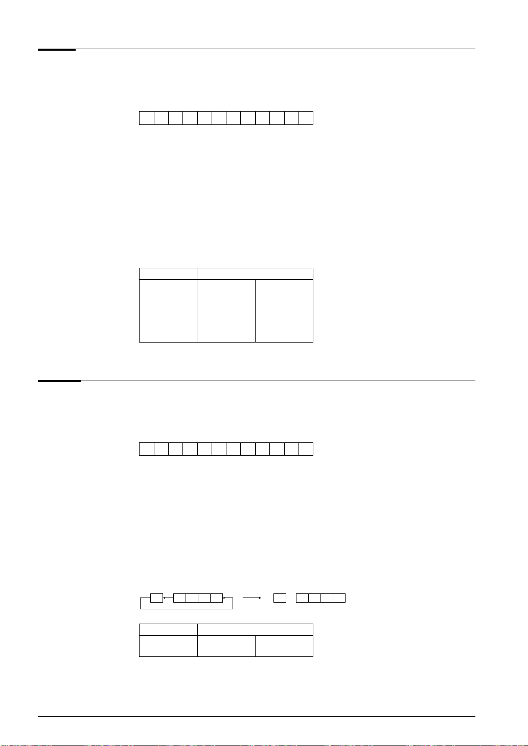
3 INSTRUCTION SET
RETS Return then skip an instruction
Source Format:
Operation:
OP-Code:
Type:
Clock Cycles:
Flag:
Description:
Example:
RETS
PCSL ← M(SP), PCSH ← M(SP+1), PCP ← M(SP+2), SP ← SP + 3, PC ← PC + 1
11111101 1 110 FDEH
MSB LSB
VI
12
C –
Not affected
Z –
Not affected
D –
Not affected
I –
Not affected
Jumps to the return address that was pushed onto the stack when the subroutine
was called and then skips one instruction.
RETS
PCP 0110 0000
PCS 1001 0000 0000 0111
SP B0 B3
Memory (SP)
Memory (SP+1)
Memory (SP+2)
0110 0110
0000 0000
0000 0000
RLC r Rotate r-register left with carry
Source Format:
Source Format:
Operation:
Operation:
OP-Code:
OP-Code:
Type:
Type:
Clock Cycles:
Clock Cycles:
Flag:
Flag:
Description:
Description:
Example:
Example:
RLC r
d
3 ← d2, d2 ← d1, d1 ← d0, d0 ← C, C ← d3
10101111 r1 r0 r1 r0 AF0H to AFFH
MSB LSB
IV
7
C –
Set when the high-order bit of the r-register is 1; otherwise, reset.
Z –
Not affected
D –
Not affected
I –
Not affected
Shifts the contents of the r-register one bit to the left. The high-order bit is shifted
into the carry flag and the carry bit becomes the low-order bit of the r-register.
r-register
C
C
d3 d2 d1 d0
C
d3
RLC A
A register 0011 0111
C flag 1 0
r-register
d
2 d1 d0
C
74 EPSON S1C6200/6200A CORE CPU MANUAL
Page 81
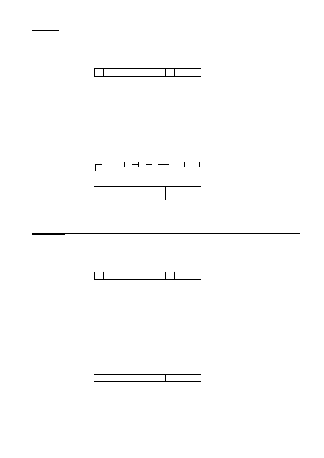
RRC r Rotate r-register right with carry
3 INSTRUCTION SET
Source Format:
Source Format:
Operation:
Operation:
OP-Code:
OP-Code:
Type:
Type:
Clock Cycles:
Clock Cycles:
Flag:
Flag:
Description:
Description:
Example:
Example:
RRC r
d
3 ← C, d2 ← d3, d1 ← d2, d0 ← d1, C ← d0
11101000 1 1r1 r0 E8CH to E8FH
MSB LSB
V
5
C –
Set when the low-order bit of the r-register is 1; otherwise, reset.
Z –
Not affected
D –
Not affected
I –
Not affected
Shifts the contents of the r-register one bit to the right. The low-order bit is shifted
into the carry flag and the carry bit becomes the high-order bit of the r-register.
r-registerCC
d3d2d1d
0
r-register
d
3d2d1
C
C
d
0
RRC MY
Memory (MY) 1010 1101
C flag 1 0
RST F,i Reset flags using immediate data i
Source Format:
Operation:
OP-Code:
Type:
Clock Cycles:
Flag:
Description:
Example:
RST F,i
F ← F ∧ i
3 to i0
11110101 i3 i2 i1 i0 F50H to F5FH
MSB LSB
IV
7
C –
Reset if i0 is zero; otherwise, not affected.
Z –
D –
I –
Reset if i
Reset if i
Reset if i
1 is zero; otherwise, not affected.
2 is zero; otherwise, not affected.
3 is zero; otherwise, not affected.
Performs a logical AND operation between immediate data i and the contents of
the flags. The result is stored in each respective flag.
RST F,2
Flags (I,D,Z,C) 1010 0010
S1C6200/6200A CORE CPU MANUAL EPSON 75
Page 82

3 INSTRUCTION SET
RZF Reset zero flag
Source Format:
Operation:
OP-Code:
Type:
Clock Cycles:
Flag:
Description:
Example:
RZF
Z ← 0
11110101 1 101 F5DH
MSB LSB
VI
7
C –
Not affected
Z –
Reset
D –
Not affected
I –
Not affected
Resets the Z (zero) flag.
ADD A,3 RZF
Z flag 0 1 0
A register 1101 0000 0000
SBC r,i Subtract with carry immediate data i from r-register
Source Format:
Operation:
OP-Code:
Type:
Clock Cycles:
Flag:
Description:
Example:
SBC r,i
r ← r - i
3 to i0 - C
110101r
MSB LSB
1 r0 i3 i2 i1 i0 D40H to D7FH
II
7
C –
Set if a borrow is generated; otherwise, reset.
Z –
Set if the result is zero; otherwise, reset.
D –
Not affected
I –
Not affected
Subtracts the carry flag and immediate data i from the r-register.
SBC A,9 SBC MY,0DH
A register 1000 1111 1111
Memory (MY) 1110 1110 0000
C flag 0 1 0
Z flag 0 0 1
76 EPSON S1C6200/6200A CORE CPU MANUAL
Page 83
SBC r,q Subtract with carry q-register from r-register
3 INSTRUCTION SET
Source Format:
Operation:
OP-Code:
Type:
Clock Cycles:
Flag:
Description:
Example:
SBC r,q
r ← r - q - C
10101011 r1 r0 q1 q0 AB0H to ABFH
MSB LSB
IV
7
C –
Set if a borrow is generated; otherwise, reset.
Z –
Set if the result is zero; otherwise, reset.
D –
Not affected
I –
Not affected
Subtracts the carry flag and the contents of the q-register from the r-register.
SBC A,B SBC MY,MX
A register 1110 1011 1011
B register 0010 0010 0010
Memory (MX) 1001 1001 1001
Memory (MY) 0100 0100 1011
C flag 1 0 1
Z flag 0 0 0
SCF Set carry flag
Source Format:
Operation:
OP-Code:
Type:
Clock Cycles:
Flag:
Description:
Example:
SCF
C ← 1
11110100 0 001 F41H
MSB LSB
VI
7
C –
Set
Z –
Not affected
D –
Not affected
I –
Not affected
Sets the C (carry) flag.
C flag 0 1
SCF
S1C6200/6200A CORE CPU MANUAL EPSON 77
Page 84

3 INSTRUCTION SET
SCPX MX,r Subtract with carry r-register from M(X) and increment X by 1
Source Format:
Operation:
OP-Code:
Type:
Clock Cycles:
Flag:
Description:
Example:
SCPX MX,r
M(X) ← M(X) - r - C, X ← X + 1
11110011 1 0r1 r0 F38H to F3BH
MSB LSB
V
7
C –
Set if a borrow is generated; otherwise, reset.
Z –
Set if the result is zero; otherwise, reset.
D –
Not affected
I –
Not affected
Subtracts the carry flag and the contents of the r-register from the data memory
location addressed by IX. X is incremented by 1. Incrementing X does not affect
the flags.
SCPX MX,B
X register 0101 0000 0101 0001
Memory (50H) 0110 0100
B register 0010 0010
C flag 0 0
Z flag 0 0
SCPY MY,r Subtract with carry r-register from M(Y) and increment Y by 1
Source Format:
Operation:
OP-Code:
Type:
Clock Cycles:
Flag:
Description:
Example:
SCPY MY,r
M(Y) ← M(Y) - r - C, Y ← Y + 1
11110011 1 1r1 r0 F3CH to F3FH
MSB LSB
V
7
C –
Set if a borrow is generated; otherwise, reset.
Z –
Set if the result is zero; otherwise, reset.
D –
Not affected
I –
Not affected
Subtracts the carry flag and the contents of the r-register from the data memory
location addressed by IY. Y is incremented by 1. Incrementing Y does not affect
the flags.
SCPY MY,A
Y register 1111 1111 0000 0000
Memory (FFH) 0111 0100
A register 0010 0010
C flag 1 0
Z flag 1 0
78 EPSON S1C6200/6200A CORE CPU MANUAL
Page 85

SDF Set decimal flag
3 INSTRUCTION SET
Source Format:
Operation:
OP-Code:
Type:
Clock Cycles:
Flag:
Description:
Example:
SDF
D ← 1
11110100 0 100 F44H
MSB LSB
VI
7
C –
Not affected
Z –
Not affected
D –
Set
I –
Not affected
Sets the D (decimal) flag.
SDF
D flag 0 1
SET F,i Set flags using immediate data i
Source Format:
Operation:
OP-Code:
Type:
Clock Cycles:
Flag:
Description:
Example:
SET F,i
F ← F ∨ i
3 to i0
11110100 i3 i2 i1 i0 F40H to F4FH
MSB LSB
IV
7
C –
Set if i0 is 1; otherwise, not affected.
Z –
Set if i
1 is 1; otherwise, not affected.
D –
Set if i
2 is 1; otherwise, not affected.
I –
Set if i
3 is 1; otherwise, not affected.
Performs a logical OR operation between immediate data i and the contents of the
flags. The results are stored in each respective flag.
SET F,0DH
Flags (C,Z,D,I) 0011 1111
S1C6200/6200A CORE CPU MANUAL EPSON 79
Page 86
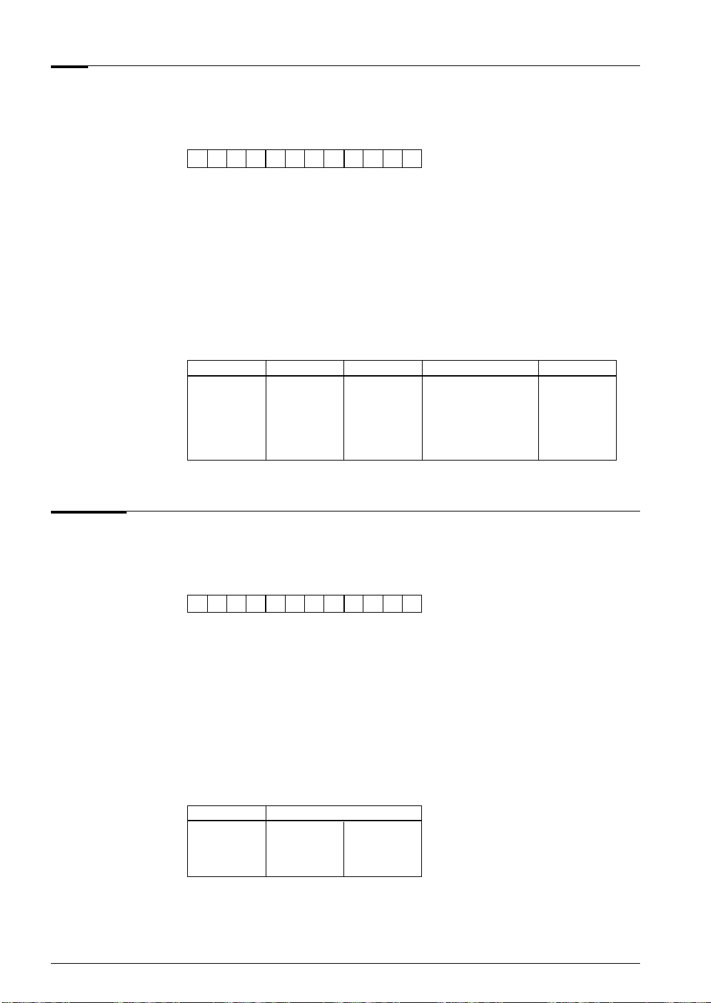
3 INSTRUCTION SET
SLP Sleep
Source Format:
Operation:
OP-Code:
Type:
Clock Cycles:
Flag:
Description:
Example:
SLP
Stop CPU and peripheral oscillator
11111111 1 001 FF9H
MSB LSB
VI
5
C –
Not affected
Z –
Not affected
D –
Not affected
I –
Not affected
Stops the CPU and the peripheral oscillator. When an interrupt occurs PCP and
PCS are pushed onto the stack as the return address and the interrupt service
routine is executed.
Instruction State PCP PCS I flag
RUN 0100 0011 0000 1
SLP 0100 0011 0001 1
Interrupt →
NOP5 RUN
SLEEP
0001 0000 0001 0
SUB r,q Subtract q-register from r-register
Source Format:
Operation:
OP-Code:
Type:
Clock Cycles:
Flag:
Description:
Example:
SUB r,q
r ← r - q
10101010 r1 r0 q1 q0 AA0H to AAFH
MSB LSB
IV
7
C –
Set if a borrow is generated; otherwise, reset.
Z –
Set if the result is zero; otherwise, reset.
D –
Not affected
I –
Not affected
Subtracts the contents of the q-register from the r-register.
SUB A,B
A register 1100 1001
B register 0011 0011
C flag 1 0
Z flag 0 0
80 EPSON S1C6200/6200A CORE CPU MANUAL
Page 87

SZF Set zero flag
3 INSTRUCTION SET
Source Format:
Operation:
OP-Code:
Type:
Clock Cycles:
Flag:
Description:
Example:
SZF
Z ← 1
11110100 0 010 F42H
MSB LSB
VI
7
C –
Not affected
Z –
Set
D –
Not affected
I –
Not affected
Sets the Z (zero) flag.
SZF
Z flag 0 1
XOR r,i Exclusive-OR immediate data i with r-register
Source Format:
Operation:
OP-Code:
Type:
Clock Cycles:
Flag:
Description:
Example:
XOR r,i
r ← r ∀ i
3 to i0
110100r1 r0 i3 i2 i1 i0 D00H to D3FH
MSB LSB
II
7
C –
Not affected
Z –
Set if the result is zero; otherwise, reset.
D –
Not affected
I –
Not affected
Performs an exclusive-OR operation between immediate data i and the contents
of the r-register. The result is stored in the r-register.
XOR A,12 XOR MX,1
A register 0110 1010 1010
Memory (MX) 0001 0001 0000
Z flag 0 0 1
S1C6200/6200A CORE CPU MANUAL EPSON 81
Page 88

3 INSTRUCTION SET
XOR r,q Exclusive-OR q-register with r-register
Source Format:
Operation:
OP-Code:
Type:
Clock Cycles:
Flag:
Description:
Example:
XOR r,q
r ← r ∀ q
1010111 0 r1 r0 q1 q0 AE0H to AEFH
MSB LSB
IV
7
C –
Not affected
Z –
Set if the result is zero; otherwise, reset.
D –
Not affected
I –
Not affected
Performs an exclusive-OR operation between the contents of the q-register and
the contents of the r-register. The result is stored in the r-register.
XOR A,MY XOR MX,B
A register 0100 1100 1100
B register 1111 1111 1111
Memory (MX) 0111 0111 1000
Memory (MY) 1000 1000 1000
Z flag 0 0 0
Source Format:
Operation:
OP-Code:
Type:
Clock Cycles:
Flag:
Description:
Example:
MSB LSB
C –
Z –
D –
I –
82 EPSON S1C6200/6200A CORE CPU MANUAL
Page 89

3 INSTRUCTION SET
ABBREVIATIONS
Source Format:
A............. A register (4 bits)
B............. B register (4 bits)
M(SP) ..... Contents of the data memory location whose address is specified by stack pointer SP (4 bits)
M(X) ....... Contents of the data memory location whose address is specified by IX (4 bits)
M(Y) ....... Contents of the data memory location whose address is specified by IY (4 bits)
M(n
MX.......... Data memory location whose address is specified by IX
MY.......... Data memory location whose address is specified by IY
NBP........ New Bank Pointer (1 bit)
NPP........ New Page Pointer (4 bits)
PCB........ Program Counter-Bank (1 bit)
PCP........ Program Counter-Page (4 bits)
PCS........ Program Counter-Step (8 bits)
PCSH ..... Four high-order bits of PCS
PCSL...... Four low-order bits of PCS
RP .......... Register Pointer (4 bits)
SP .......... Stack Pointer (8 bits)
SPH........ Four high-order bits of SP
SPL ........ Four low-order bits of SP
X............. Eight low-order bits of IX, that is, XHL
XH .......... Four high-order bits of X
XL........... Four low-order bits of X
XP .......... Four high-order bits of IX (page part)
Y............. Eight low-order bits of IY, that is, YHL
YH .......... Four high-order bits of Y
YL........... Four low-order bits of Y
YP .......... Four high-order bits of IY (page part)
+ ............. Addition
– ............. Subtraction
∧............... Logical AND
∨ ............. Logical OR
∀............. Exclusive-OR
↓ ............. Reset flag
↑ ............. Set flag
↕ ............. Set/reset flag
∗ ............. Decimal addition/subtraction
Operation:
OP-Code:
MSB LSB
3-0).... Contents of the data memory location within the register area 00H to 0FH (4 bits)
Type:
Clock Cycles:
Flag:
C –
Z –
D –
I –
Description:
Example:
Source Format:
Operation:
OP-Code:
MSB LSB
Type:
Clock Cycles:
Flag:
C –
Z –
D –
I –
Description:
Example:
S1C6200/6200A CORE CPU MANUAL EPSON 83
Page 90

APPENDIX A. S1C6200A (ADVANCED S1C6200) CORE CPU
APPENDIX A. S1C6200A (ADVANCED S1C6200) CORE CPU
S1C6200A is an improved version of the S1C6200. In this section, S1C6200A is described only in
terms of its differences with S1C6200. It is recommended that users of S1C6200A read this section.
S1C6200A is a Core CPU which has been made easier to integrate software by improving the parts of the
S1C6200 CPU which are difficult to use.
This section lists its differences with S1C6200; for items which are not included here, refer to the corresponding section in this manual.
A1 Outline of Differences
• The D (decimal) flag is set to "0" during initial reset.
• Modifications of the interrupt circuit
- The interrupt timing has been shifted to 0.5 clock later.
- <Reference> In the 1-chip micro controller which uses S1C6200A, writing on the interrupt mask register
and reading the interrupt factor flag during EI (enable interrupt flag) are possible. (However, consult
the respective hardware manuals to find out whether these are possible with the CPU peripheral
circuits.)
A2 Detailed Description of the Differences
A2.1 Initial reset
The D (decimal) flag will be set as follows through initial reset:
Table A2.1.1 D (decimal) flag initial setting
CPU Core
D (decimal) flag setting
S1C6200A
0
S1C6200
Undefined
Owing to this, bugs due to omission of D (decimal) flag setting during software development can now be
easily prevented.
For the values of other registers and flags during initial reset, see Section 2.5.4, "Initial reset".
A2.2 Interrupt
Operation during interrupt issuance
The time it takes to complete interrupt processing by hardware after the Core CPU receives the interrupt
request has changed as follows:
Table A2.2.1 Required interrupt processing time
Item
a) During instruction execution
b) At HALT mode
c) During PSET instruction execution
12-cycle instruction execution
7-cycle instruction execution
5-cycle instruction execution
PSET + CALL
PSET + JP
Figure A2.2.1 shows the timing chart of the S1C6200A interrupt.
S1C6200A
(clock cycles)
12.5 to 24.5
12.5 to 19.5
12.5 to 17.5
14 to 15
12.5 to 24.5
12.5 to 22.5
S1C6200
(clock cycles)
13 to 25
13 to 20
13 to 18
14 to 15
13 to 25
13 to 23
84 EPSON S1C6200/6200A CORE CPU MANUAL
Page 91

Clock
Status
APPENDIX A. S1C6200A (ADVANCED S1C6200) CORE CPU
Instruction
System clock
CPU clock
Status
Instruction
5-clock Instrruction
Status:
5-clock Instrruction
Status:
Fetch
Fetch
12-clock Instrruction
Interrupt
Interrupt processing:
Execute Note: (*1)
12-clock instruction
7-clock instruction
5-clock instruction
(*2)
a) During instruction execution
HALT
Execute Note: (*1)
(*2)
INT1 (*1) INT2 (*1) JP (*2)
... 12.5 to 24.5 clock cycles
... 12.5 to 19.5 clock cycles
... 12.5 to 17.5 clock cycles
INT1 and INT2 are dummy instructions
Branches to the top of the interrupt service routine
INT1 (*1) INT2 (*1) JP (*2)
Interrupt
Interrupt processing: 14 to 15 clock cycles
INT1 and INT2 are dummy instructions
Branches to the top of the interrupt service routine
Clock
Status
Instruction
Status:
PSET
Fetch
b) At HALT mode
CALL
Interrupt
Interrupt processing:
Execute Note: (*1)
INT1 (*1) INT2 (*1) JP (*2)
PSET + CALL
PSET + JP
... 12.5 to 24.5 clock cycles
... 12.5 to 22.5 clock cycles
INT1 and INT2 are dummy instructions
(*2)
Branches to the top of the interrupt service routine
c) During "PSET" instruction execution
Fig. A2.2.1 Timing chart of S1C6200A interrupt
S1C6200/6200A CORE CPU MANUAL EPSON 85
Page 92
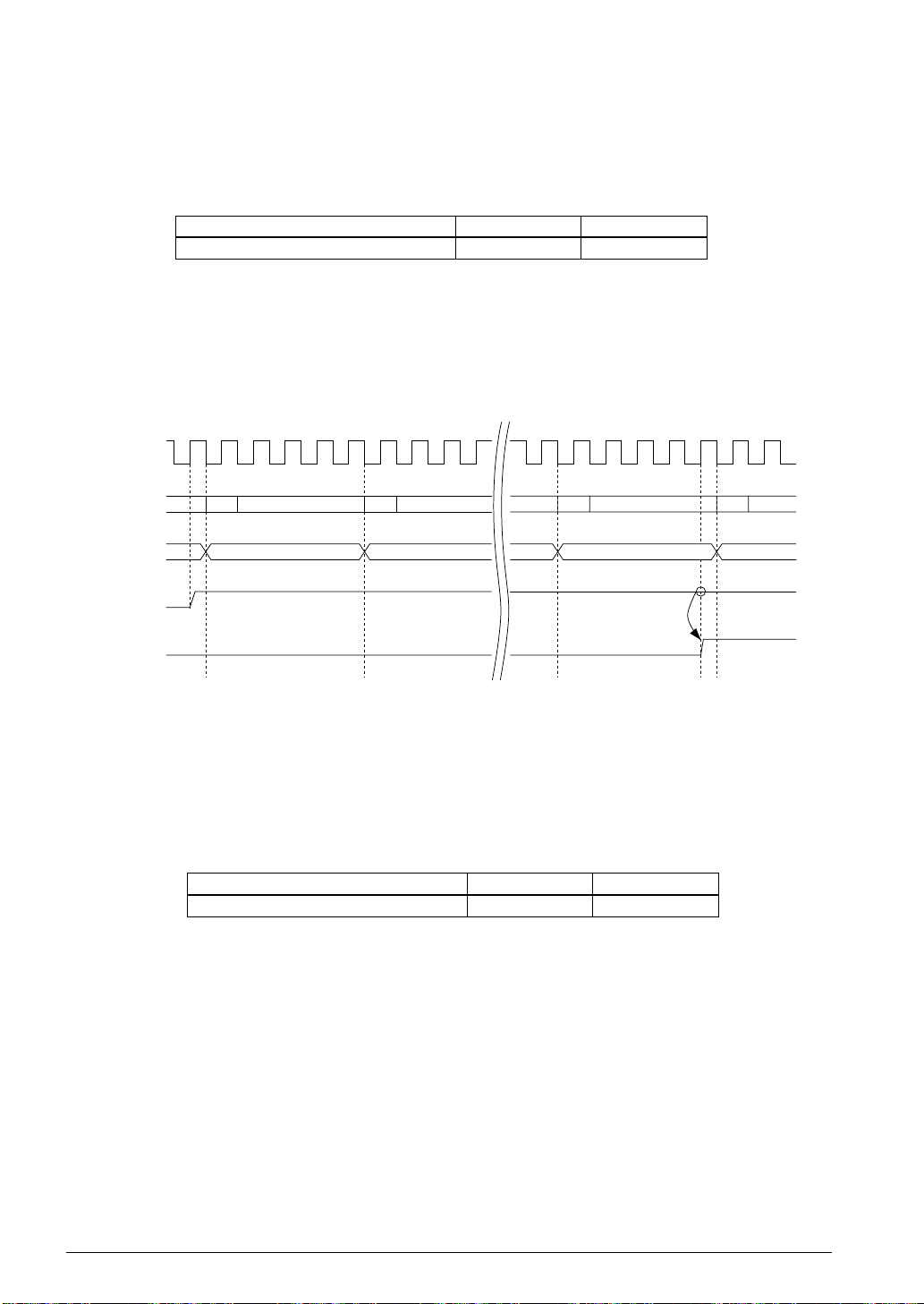
APPENDIX A. S1C6200A (ADVANCED S1C6200) CORE CPU
<Reference 1> Writing on the interrupt mask register during EI
This section describes the operation for writing on the interrupt mask register during EI (enable interrupt
flag) in the regular 1-chip micro controller which uses S1C6200 Core CPU and in the regular 1-chip micro
controller which uses S1C6200A Core CPU. For information on accurate operation, see the respective
hardware manuals of the S1C62 Family.
Table A2.2.2 Writing on the interrupt mask register at EI
CPU Core
Writing on the interrupt mask register at EI
S1C6200A
Possible
The operation during the instruction execution for writing "0" (i.e., to mask the interrupt factor) on the
interrupt mask register at EI is shown in Figure A2.2.2. At this point, the interrupt is masked 0.5 clock
before the start of the instruction execution through the 0.5 clock advance operation.
Moreover, during the instruction execution for writing "1" (i.e., to cancel the interrupt mask) on the mask
register at EI, it is the same as the ordinary interrupt timing as shown in Figure A2.2.2. In other words, if
the interrupt factor flag value is set to "1", the interrupt processing by hardware will start in the next
instruction execution cycle 0.5 clock before the completion of the instruction execution.
Clock
S1C6200
Not possible
Status
Instruction
Corresponding
interrupt factor flag
Interrupt request
Fetch Execute Fetch Execute Fetch Execute Fetch
"0" is written to the interrupt mask register
Execute next instruction INT1(interrupt processing)
"1" is written to the interrupt mask register
Fig. A2.2.2 Writing on the interrupt mask register and interrupt request generation
<Reference 2> Reading the interrupt factor flag during EI
This section describes the operation for reading the interrupt factor flag during EI (enable interrupt flag) in
the regular 1-chip micro controller which uses S1C6200 Core CPU and in the regular 1-chip micro controller which uses S1C6200A Core CPU. For information on accurate operation, see the respective hardware
manuals of the S1C62 Family.
Table A2.2.3 Reading the interrupt factor flag at EI
CPU Core
Reading the interrupt factor flag at EI
S1C6200A
Possible
At EI, reading the interrupt factor flag is possible but caution must be observed in the following case: when
the value of the interrupt mask register corresponding to the interrupt factor flag which is to be read is set
to "1" (unmasked). In this case, interrupt request may be issued to the CPU due to the timing by which the
interrupt factor flag is set to "1", or the interrupt factor flag may be cleared by reading it and hence interrupt request will not be issued.
Particularly when there are multiple interrupt factor flags in the same address, extra caution is required.
S1C6200
Not possible
86 EPSON S1C6200/6200A CORE CPU MANUAL
Page 93

APPENDIX B. INSTRUCTION INDEX
ACPX MX,r Add with carry r-register to M(X), increment X by 1 ...........................28
A
ACPY MY,r Add with carry r-register to M(Y), increment Y by 1 ........................... 28
ADC r,i Add with carry immediate data i to r-register...................................... 29
ADC r,q Add with carry q-register to r-register.................................................29
ADC XH,i Add with carry immediate data i to XH................................................30
ADC XL,i Add with carry immediate data i to XL ................................................30
ADC YH,i Add with carry immediate data i to YH ................................................ 31
ADC YL,i Add with carry immediate data i to YL ................................................ 31
ADD r,i Add immediate data i to r-register .......................................................32
ADD r,q Add q-register to r-register ..................................................................32
AND r,i Logical AND immediate data i with r-register..................................... 33
AND r,q Logical AND q-register with r-register ................................................33
CALL s Call subroutine .....................................................................................34
C
CALZ s Call subroutine at page zero ................................................................ 34
CP r,i Compare immediate data i with r-register ........................................... 35
CP r,q Compare q-register with r-register ......................................................35
CP XH,i Compare immediate data i with XH .....................................................36
CP XL,i Compare immediate data i with XL......................................................36
CP YH,i Compare immediate data i with YH .....................................................37
CP YL,i Compare immediate data i with YL...................................................... 37
APPENDIX B. INSTRUCTION INDEX
DEC Mn Decrement memory ..............................................................................38
D
DEC SP Decrement stack pointer.......................................................................38
DI Disable interrupts................................................................................. 39
EI Enable interrupts .................................................................................. 39
E
FAN r,i Logical AND immediate data i with r-register for flag check.............. 40
F
FAN r,q Logical AND q-register with r-register for flag check.........................40
HALT Halt ....................................................................................................... 41
H
INC Mn Increment memory by 1 ........................................................................ 41
I
INC SP Increment stack pointer by 1 ................................................................ 42
INC X Increment X-register by 1.....................................................................42
INC Y Increment Y-register by 1 .....................................................................43
JPBA Indirect jump using registers A and B..................................................43
J
JP C,s Jump if carry flag is set ........................................................................44
JP NC,s Jump if not carry ..................................................................................44
JP NZ,s Jump if not zero ....................................................................................45
JP s Jump .....................................................................................................45
JP Z,s Jump if zero .......................................................................................... 46
S1C6200/6200A CORE CPU MANUAL EPSON 87
Page 94

APPENDIX B. INSTRUCTION INDEX
LBPX MX,e Load immediate data e to memory, and increment X by 2 ................... 46
L
LD A,Mn Load memory into A-register ............................................................... 47
LD B,Mn Load memory into B-register ............................................................... 47
LD Mn,A Load A-register into memory ............................................................... 48
LD Mn,B Load B-register into memory ............................................................... 48
LDPX MX,i Load immediate data i into MX, increment X by 1...............................49
LDPX r,q Load q-register into r-register, increment X by 1 ................................49
LDPY MY,i Load immediate data i into MY, increment Y by 1 ............................... 50
LDPY r,q Load q-register into r-register, increment Y by 1 ................................ 50
LD r,i Load immediate data i into r-register ..................................................51
LD r,q Load q-register into r-register ............................................................. 51
LD r,SPH Load SPH into r-register ......................................................................52
LD r,SPL Load SPL into r-register ......................................................................52
LD r,XH Load XH into r-register ........................................................................53
LD r,XL Load XL into r-register ........................................................................ 53
LD r,XP Load XP into r-register ........................................................................54
LD r,YH Load YH into r-register ........................................................................ 54
LD r,YL Load YL into r-register.........................................................................55
LD r,YP Load YP into r-register ........................................................................55
LD SPH,r Load r-register into SPH ......................................................................56
LD SPL,r Load r-register into SPL ......................................................................56
LD X,e Load immediate data e into X-register................................................. 57
LD XH,r Load r-register into XH ........................................................................57
LD XL,r Load r-register into XL ........................................................................ 58
LD XP,r Load r-register into XP ........................................................................58
LD Y,e Load immediate data e into Y-register .................................................59
LD YH,r Load r-register into YH ........................................................................ 59
LD YL,r Load r-register into YL.........................................................................60
LD YP,r Load r-register into YP ........................................................................60
NOP5 No operation for 5 clock cycles............................................................61
N
NOP7 No operation for 7 clock cycles............................................................61
NOT r NOT r-register (one's complement)......................................................62
OR r,i Logical OR immediate data i with r-register ....................................... 62
O
OR r,q Logical OR q-register with r-register ..................................................63
POP F Pop stack data into flags ...................................................................... 63
P
POP r Pop stack data into r-register...............................................................64
POP XH Pop stack data into XH.........................................................................64
POP XL Pop stack data into XL .........................................................................65
POP XP Pop stack data into XP ......................................................................... 65
POP YH Pop stack data into YH......................................................................... 66
POP YL Pop stack data into YL ......................................................................... 66
POP YP Pop stack data into YP .........................................................................67
PSET p Page set ................................................................................................67
PUSH F Push flag onto stack .............................................................................68
88 EPSON S1C6200/6200A CORE CPU MANUAL
Page 95

APPENDIX B. INSTRUCTION INDEX
PUSH r Push r-register onto stack ....................................................................68
P
PUSH XH Push XH onto stack ..............................................................................69
PUSH XL Push XL onto stack ...............................................................................69
PUSH XP Push XP onto stack............................................................................... 70
PUSH YH Push YH onto stack ..............................................................................70
PUSH YL Push YL onto stack ............................................................................... 71
PUSH YP Push YP onto stack ...............................................................................71
RCF Reset carry flag .................................................................................... 72
R
RDF Reset decimal flag ................................................................................72
RET Return from subroutine ........................................................................73
RETD e Load immediate data e to memory, and increment X by 2, then return73
RETS Return then skip an instruction ............................................................74
RLC r Rotate r-register left with carry ...........................................................74
RRC r Rotate r-register right with carry .........................................................75
RST F,i Reset flags using immediate data i....................................................... 75
RZF Reset zero flag ......................................................................................76
SBC r,i Subtract with carry immediate data i from r-register .......................... 76
S
SBC r,q Subtract with carry q-register from r-register .....................................77
SCF Set carry flag ........................................................................................77
SCPX MX,r Subtract with carry r-register from M(X) and increment X by 1 .........78
SCPY MY,r Subtract with carry r-register from M(Y) and increment Y by 1.......... 78
SDF Set decimal flag ....................................................................................79
SET F,i Set flags using immediate data i...........................................................79
SLP Sleep ..................................................................................................... 80
SUB r,q Subtract q-register from r-register.......................................................80
SZF Set zero flag ..........................................................................................81
XOR r,i Exclusive-OR immediate data i with r-register ....................................81
X
XOR r,q Exclusive-OR q-register with r-register ............................................... 82
S1C6200/6200A CORE CPU MANUAL EPSON 89
Page 96

International Sales Operations
AMERICA
EPSON ELECTRONICS AMERICA, INC.
- HEADQUARTERS -
1960 E. Grand Avenue
EI Segundo, CA 90245, U.S.A.
Phone: +1-310-955-5300 Fax: +1-310-955-5400
- SALES OFFICES West
150 River Oaks Parkway
San Jose, CA 95134, U.S.A.
Phone: +1-408-922-0200 Fax: +1-408-922-0238
Central
101 Virginia Street, Suite 290
Crystal Lake, IL 60014, U.S.A.
Phone: +1-815-455-7630 Fax: +1-815-455-7633
Northeast
301 Edgewater Place, Suite 120
Wakefield, MA 01880, U.S.A.
Phone: +1-781-246-3600 Fax: +1-781-246-5443
Southeast
3010 Royal Blvd. South, Suite 170
Alpharetta, GA 30005, U.S.A.
Phone: +1-877-EEA-0020 Fax: +1-770-777-2637
EUROPE
EPSON EUROPE ELECTRONICS GmbH
- HEADQUARTERS -
Riesstrasse 15
80992 Munich, GERMANY
Phone: +49-(0)89-14005-0 Fax: +49-(0)89-14005-110
ASIA
EPSON (CHINA) CO., LTD.
28F, Beijing Silver Tower 2# North RD DongSanHuan
ChaoYang District, Beijing, CHINA
Phone: 64106655 Fax: 64107319
SHANGHAI BRANCH
4F, Bldg., 27, No. 69, Gui Jing Road
Caohejing, Shanghai, CHINA
Phone: 21-6485-5552 Fax: 21-6485-0775
EPSON HONG KONG LTD.
20/F., Harbour Centre, 25 Harbour Road
Wanchai, Hong Kong
Phone: +852-2585-4600 Fax: +852-2827-4346
Telex: 65542 EPSCO HX
EPSON TAIWAN TECHNOLOGY & TRADING LTD.
10F, No. 287, Nanking East Road, Sec. 3
Taipei
Phone: 02-2717-7360 Fax: 02-2712-9164
Telex: 24444 EPSONTB
HSINCHU OFFICE
13F-3, No. 295, Kuang-Fu Road, Sec. 2
HsinChu 300
Phone: 03-573-9900 Fax: 03-573-9169
EPSON SINGAPORE PTE., LTD.
No. 1 Temasek Avenue, #36-00
Millenia Tower, SINGAPORE 039192
Phone: +65-337-7911 Fax: +65-334-2716
SEIKO EPSON CORPORATION KOREA OFFICE
50F, KLI 63 Bldg., 60 Yoido-dong
Youngdeungpo-Ku, Seoul, 150-763, KOREA
Phone: 02-784-6027 Fax: 02-767-3677
SALES OFFICE
Altstadtstrasse 176
51379 Leverkusen, GERMANY
Phone: +49-(0)2171-5045-0 Fax: +49-(0)2171-5045-10
UK BRANCH OFFICE
Unit 2.4, Doncastle House, Doncastle Road
Bracknell, Berkshire RG12 8PE, ENGLAND
Phone: +44-(0)1344-381700 Fax: +44-(0)1344-381701
FRENCH BRANCH OFFICE
1 Avenue de l' Atlantique, LP 915 Les Conquerants
Z.A. de Courtaboeuf 2, F-91976 Les Ulis Cedex, FRANCE
Phone: +33-(0)1-64862350 Fax: +33-(0)1-64862355
BARCELONA BRANCH OFFICE
Barcelona Design Center
Edificio Prima Sant Cugat
Avda. Alcalde Barrils num. 64-68
E-08190 Sant Cugat del Vallès, SPAIN
Phone: +34-93-544-2490 Fax: +34-93-544-2491
SEIKO EPSON CORPORATION
ELECTRONIC DEVICES MARKETING DIVISION
Electronic Device Marketing Department
IC Marketing & Engineering Group
421-8, Hino, Hino-shi, Tokyo 191-8501, JAPAN
Phone: +81-(0)42-587-5816 Fax: +81-(0)42-587-5624
ED International Marketing Department Europe & U.S.A.
421-8, Hino, Hino-shi, Tokyo 191-8501, JAPAN
Phone: +81-(0)42-587-5812 Fax: +81-(0)42-587-5564
ED International Marketing Department Asia
421-8, Hino, Hino-shi, Tokyo 191-8501, JAPAN
Phone: +81-(0)42-587-5814 Fax: +81-(0)42-587-5110
Page 97

In pursuit of “Saving” Tec hnology, Epson electronic devices.
Our lineup of semiconductors, liquid crystal displays and quartz devices
assists in creating the products of our customers’ dreams.
Epson IS energy savings.
Page 98

S1C6200/6200A
Core CPU Manual
ELECTRONIC DEVICES MARKETING DIVISION
EPSON Electronic Devices Website
http://www.epson.co.jp/device/
First issue February, 1989
Printed February, 2001 in Japan A
M
 Loading...