

Page 1
MF1517-01
CMOS 32-BIT SINGLE CHIP MICROCOMPUTER
S1C33210
Technical Manual
S1C33210 PRODUCT PART
S1C33210 FUNCTION PART
Page 2

NOTICE
No part of this material may be reproduced or duplicated in any form or by any means without the written
permission of Seiko Epson. Seiko Epson reserves the right to make changes to this material without notice.
Seiko Epson does not assume any liability of any kind arising out of any inaccuracies contained in this material
or due to its application or use in any product or circuit and, further, there is no representation that this material
is applicable to products requiring high level reliability, such as medical products. Moreover, no license to any
intellectual property rights is granted by implication or otherwise, and there is no representation or warranty that
anything made in accordance with this material will be free from any patent or copyright infringement of a third
party. This material or portions thereof may contain technology or the subject relating to strategic products under
the control of the Foreign Exchange and Foreign Trade Law of Japan and may require an export license from
the Ministry of International Trade and Industry or other approval from another government agency.
2002 All rights reserved.
Page 3
S1C33210 Technical Manual
This manual describes the hardware specifications of the Seiko Epson original 32-bit microcomputer S1C33210.
S1C33210 PRODUCT PART
Describes the hardware specifications of the S1C33210 except for details of the peripheral circuits.
S1C33210 FUNCTION PART
Describes details of all the peripheral circuit blocks for the S1C33 Family microcomputers.
R e f e r t o t he " S 1C 33 000 C or e C P U M a nua l " f or de t a i l s of t he S 1C 330 00 32- bi t R I S C C P U .
New configuration of product number
Starting April 1, 2001, the configuration of product number descriptions will be changed as listed
below. To order from April 1, 2001 please use these product numbers. For further information, please
contact Epson sales representative.
Devices
S1
C 33104 F 0A01
Development tools
S5U1
C 33L01 D1 1
00
Packing specification
Specification
Package (D: die form; F: QFP)
Model number
Model name (C: microcomputer, digital products)
Product classification (S1: semiconductor)
00
Packing specification
Version (1: Version 1)
Tool type (D1: Development Tool)
Corresponding model number (33L01: for S1C33L01)
Tool classification (C: microcomputer use)
Product classification
(S5U1: development tool for semiconductor products)
Page 4

Page 5

TABLE OF CONTENTS
S1C33210 PRODUCT PART
Table of Contents
1 Outline.....................................................................................................................A-1
1.1 Features...............................................................................................................................................................A-1
1. 2 Bl o c k D iag r a m ...................................................................................................................................................A-3
1.3 Pin Description ..................................................................................................................................................A-4
1.3.1 Pin Layout Diagram (plastic package)...................................................................................A-4
1. 3 . 2 P i n F u nct i o n s ...................................................................................................................................A-5
2 Power Supply ........................................................................................................ A-11
2.1 Power Supply Pins.........................................................................................................................................A-11
2.2 Operating Voltage (V
2.3 Power Supply for Analog Circuits (AV
3 Internal Memory....................................................................................................A-13
3.1 ROM and Boot Address...............................................................................................................................A-13
3.2 RAM.....................................................................................................................................................................A-13
4 Peripheral Circuits................................................................................................A-14
4.1 List of Peripheral Circuits............................................................................................................................A-14
4.2 I/O Memory Map.............................................................................................................................................A-15
DD, VSS)....................................................................................................................A-11
DD)..............................................................................................A-12
5 Po we r -D o w n C o n tr o l.............................................................................................A-62
6 Ba si c E xt er na l Wi ri ng Diagr am..............................................................................A-65
7 Precautions on Mounting......................................................................................A-66
8 El ec t r i c a l C h a r a c t e r i s t i c s......................................................................................A-6 8
8.1 Absolute Maximum Rating..........................................................................................................................A-68
8.2 Recommended Operating Conditions ....................................................................................................A-69
8.3 DC Characteristics..........................................................................................................................................A-70
8.4 Current Consumption....................................................................................................................................A-71
8.5 A/D Converter Characteristics...................................................................................................................A-72
8.6 AC Characteristics..........................................................................................................................................A-74
8.6.1 Symbol Description.....................................................................................................................A-74
8.6.2 AC Characteristics Measurement Condition......................................................................A-74
8.6.3 C3 3 Block AC Characteristic Tables....................................................................................A-75
8.6.4 C33 Block AC Characteristic Timing Charts.......................................................................A-78
8.7 Oscillation Characteristics...........................................................................................................................A-85
8.8 PLL Characteristics........................................................................................................................................A-86
9 Package ................................................................................................................ A-87
9.1 Plastic Package...............................................................................................................................................A-87
10 Pad Layout............................................................................................................A-88
10.1 Pad Layout Diagram.....................................................................................................................................A-88
10.2 Pad Co ordinate ...............................................................................................................................................A-89
EPSON i
Page 6

TABLE OF CONTENTS
Appendix A <Reference> External Device Interface Timings......................................A-92
A.1 DRAM (70ns)....................................................................................................................................................A-93
A.2 DRAM (60ns)....................................................................................................................................................A-96
A.3 ROM and Burst ROM.................................................................................................................................A-100
A.4 SRAM (55ns).................................................................................................................................................A-102
A.5 SRAM (70ns).................................................................................................................................................A-104
A.6 8255A...............................................................................................................................................................A-106
Appendix B Pin Characteristics................................................................................A-107
ii EPSON
Page 7

TABLE OF CONTENTS
S1C33210 FUNCTION PART
Table of Contents
I OUTLINE
I-1 INTRODUCTION............................................................................................... B-I-1-1
I-2 BLOCK DIAGRAM............................................................................................ B-I-2-1
I-3 LIST O F PINS................................................................................................... B-I-3-1
List of External I/O Pins.....................................................................................................................................B-I-3-1
II CORE BLOCK
II-1 INTRODUCTION.............................................................................................. B-II-1-1
II-2 CPU AND OPERATING MODE......................................................................... B-II-2-1
CPU.........................................................................................................................................................................B-II-2-1
Standby Mode.....................................................................................................................................................B-II-2-2
HALT Mode............................................................................................................................................B-II-2-2
SLEEP Mode.........................................................................................................................................B-II-2-2
Notes on Standby Mode...................................................................................................................B-II-2-3
Test Mode.............................................................................................................................................................B-II-2-3
Debug Mode.........................................................................................................................................................B-II-2-3
Trap Table.............................................................................................................................................................B-II-2-4
II-3 INITIAL RESET ................................................................................................ B-II-3-1
Pins for Initial Reset...........................................................................................................................................B-II-3-1
Cold Start and Hot Start..................................................................................................................................B-II-3-1
Power-on Reset..................................................................................................................................................B-II-3-2
Reset Pulse ..........................................................................................................................................................B-II-3-2
Boot Address........................................................................................................................................................B-II-3-3
Notes Related to Initial Reset........................................................................................................................B-II-3-3
II-4 BCU (BUS CONTROL UNIT) ............................................................................B-II-4-1
Pin Assignment for External System Interface.......................................................................................B-II-4-1
I/ O P i n L i s t ..............................................................................................................................................B-II-4-1
Combination of System Bus Control Signals............................................................................B-II-4-3
Memory Area........................................................................................................................................................B-II-4-4
Memory Map..........................................................................................................................................B-II-4-4
External Memory Map and Chip Enable .....................................................................................B-II-4-5
Using Internal Memory on External Memory Area..................................................................B-II-4-7
Exclusive Signals for Areas .............................................................................................................B-II-4-7
Ar e a 1 0 ....................................................................................................................................................B-II-4-8
Ar e a 3 ......................................................................................................................................................B-II-4-8
Setting External Bus Conditions...................................................................................................................B-II-4-9
Setting Device Type and Size ........................................................................................................B-II-4-9
Setting SRAM Timing Conditions.................................................................................................B-II-4-10
Setting Timing Conditions of Burst ROM ..................................................................................B-II-4-11
Bus Operation....................................................................................................................................................B-II-4-12
Data Arrangement in Memory.......................................................................................................B-II-4-12
Bus Operation of External Memory.............................................................................................B-II-4-12
Bus Clock.............................................................................................................................................................B-II-4-16
EPSON iii
Page 8

TABLE OF CONTENTS
Bus Speed Mode ...............................................................................................................................B-II-4-17
Bus Clock Output...............................................................................................................................B-II-4-17
Bus Cycles in External System Interface................................................................................................B-II-4-18
SRAM Read Cycles...........................................................................................................................B-II-4-18
Bus Timing............................................................................................................................................B-II-4-19
SRAM Write Cycles...........................................................................................................................B-II-4-20
Burst ROM Read Cycles .................................................................................................................B-II-4-22
DRAM Direct Interface....................................................................................................................................B-II-4-23
Outline of DRAM Interface .............................................................................................................B-II-4-23
DRAM Setting Conditions...............................................................................................................B-II-4-24
DRAM Read/Write Cycles...............................................................................................................B-II-4-27
DRAM Refresh Cycles.....................................................................................................................B-II-4-30
Re l e a s ing E x t ern a l Bus .................................................................................................................................B-II-4-31
Power-down Control by External Device ................................................................................................B-II-4-32
I/O Memory of BCU.........................................................................................................................................B-II-4-33
II-5 ITC (Interrupt Controller).................................................................................B-II-5-1
Outline of Interrupt Functions.........................................................................................................................B-II-5-1
Maskable Interrupts.............................................................................................................................B-II-5-1
Interrupt Factors and Intelligent DMA...........................................................................................B-II-5-3
Nonmaskable Interrupt (NMI)..........................................................................................................B-II-5-3
Interrupt Processing by the CPU....................................................................................................B-II-5-3
Clearing Standby Mode by Interrupts...........................................................................................B-II-5-3
Trap Table.............................................................................................................................................................B-II-5-4
Control of Maskable Interrupts......................................................................................................................B-II-5-5
Structure of the Interrupt Controller...............................................................................................B-II-5-5
Processor Status Register (PSR)...................................................................................................B-II-5-5
Interrupt Factor Flag and Interrupt Enable Register...............................................................B-II-5-6
Interrupt Priority Register and Interrupt Levels.........................................................................B-II-5-8
IDMA Invocation..................................................................................................................................................B-II-5-9
HSDMA Invocation...........................................................................................................................................B-II-5-11
I/O Memory of Interrupt Controller .............................................................................................................B-II-5-12
Programming Notes.........................................................................................................................................B-II-5-25
II-6 CLG (Clock Generator)....................................................................................B-II-6-1
Configuration of Clock Generator.................................................................................................................B-II-6-1
I/O Pins of Clock Generator...........................................................................................................................B-II-6-2
High-Speed (OSC3) Oscillation Circuit.......................................................................................................B-II-6-2
PLL .........................................................................................................................................................................B-II-6-3
Controlling Oscillation.......................................................................................................................................B-II-6-3
Setting and Switching Over the CPU Operating Clock.........................................................................B-II-6-4
Power-Control Register Protection Flag....................................................................................................B-II-6-5
Operation in Standby Mode...........................................................................................................................B-II-6-5
I/O Memory of Clock Generator....................................................................................................................B-II-6-6
Programming Notes...........................................................................................................................................B-II-6-9
II-7 DBG (Debug Unit)............................................................................................B-II-7-1
Debug Circuit........................................................................................................................................................B-II-7-1
I/O Pins of Debug Circuit.................................................................................................................................B-II-7-1
iv EPSON
Page 9

TABLE OF CONTENTS
III PERIPHERAL BLOCK
III-1 INTRODUCTION ............................................................................................ B-III-1-1
III-2 PRESCALER.................................................................................................B-III-2-1
Configuration of Prescaler..............................................................................................................................B-III-2-1
Source Clock.......................................................................................................................................................B-III-2-1
Selecting Division Ratio and Output Control for Prescaler...............................................................B-III-2-2
Source Clock Output to 8-Bit Programmable Timer.............................................................................B-III-2-2
I/O Memory of Prescaler.................................................................................................................................B-III-2-3
Programming Notes..........................................................................................................................................B-III-2-7
III-3 8-BIT PROGRAMMABLE TIMERS .................................................................B-III-3-1
Configuration of 8-Bit Programmable Timer............................................................................................B-III-3-1
Output Pins of 8-Bit Programmable Timers.............................................................................................B-III-3-1
Uses of 8-Bit Programmable Timers...........................................................................................................B-III-3-2
Control and Operation of 8-Bit Programmable Timer ..........................................................................B-III-3-4
Co n t r o l o f Clo c k Ou tpu t ...................................................................................................................................B-III-3-7
8-Bit Programmable Timer Interrupts and DMA.....................................................................................B-III-3-8
I/O Memory of 8-Bit Programmable Timers...........................................................................................B-III-3-10
Programming Notes........................................................................................................................................B-III-3-17
III-4 16-BIT PROGRAMMABLE TIMERS................................................................ B-III-4-1
Configuration of 16-Bit Programmable Timer..........................................................................................B-III-4-1
I/O Pins of 16-Bit Programmable Timers..................................................................................................B-III-4-2
Uses of 16-Bit Programmable Timers........................................................................................................B-III-4-3
Control and Operation of 16-Bit Programmable Timer........................................................................B-III-4-4
Co n t r o lli n g C loc k Ou tpu t .................................................................................................................................B-III-4-7
16-Bit Programmable Timer Interrupts and DMA..................................................................................B-III-4-9
I/O Memory of 16-Bit Programmable Timers.........................................................................................B-III-4-12
Programming Notes........................................................................................................................................B-III-4-25
III-5 WATCHDOG TIMER ...................................................................................... B-III-5-1
Configuration of Watchdog Timer................................................................................................................B-III-5-1
Control of Watchdog Timer............................................................................................................................B-III-5-1
Operation in Standby Modes........................................................................................................................B-III-5-2
I/O Memory of Watchdog Timer...................................................................................................................B-III-5-3
Programming Notes..........................................................................................................................................B-III-5-3
III-6 LOW-SPEED (OSC1) OSCILLATION CIRCUIT...............................................B-III-6-1
Configuration of Low-Speed (OSC1) Oscillation Circuit......................................................................B-III-6-1
I/O Pins of Low-Speed (OSC1) Oscillation Circuit................................................................................B-III-6-1
Oscillator Types.................................................................................................................................................B-III-6-2
Controlling Oscillation......................................................................................................................................B-III-6-3
Switching Over the CPU Operating Clock................................................................................................B-III-6-3
Power-Control Register Protection Flag...................................................................................................B-III-6-4
Operation in Standby Mode..........................................................................................................................B-III-6-4
OSC1 Clock Output to External Devices..................................................................................................B-III-6-4
I/O Memory of Clock Generator...................................................................................................................B-III-6-5
Programming Notes..........................................................................................................................................B-III-6-8
EPSON v
Page 10

TABLE OF CONTENTS
III-7 CLOCK TIMER ...............................................................................................B-III-7-1
Configuration of Clock Timer.........................................................................................................................B-III-7-1
Control and Operation of the Clock Timer...............................................................................................B-III-7-2
Interrupt Function..............................................................................................................................................B-III-7-4
Examples of Use of Clock Timer.................................................................................................................B-III-7-6
I/O Memory of Clock Timer............................................................................................................................B-III-7-7
Programming Notes........................................................................................................................................B-III-7-12
III-8 SERIAL INTERFACE......................................................................................B-III-8-1
Configuration of Serial Interfaces ................................................................................................................B-III-8-1
Features of Serial Interfaces...........................................................................................................B-III-8-1
I/ O P i n s of Se r i al Int e r f a c e .............................................................................................................................B-III-8-2
Setting Transfer Mode ......................................................................................................................B-III-8-3
Clock-Synchronized Interface.......................................................................................................................B-III-8-4
Outline of Clock-Synchronized Interface....................................................................................B-III-8-4
Setting Clock-Synchronized Interface.........................................................................................B-III-8-5
Control and Operation of Clock-Synchronized Transfer ......................................................B-III-8-7
Asynchronous Interface ................................................................................................................................B-III-8-12
Outline of Asynchronous Interface.............................................................................................B-III-8-12
Setting Asynchronous Interface ..................................................................................................B-III-8-13
Control and Operation of Asynchronous Transfer................................................................B-III-8-16
IrDA Interface ....................................................................................................................................................B-III-8-21
Outline of IrDA Interface.................................................................................................................B-III-8-21
Se t t i n g Ir D A In t e r f a c e......................................................................................................................B-III-8-21
Control and Operation of IrDA Interface...................................................................................B-III-8-23
Serial Interface Interrupts and DMA.........................................................................................................B-III-8-24
I/O Memory of Serial Interface....................................................................................................................B-III-8-28
Programming Notes........................................................................................................................................B-III-8-46
III-9 INPUT/OUTPUT PORTS .................................................................................B-III-9-1
Input Ports (K Ports).........................................................................................................................................B-III-9-1
Structure of Input Port.......................................................................................................................B-III-9-1
Input-Port Pins.....................................................................................................................................B-III-9-2
Notes on Use........................................................................................................................................B-III-9-2
I/O Memory of Input Ports...............................................................................................................B-III-9-3
I/O Ports (P Ports).............................................................................................................................................B-III-9-4
Structure of I/O Port...........................................................................................................................B-III-9-4
I/ O P o r t Pi n s .........................................................................................................................................B-III-9-4
I/O Control Register and I/O Modes............................................................................................B-III-9-5
I/O Memory of I/O Ports...................................................................................................................B-III-9-6
Input Interrupt...................................................................................................................................................B-III-9-11
Port Input Interrupt ...........................................................................................................................B-III-9-11
Key Input Interrupt............................................................................................................................B-III-9-13
Control Registers of the Interrupt Controller..........................................................................B-III-9-15
I/O Memory for Input Interrupts...................................................................................................B-III-9-17
Programming Notes.........................................................................................................................B-III-9-23
III-10 Mobile Access Interfaces ............................................................................B-III-10-1
Configuration of Mobile Access Interfaces............................................................................................B-III-10-1
I/ O P i n s fo r M o b i l e Ac c e s s I n t e r f a c e s.......................................................................................B - I II-10-2
Basic Settings for Mobile Access Interfaces..........................................................................B-III-10-4
UART Communications Mode....................................................................................................................B-III-10-7
Overview...............................................................................................................................................B-III-10-7
PDC Communications Mode.......................................................................................................................B-III-10-8
vi EPSON
Page 11

TABLE OF CONTENTS
Overview...............................................................................................................................................B-III-10-8
PDC Communications Control and Operation....................................................................B-III-10-10
PHS Communications Mode....................................................................................................................B-III-10-11
PHS Communications Control and Operation....................................................................B-III-10-13
HDLC Communications Mode.................................................................................................................B-III-10-14
Overview............................................................................................................................................B-III-10-14
HDLC Communications Control and Operation.................................................................B-III-10-15
Mobile Access Interface Interrupts ........................................................................................................B-III-10-18
Overview............................................................................................................................................B-III-10-18
Mobile Access Interface Interrupt Outputs...........................................................................B-III-10-20
I/O Memory for Mobile Access Interfaces...........................................................................................B-III-10-21
Important Notes on Debugging...............................................................................................................B-III-10-42
EPSON vii
Page 12

TABLE OF CONTENTS
IV ANALOG BLOCK
IV-1 INTRODUCTION............................................................................................B-IV-1-1
IV-2 A/D CONVERTER.......................................................................................... B-IV-2-1
Features and Structure of A/D Converter................................................................................................B-IV-2-1
I/O Pins of A/D Converter ..............................................................................................................................B-IV-2-2
Setting A/D Converter.....................................................................................................................................B-IV-2-3
Control and Operation of A/D Conversion ...............................................................................................B-IV-2-5
A/D Converter Interrupt and DMA...............................................................................................................B-IV-2-7
I/O Memory of A/D Converter .......................................................................................................................B-IV-2-9
Programming Notes.......................................................................................................................................B-IV-2-15
V DMA BLOCK
V-1 INTRODUCTION............................................................................................. B-V-1-1
V-2 HSDMA (HIGH-SPEED DMA).......................................................................... B-V-2-1
Functional Outline of HSDMA........................................................................................................................B-V-2-1
I/O Pins of HSDMA ............................................................................................................................................B-V-2-2
Programming Control Information................................................................................................................B-V-2-3
Setting the Registers in Dual-Address Mode ............................................................................B-V-2-3
Setting the Registers in Single-Address Mode ........................................................................B-V-2-6
Enabling/Disabling DMA Transfer.................................................................................................................B-V-2-7
Trigger Factor.......................................................................................................................................................B-V-2-8
Operation of HSDMA.........................................................................................................................................B-V-2-9
Operation in Dual-Address Mode ..................................................................................................B-V-2-9
Operation in Single-Address Mode............................................................................................B-V-2-12
Timing Chart........................................................................................................................................B-V-2-13
Interrupt Function of HSDMA......................................................................................................................B-V-2-15
I/O Memory of HSDMA..................................................................................................................................B-V-2-17
Programming Notes........................................................................................................................................B-V-2-36
V-3 IDMA (Intelligent DMA) .................................................................................. B-V-3-1
Functional Outline of IDMA.............................................................................................................................B-V-3-1
Programming Control Information................................................................................................................B-V-3-1
IDMA Invocation..................................................................................................................................................B-V-3-5
Operation of IDMA..............................................................................................................................................B-V-3-8
Linking.................................................................................................................................................................B-V-3-12
Interrupt Function of Intelligent DMA........................................................................................................B-V-3-13
I/O Memory of Intelligent DMA ...................................................................................................................B-V-3-14
Programming Notes........................................................................................................................................B-V-3-17
APPENDIX I/O MAP................................................................................... B-Appendix-1
viii EPSON
Page 13

S1C33210
PRODUCT PART
Page 14

Page 15

1 OUTLINE
1 Outline
The S1C33210 is a Seiko Epson original 32-bit microcomputer. It features high speed, low power consumption,
and low-voltage operation, and is ideal for portable products that require high-speed data processing.
The S1C33210 consists of an S1C33000 32-bit RISC type CPU as its core, peripheral circuits including a bus control
unit, DMA controller, interrupt controller, timers, serial interface, and A/D converter, and also mobile access
interface and RAM. A high-speed oscillation circuit and PLL, and a low-speed clock input circuit, are also included,
supporting advanced operation, power-saving operation, and high-speed realtime clock functions. Use of the internal
MAC (multiplication and accumulation) function in combination with the A/D converter also facilitates the design of
systems requiring DSP functions, such as speech recognition and synthesis applications.
Table 1.1 shows the various models. The package and data bus interface vary according to the model.
Table 1.1 Model Lineup
Package Internal RAM Internal ROM Data bus I/F
QFP15-128pin 8K bytes None CMOS/LVTTL
Notes: • The end of the S1C33210 subcode is not related to model identification.
1.1 Features
Core CPU
Seiko Epson original 32-bit RISC CPU S1C33000 built-in
• Basic instruction set: 105 instructions (16-bit fixed size)
• Sixteen 32-bit general-purpose register
• 32-bit ALU and 8-bit shifter
• Multiplication/division instructions and MAC (multiplication and accumulation) instruction are available
• 20.0 ns of minimum instruction execution time at 50 MHz operation
Internal memory
ROM: None
RAM: 8K bytes
Internal peripheral circuits
Oscillation circuit: High-speed (OSC3) oscillation circuit 33 MHz max.
Crystal/ceramic oscillator or external clock input
Low-speed (OSC1) oscillation circuit 32.768 kHz typ.
Crystal oscillator or external clock input
Timers: 8-bit timer 6 channels
16-bit timer 6 channels
Watchdog timer (16-bit timer 0's function)
Clock timer 1 channel (with alarm function)
Serial interface: 4 channels (clock-synchronous system, asynchronous system and IrDA
interface are selectable. Interfaces 1 and 3 support only asynchronous
operation.)
A/D converter: 10 bits × 4 channels
DMA controller: High-speed DMA 4 channels (Only two channels support external
requests.)
Intelligent DMA 128 channels
Interrupt controller: Possible to invoke DMA
Input interrupt 10 types (programmable)
DMA controller interrupt 5 types
16-bit programmable timer interrupt 12 types
8-bit programmable timer interrupt 4 types
Serial interface interrupt 6 types
A/D converter interrupt 1 type
Clock timer interrupt 1 type
S1C33210 PRODUCT PART EPSON A-1
Page 16

1 OUTLINE
General-purpose input Shared with the I/O pins for internal peripheral circuits
and output ports: Input port 7 bits
I/O port 27 bits
Mobile access interfaces One PHS, PDC, and HDLC channel each
External bus interface
BCU (bus control unit) built-in
• 24-bit address bus (internal 28-bit processing)
• 16-bit data bus
Data size is selectable from 8 bits and 16 bits in each area.
• Little-endian memory access; big-endian may be set in each area.
• Memory mapped I/O
• Chip enable and wait control circuits built-in
• DRAM direct interface function built-in
Supports fast page mode and EDO page mode.
Supports self-refresh and CAS-before RAS refresh.
• Supports burst ROM.
Operating conditions and power consumption
Operating voltage: VDD 2.7 V to 3.6 V
Operating clock frequency: CPU
50 MHz max.
25 MHz max. (Mobile access interfaces)
Operating temperature: -40 to 85°C
Power consumption: During SLEEP 4 µW typ.
During HALT 122 mW typ.
(3.3 V, 50 MHz)
During execution 238 mW typ.
(3.3 V, 50 MHz)
Supply form
QFP15-128 pin plastic package.
Note: • The values of power consumption during execution were measured when a test
program that consisted of 55% load instructions, 23% arithmetic operation
instructions, 1% mac instruction, 12% branch instructions and 9% ext
instruction was being continuously executed.
A-2 EPSON S1C33210 PRODUCT PART
Page 17
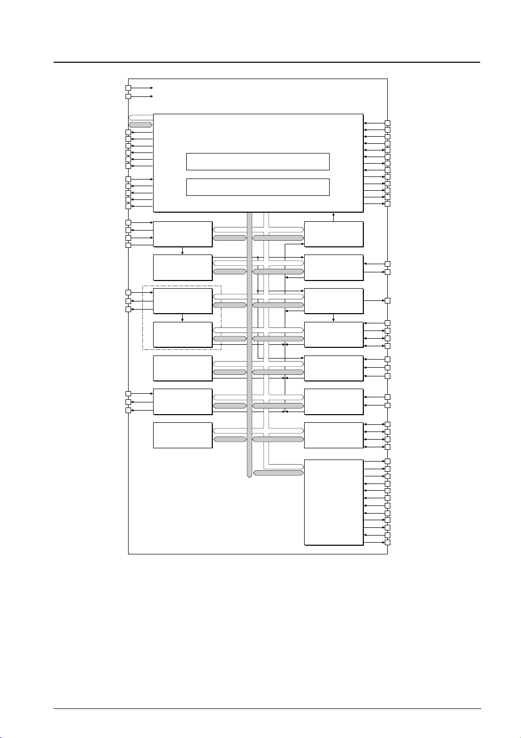
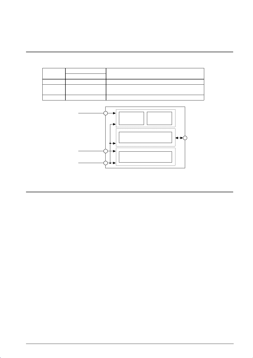
1.2 Block Diagram
VDD
VSS
1 OUTLINE
S1C33210
A[23:0]
D[15:0]
#WRL/#WR/#WE
#CE10EX #CE[9:4]
#DMAREQx(K50, K51)
#DMAACKx(P32, P33)
#DMAENDx(P15, P16)
#RD
#WRH/#BSH
#HCAS
#LCAS
#WAIT(P30)
#DRD(P20)
#DWE(P21)
#GAAS(P21)
#GARD(P31)
OSC3
OSC4
PLLS[1:0]
PLLC
OSC1
OSC2
FOSC1(P14)
OSC3/PLL
Prescaler
OSC1
Clock
Timer
Intelligent
DMA (128 ch.)
High-speed
DMA (4 ch.)
RAM
8KB
S1C33000
CPU Core
Bus Control Unit
Interrupt
Controller
16-bit
Programmable
Timer (6 ch.)
8-bit
Programmable
Timer (6 ch.)
Serial Interface
(4 ch.)
A/D Converter
(4 ch.)
Input Port
I/O Port
Mobile Access
Interface
#RESET
#NMI
#X2SPD
TST
DSIO
EA10MD[1:0]
BCLK
#BUSREQ(P34)
#BUSACK(P35)
#BUSGET(P31)
DST[2:0](P10–12)
DPCO(P13)
DCLK(P14)
EXCLx(P10–13, P15, P16)
TMx(P22–27)
T8UFx(P10–13)
SINx(P00, P04, P27, RXD)
SOUTx(P01, P05, P26, TXD)
#SCLKx(P02, P25)
#SRDYx(P03, P24)
AD0–3(K60–63)
#ADTRG(K52)
DD
AV
K50–52
K60–63
P00–05
P10–16
P20–27
P30–35
DTR
RTS
TXD
RI
CTS
DCD
DSR
RXD
CNT1
CNT2
MSEL
GOUT
Figure 1.2.1 S1C33210 Block Diagram
S1C33210 PRODUCT PART EPSON A-3
Page 18
1 OUTLINE
1.3 Pin Description
1.3.1 Pin Layout Diagram (plastic package)
QFP15-128pin
6596
No.
1
2
3
4
5
6
7
8
9
10
11
12
13
14
15
16
17
18
19
20
21
22
23
24
25
26
27
28
29
30
31
32
Pin name
P26/TM4/SOUT2
P27/TM5/SIN2
SS
V
BCLK
P00/SIN0
P01/SOUT0
D15
DD
V
P03/#SRDY0
D14
P31/#BUSGET/#GARD
D13
P32/#DMAACK0
D12
P33/#DMAACK1
D11
P02/#SCLK0
D10
K50/#DMAREQ0
#WRL/#WR/#WE
#WRH/#BSH
VSS
K51/#DMAREQ1
#RD
D9
D8
DD
V
K63/AD3
K62/AD2
AVDD
K61/AD1
K60/AD0
97
INDEX
128
No.
33
K52/#ADTRG
34
#CE10EX/#CE9&10EX
35
#CE4/#CE11/#CE11&12
36
D7
37
D6
38
D5
39
V
D4
40
D3
41
D2
42
#RESET
43
#NMI
44
D1
45
D0
46
V
47
#CE9/#CE17/#CE17&18
48
#CE7/#RAS0/#CE13/#RAS2
49
OSC2
50
OSC1
51
#CE6/#CE7&8
52
#CE8/#RAS1/#CE14/#RAS3
53
V
54
A0/#BSL
55
A1
56
A2
57
A3
58
P35/#BUSACK
59
#HCAS
60
#LCAS
61
P34/#BUSREQ/#CE6
62
A4
63
A5
64
Pin name
SS
DD
SS
No.
65
66
67
68
69
70
71
72
73
74
75
76
77
78
79
80
81
82
83
84
85
86
87
88
89
90
91
92
93
94
95
96
Pin name
A6
A7
SS
V
P30/#WAIT/#CE4&5
A8
A9
#CE5/#CE15/#CE15&16
A10
A20
DD
V
A11
A21
P16/EXCL5/#DMAEND1
A12
A22
TST
A13
A23
P04/SIN1
A14
A15
P05/SOUT1
A16
A17
A18
SS
V
A19
P20/#DRD
DD
V
RTS
DTR
DSR
Figure 1.3.1 Pin Layout Diagram (QFP15-128pin)
64
33
321
No.
97
98
99
100
101
102
103
104
105
106
107
108
109
110
111
112
113
114
115
116
117
118
119
120
121
122
123
124
125
126
127
128
Pin name
RI
CNT2
CNT1
TXD/SOUT3
CTS
SS
V
PLLC
V
SS
PLLS1
PLLS0
RXD/SIN3
DCD
MSEL
GOUT
DD
V
OSC3
OSC4
EA10MD0
EA10MD1
#X2SPD
P21/#DWE/#GAAS
P22/TM0
P23/TM1
DSIO
P10/EXCL0/T8UF0/DST0
P11/EXCL1/T8UF1/DST1
P12/EXCL2/T8UF2/DST2
P13/EXCL3/T8UF3/DPC0
P14/FOSC1/DCLK
P24/TM2/#SRDY2
P25/TM3/#SCLK2
P15/EXCL4/#DMAEND0
A-4 EPSON S1C33210 PRODUCT PART
Page 19
1.3.2 Pin Functions
Table 1.3.1 List of Pins for Power Supply System
Pin name Pin No. I/O Pull-up Function
QFP15-128
VDD 8, 27, 47, 74, 93, 111 ––Power supply (+)
VSS 3, 22, 39, 54, 67, 90,
102, 104
AVDD 30 ––Analog system power supply (+); AVDD = VDD
Table 1.3.2 List of Pins for External Bus Interface Signals
Pin name Pin No. I/O Pull-up Function
QFP15-128
A0
#BSL
A[23:1] 56-58, 63-66, 69, 70, 72,
75, 78, 81, 84, 85, 87-89,
D[15:0] 7, 10, 12, 14, 16, 18, 25, 26,
#CE10EX
#CE9&10EX
#CE9
#CE17
#CE17&18
#CE8
#RAS1
#CE14
#RAS3
#CE7
#RAS0
#CE13
#RAS2
#CE6
#CE7&8
#CE5
#CE15
#CE15&16
55 O – A0: Address bus (A0) when SBUSST(D3/0x4812E) = "0" (default)
91, 73, 76, 79, 82
36-38, 40-42, 45, 46
34 O – Area 10 chip enable for external memory
48 O – #CE9: Area 9 chip enable when CEFUNC[1:0](D[A:9])/0x48130) = "00"
53 O – #CE8: Area 8 chip enable when CEFUNC[1:0](D[A:9])/0x48130) = "00"
49 O – #CE7: Area 7 chip enable when CEFUNC[1:0](D[A:9])/0x48130) = "00"
52 O – Area 6 chip enable
71 O – #CE5: Area 5 chip enable when CEFUNC[1:0](D[A:9])/0x48130) = "00"
– (104
O – Address bus (A1 to A23)
I/O – Data bus (D0 to D15)
Power supply (-); GND
Pull-
down)
#BSL: Bus strobe (low byte) signal when SBUSST(D3/0x4812E) = "1"
* When CEFUNC[1:0] = "1x", this pin outputs #CE9+#CE10EX signal.
(default)
#CE17: Area 17 chip enable when CEFUNC[1:0](D[A:9])/0x48130) = "01"
* When CEFUNC[1:0] = "1x", this pin outputs #CE17+#CE18 signal.
and A8DRA(D8/0x48128) = "0" (default)
#RAS1: Area 8 DRAM row strobe when CEFUNC[1:0](D[A:9])/0x48130) =
"00" and A8DRA(D8/0x48128) = "1"
#CE14: Area 14 chip enable when CEFUNC[1:0](D[A:9])/0x48130) = "01"
or "1x" and A14DRA(D8/0x48122) = "0"
#RAS3: Area 14 DRAM row strobe when CEFUNC[1:0](D[A:9])/0x48130)
= "01"or "1x" and A14DRA(D8/0x48122) = "1"
and A7DRA(D7/0x48128) = "0" (default)
#RAS0: Area 7 DRAM row strobe when CEFUNC[1:0](D[A:9])/0x48130) =
"00" and A7DRA(D7/0x48128) = "1"
#CE13: Area 13 chip enable when CEFUNC[1:0](D[A:9])/0x48130) = "01"
or "1x" and A13DRA(D7/0x48122) = "0"
#RAS2: Area 13 DRAM row strobe when CEFUNC[1:0](D[A:9])/0x48130)
= "01" or "1x" and A13DRA(D7/0x48122) = "1"
* When CEFUNC[1:0] = "1x", this pin outputs #CE7+#CE8 signal.
(default)
#CE15: Area 15 chip enable when CEFUNC[1:0](D[A:9])/0x48130) = "01"
* When CEFUNC[1:0] = "1x", this pin outputs #CE15+#CE16 signal.
1 OUTLINE
S1C33210 PRODUCT PART EPSON A-5
Page 20
1 OUTLINE
Pin name Pin No. I/O Pull-up Function
QFP15-128
#CE4
#CE11
#CE11&12
#RD 24 O – Read signal
#WRL
#WR
#WE
#WRH
#BSH
#HCAS 60 O – #HCAS: DRAM column address strobe (high byte) signal
#LCAS 61 O – #LCAS: DRAM column address strobe (low byte) signal
BCLK 4 O – Bus clock output
P34
#BUSREQ
#CE6
P35
#BUSACK
P30
#WAIT
#CE4&5
P20
#DRD
P21
#DWE
#GAAS
P31
#BUSGET
#GARD
EA10MD1 115 I Pull-up Area 10 boot mode selection
EA10MD0 114 I – 10–
35 O – #CE4: Area 4 chip enable when CEFUNC[1:0](D[A:9])/0x48130) = "00"
(default)
#CE11: Area 11 chip enable when CEFUNC[1:0](D[A:9])/0x48130) = "01"
* When CEFUNC[1:0] = "1x", this pin outputs #CE11+#CE12 signal.
20 O – #WRL: Write (low byte) signal when SBUSST(D3/0x4812E) = "0" (default)
#WR: Write signal when SBUSST(D3/0x4812E) = "1"
#WE: DRAM write signal
21 O – #WRH: Write (high byte) signal when SBUSST(D3/0x4812E) = "0"
(default)
#BSH: Bus strobe (high byte) signal when SBUSST(D3/0x4812E) = "1"
62 I/O – P34: I/O port when CFP34(D4/0x402DC) = "0" (default)
#BUSREQ: Bus release request input when CFP34(D4/0x402DC) = "1"
#CE6: Area 6 chip enable when CFP34(D4/0x402DC) = "1" and
IOC34(D4/0x402DE) = "1"
59 I/O – P35: I/O port when CFP35(D5/0x402DC) = "0" (default)
#BUSACK: Bus acknowledge output when CFP35(D5/0x402DC) = "1"
68 I/O – P30: I/O port when CFP30(D0/0x402DC) = "0" (default)
#WAIT: Wait cycle request input when CFP30(D0/0x402DC) = "1"
#CE4&5: Areas 4&5 chip enable when CFP30(D0/0x402DC) = "1" and
IOC30(D0/0x402DE) = "1"
92 I/O – P20: I/O port when CFP20(D0/0x402D8) = "0" (default)
#DRD: DRAM read signal output for successive RAS mode when
CFP20(D0/0x402D8) = "1"
117 I/O – P21: I/O port when CFP21(D1/0x402D8) = "0" and
CFEX2(D2/0x402DF) = "0" (default)
#DWE: DRAM read signal output for successive RAS mode when
CFP21(D1/0x402D8) = "1" and CFEX2(D2/0x402DF) = "0"
#GAAS: Area address strobe for GA when CFEX2(D2/0x402DF) = "1"
11 I/O – P31: I/O port when CFP31(D1/0x402DC) = "0" and
CFEX3(D3/0x402DF) = "0" (default)
#BUSGET: Bus status monitor signal output when CFP31(D1/0x402DC) = "1"
and CFEX3(D3/0x402DF) = "0"
#GARD: Area read signal output for GA when CFEX3(D3/0x402DF) = "1"
EA10MD1 EA10MD0 Mode
1 1 External ROM mode
01–
00–
A-6 EPSON S1C33210 PRODUCT PART
Page 21
Table 1.3.3 List of Pins for HSDMA Control Signals
Pin name Pin No. I/O Pull-up Function
QFP15-128
K50
#DMAREQ0
K51
#DMAREQ1
P32
#DMAACK0
P33
#DMAACK1
P04
SIN1
P15
EXCL4
#DMAEND0
P16
EXCL5
#DMAEND1
P05
SOUT1
19 I Pull-up K50: Input port when CFK50(D0/0x402C0) = "0" (default)
#DMAREQ0: HSDMA Ch. 0 request input when CFK50(D0/0x402C0) = "1"
23 I Pull-up K51: Input port when CFK51(D1/0x402C0) = "0" (default)
#DMAREQ1: HSDMA Ch. 1 request input when CFK51(D1/0x402C0) = "1"
13 I/O – P32: I/O port when CFP32(D2/0x402DC) = "0" (default)
#DMAACK0: HSDMA Ch. 0 acknowledge output when CFP32(D2/0x402DC)
= "1"
15 I/O – P33: I/O port when CFP33(D3/0x402DC) = "0" (default)
#DMAACK1: HSDMA Ch. 1 acknowledge output when CFP33(D3/0x402DC)
= "1"
83 I/O – P04: I/O port when CFP04(D4/0x402D0) = "0" and
CFEX4(D4/0x402DF) = "0" (default)
SIN1: S erial I/F Ch. 1 data input when CFP04(D4/0x402D0) = "1" and
CFEX4(D4/0x402DF) = "0"
128 I/O – P15: I/O port when CFP15(D5/0x402D4) = "0" (default)
EXCL4: 16-bit timer 4 event counter input when CFP15(D5/0x402D4) =
"1" and IOC15(D5/0x402D6) = "0"
#DMAEND0: HSDMA Ch. 0 end-of-transfer signal output when
CFP15(D5/0x402D4) = "1" and IOC15(D5/0x402D6) = "1"
77 I/O – P16: I/O port when CFP16(D6/0x402D4) = "0" (default)
EXCL5: 16-bit timer 5 event counter input when CFP16(D6/0x402D4) =
"1" and IOC16(D6/0x402D6) = "0"
#DMAEND1: HSDMA Ch. 1 end-of-transfer signal output when
CFP16(D6/0x402D4) = "1" and IOC16(D6/0x402D6) = "1"
86 I/O – P05: I/O port when CFP05(D5/0x402D0) = "0" and
CFEX5(D5/0x402DF) = "0" (default)
SOUT1: Serial I/F Ch. 1 data output when CFP05(D5/0x402D0) = "1" and
CFEX5(D5/0x402DF) = "0"
1 OUTLINE
S1C33210 PRODUCT PART EPSON A-7
Page 22

1 OUTLINE
Table 1.3.4 List of Pins for Internal Peripheral Circuits
Pin name Pin No. I/O Pull-up Function
QFP15-128
K52
#ADTRG
K60
AD0
K61
AD1
K62
AD2
K63
AD3
P00
SIN0
P01
SOUT0
P02
#SCLK0
P03
#SRDY0
P04
SIN1
P05
SOUT1
P10
EXCL0
T8UF0
DST0
P11
EXCL1
T8UF1
DST1
P12
EXCL2
T8UF2
DST2
33 I Pull-up K52: Input port when CFK52(D2/0x402C0) = "0" (default)
#ADTRG: A/D converter trigger input when CFK52(D2/0x402C0) = "1"
32 I – K60: Input port when CFK60(D0/0x402C3) = "0" (default)
AD0: A/D converter Ch. 0 input when CFK60(D0/0x402C3) = "1"
31 I – K61: Input port when CFK61(D1/0x402C3) = "0" (default)
AD1: A/D converter Ch. 1 input when CFK61(D1/0x402C3) = "1"
29 I – K62: Input port when CFK62(D2/0x402C3) = "0" (default)
AD2: A/D converter Ch. 2 input when CFK62(D2/0x402C3) = "1"
28 I – K63: Input port when CFK63(D3/0x402C3) = "0" (default)
AD3: A/D converter Ch. 3 input when CFK63(D3/0x402C3) = "1"
5 I/O – P00: I/O port when CFP00(D0/0x402D0) = "0" (default)
SIN0: Serial I/F Ch. 0 data input when CFP00(D0/0x402D0) = "1"
6 I/O – P01: I/O port when CFP01(D1/0x402D0) = "0" (default)
SOUT0: Serial I/F Ch. 0 data output when CFP01(D1/0x402D0) = "1"
17 I/O – P02: I/O port when CFP02(D2/0x402D0) = "0" (default)
#SCLK0: Serial I/F Ch. 0 clock input/output when CFP02(D2/0x402D0) =
"1"
9 I/O – P03: I/O port when CFP03(D3/0x402D0) = "0" (default)
#SRDY0: Serial I/F Ch. 0 ready signal input/output when
CFP03(D3/0x402D0) = "1"
83 I/O – P04: I/O port when CFP04(D4/0x402D0) = "0" and
CFEX4(D4/0x402DF) = "0" (default)
SIN1: S erial I/F Ch. 1 data input when CFP04(D4/0x402D0) = "1" and
CFEX4(D4/0x402DF) = "0"
86 I/O – P05: I/O port when CFP05(D5/0x402D0) = "0" and
CFEX5(D5/0x402DF) = "0"(default)
SOUT1: Serial I/F Ch. 1 data output when CFP05(D5/0x402D0) = "1" and
CFEX5(D5/0x402DF) = "0"
121 I/O – P10: I/O port when CFP10(D0/0x402D4) = "0" and
CFEX1(D1/0x402DF) = "0"
EXCL0: 16-bit timer 0 event counter input when CFP10(D0/0x402D4) =
"1", IOC10(D0/0x402D6) = "0" and CFEX1(D1/0x402DF) = "0"
T8UF0: 8-bit timer 0 output when CFP10(D0/0x402D4) = "1",
IOC10(D0/0x402D6) = "1" and CFEX1(D1/0x402DF) = "0"
DST0: DST0 signal output when CFEX1(D1/0x402DF) = "1" (default)
122 I/O – P11: I/O port when CFP11(D1/0x402D4) = "0" and
CFEX1(D1/0x402DF) = "0"
EXCL1: 16-bit timer 1 event counter input when CFP11(D1/0x402D4) =
"1", IOC11(D1/0x402D6) = "0" and CFEX1(D1/0x402DF) = "0"
T8UF1: 8-bit timer 1 output when CFP11(D1/0x402D4) = "1",
IOC11(D1/0x402D6) = "1" and CFEX1(D1/0x402DF) = "0"
DST1: DST1 signal output when CFEX1(D1/0x402DF) = "1" (default)
123 I/O – P12: I/O port when CFP12(D2/0x402D4) = "0" and
CFEX0(D0/0x402DF) = "0"
EXCL2: 16-bit timer 2 event counter input when CFP12(D2/0x402D4) =
"1", IOC12(D2/0x402D6) = "0" and CFEX0(D0/0x402DF) = "0"
T8UF2: 8-bit timer 2 output when CFP12(D2/0x402D4) = "1",
IOC12(D2/0x402D6) = "1" and CFEX0(D0/0x402DF) = "0"
DST2: DST2 signal output when CFEX0(D0/0x402DF) = "1" (default)
A-8 EPSON S1C33210 PRODUCT PART
Page 23

Pin name Pin No. I/O Pull-up Function
QFP15-128
P13
EXCL3
T8UF3
DPCO
P14
FOSC1
DCLK
P15
EXCL4
#DMAEND0
P16
EXCL5
#DMAEND1
P20
#DRD
P21
#DWE
#GAAS
P22
TM0
P23
TM1
P24
TM2
#SRDY2
P25
TM3
#SCLK2
P26
TM4
SOUT2
P27
TM5
SIN2
124 I/O – P13: I/O port when CFP13(D3/0x402D4) = "0" and
CFEX1(D1/0x402DF) = "0"
EXCL3: 16-bit timer 3 event counter input when CFP13(D3/0x402D4) =
"1", IOC13(D3/0x402D6) = "0" and CFEX1(D1/0x402DF) = "0"
T8UF3: 8-bit timer 3 output when CFP13(D3/0x402D4) = "1",
IOC13(D3/0x402D6) = "1" and CFEX1(D1/0x402DF) = "0"
DPCO: DPCO signal output when CFEX1(D1/0x402DF) = "1" (default)
125 I/O – P14: I/O port when CFP14(D4/0x402D4) = "0" and
CFEX0(D0/0x402DF) = "0"
FOSC1: OSC1 clock output when CFP14(D4/0x402D4) = "1" and
CFEX0(D0/0x402DF) = "0"
DCLK: DCLK signal output when CFEX0(D0/0x402DF) = "1" (default)
128 I/O – P15: I/O port when CFP15(D5/0x402D4) = "0" (default)
EXCL4: 16-bit timer 4 event counter input when CFP15(D5/0x402D4) =
"1" and IOC15(D5/0x402D6) = "0"
#DMAEND0: HSDMA Ch. 0 end-of-transfer signal output when
CFP15(D5/0x402D4) = "1" and IOC15(D5/0x402D6) = "1"
77 I/O – P16: I/O port when CFP16(D6/0x402D4) = "0" (default)
EXCL5: 16-bit timer 5 event counter input when CFP16(D6/0x402D4) =
"1" and IOC16(D6/0x402D6) = "0"
#DMAEND1: HSDMA Ch. 1 end-of-transfer signal output when
CFP16(D6/0x402D4) = "1" and IOC16(D6/0x402D6) = "1"
92 I/O – P20: I/O port when CFP20(D0/0x402D8) = "0" (default)
#DRD: DRAM read signal output for successive RAS mode when
CFP20(D0/0x402D8) = "1"
117 I/O – P21: I/O port when CFP21(D1/0x402D8) = "0" and
CFEX2(D2/0x402DF) = "0" (default)
#DWE: DRAM read signal output for successive RAS mode when
CFP21(D1/0x402D8) = "1" and CFEX2(D2/0x402DF) = "0"
#GAAS: Area address strobe for GA when CFEX2(D2/0x402DF) = "1"
118 I/O – P22: I/O port when CFP22(D2/0x402D8) = "0" (default)
TM0: 16-bit timer 0 output when CFP22(D2/0x402D8) = "1"
119 I/O – P23: I/O port when CFP23(D3/0x402D8) = "0" (default)
TM1: 16-bit timer 1 output when CFP23(D3/0x402D8) = "1"
126 I/O – P24: I/O port when CFP24(D4/0x402D8) = "0" (default)
TM2: 16-bit timer 2 output when CFP24(D4/0x402D8) = "1"
#SRDY2: Serial I/F Ch.2 ready signal input/output when
SSRDY2(D3/0x402DB) = "1" and CFP24 (D4/0x402D8) = "0"
127 I/O – P25: I/O port when CFP25(D5/0x402D8) = "0" (default)
TM3: 16-bit timer 3 output when CFP25(D5/0x402D8) = "1"
#SCLK2: Serial I/F Ch.2 clock input/output when SSCLK2(D2/0x402DB) =
"1" and CFP25(D5/0x402D8) = "0"
1I/O– P26: I/O port when CFP26(D6/0x402D8) = "0" (default)
TM4: 16-bit timer 4 output when CFP26(D6/0x402D8) = "1"
SOUT2: Serial I/F Ch.2 data output when SSOUT2(D1/0x402DB) = "1"
and CFP26(D6/0x402D8) = "0"
2I/O– P27: I/O port when CFP27(D7/0x402D8) = "0" (default)
TM5: 16-bit timer 5 output when CFP27(D7/0x402D8) = "1"
SIN2: S erial I/F Ch.2 data input when SSIN2(D0/0x402DB) = "1" and
CFP27(D7/0x402D8) = "0"
1 OUTLINE
S1C33210 PRODUCT PART EPSON A-9
Page 24
1 OUTLINE
Pin name Pin No. I/O Pull-up Function
QFP15-128
DTR 95 O – DTR output *1
RTS 94 O – RTS output*1
TXD
SOUT3
RI 97 I – RI input *1
CTS 101 I – CTS input *1
DCD 108 I – DCD input *1
DSR 96 I – DSR input *1
RXD
SIN3
CNT1 99 O – Mobile access control output #1
CNT2 98 O – Mobile access control output #2
MSEL 109 I Pull-up Serial I/O interface Ch. 3 configuration input. Normally drive this at High level.
GOUT 110 O – NMI interrupt request output
100 O – TXD: TXD output*1 when MSEL pin input is at High level
SOUT3: SOUT3 output when MSEL pin input is at Low level
107 I – RXD: RXD input when MSEL pin input is at High level
SIN3: SIN3 input when MSEL pin input is at Low level
Note: *1 The communications macro select (MCRS) register (D[1:0]/0x200000) configures the I/O
signals to match the target mobile device.
Table 1.3.5 List of Pins for Clock Generator
Pin name Pin No. I/O Pull-up Function
QFP15-128
OSC1 51 I – Low-speed (OSC1) oscillation input (32 kHz crystal oscillator or external clock
input)
OSC2 50 O – Low-speed (OSC1) oscillation output
OSC3 112 I – High-speed (OSC3) oscillation input (crystal/ceramic oscillator or external clock
input)
OSC4 113 O – High-speed (OSC3) oscillation output
PLLS[1:0] 105,106 I – PLL set-up pins
PLLS1 PLLS0 fin (f OSC3) fout (fPSCIN)
1110–25MHz 20–50MHz
0110–12.5MHz 40–50MHz
0 0 PLL is not
used
L
PLLC 103 ––Capasitor connecting pin for PLL
Table 1.3.6 List of Other Pins
Pin name Pin No. I/O Pull-up Function
QFP15-128 /down
TST 80 I Pull-
DSIO 120 I/O Pull-up Serial I/O pin for debugging
#X2SPD 116 I – Clock doubling mode set-up pin1: CPU clock = bus clock × 1, 0: CPU clock = bus
#NMI 44 I Pull-up NMI request input pin
#RESET 43 I Pull-up Initial reset input pin
Test mode input. This pin is used for testing this chip. For further details, refer
down
to the S1C33 ASIC Design Guide.
This pin is used to communicate with the debugging tool S5U1C33000H.
clock × 2
Note:"#" in the pin names indicates that the signal is low active.
A-10 EPSON S1C33210 PRODUCT PART
Page 25
2 Power Supply
This chapter explains the operating voltage of the S1C33210.
2.1 Power Supply Pins
The S1C33210 has the power supply pins shown in Table 2.1.1.
Table 2.1.1 Power Supply Pins
Pin name Pin No. Function
QFP15-128
VDD 8, 27, 47, 74, 93, 111 Power supply (+)
VSS 3, 22, 39, 54, 67, 90,
102, 104
AVDD 30 Analog system power supply (+); AVDD = VDD
Power supply (-); GND
2 POWER SUPPLY
2.7 to 3.6 V
2.7 to 3.6 V
GND
VDD
CPU core
I/O
interface circuit
AVDD
Analog circuits
(A/D converter)
VSS
Figure 2.1.1 Power Supply System
Internal
peripheral
circuit
I/O pins
2.2 Operating Voltage (VDD, VSS)
The core CPU, internal peripheral circuits, and external signal interfaces operate on the voltage difference between
the V
DD and VSS pins. The following operating voltage can be used:
DD = 2.7 V to 3.6 V (VSS = GND)
V
Note: The S1C33210 has 6 V
pins. Do not open any of them.
The operating clock frequency range (OSC3) is 5 MHz to 50 MHz with this voltage.
DD pins and 8 VSS pins. Be sure to supply the operating voltage to all the
S1C33210 PRODUCT PART EPSON A-11
Page 26

2 POWER SUPPLY
2.3 Power Supply for Analog Circuits (AVDD)
The analog power supply pin (AVDD) is provided separately from the V DD and VDD pins in order that the digital
circuits do not affect the analog circuit (A/D converter). The AV
the V
SS pin is used as the analog ground.
Supply the same voltage level as the V
DD = V DD, V SS = GND
AV
Note: Be sure to supply V
DD to the AVDD pin even if the analog circuit is not used.
DD to the AVDD pin.
Noise on the analog power lines decrease the A/D converting precision, so use a stabilized power supply and make
the board pattern with consideration given to that.
DD pin is used to supply an analog power voltage and
A-12 EPSON S1C33210 PRODUCT PART
Page 27
3 INTERNAL MEMORY
3 Internal Memory
This chapter explains the internal memory configuration.
Figure 3.1 shows the S1C33210 memory map.
Area Address
Areas 18–11
Area 10
Areas 9
Area 6
Area 5
Area 4 0x01FFFFF
Area 3
Area 2
Area 1
Area 0
–7
0xFFFFFFF
0x1000000
0x0FFFFFF
0x0C00000
0x0BFFFFF
0x0400000
0x03FFFFF
0x0380000
0x037FFFF
0x0300000
0x02FFFFF
0x0200000
0x0100000
0x00FFFFF
0x0080000
0x007FFFF
0x0060000
0x005FFFF
0x0050000
0x004FFFF
0x0040000
0x003FFFF
0x0030000
0x002FFFF
0x0002000
0x0001FFF
0x0000000
Figure 3.1 Memory Map
Area 2 is used in debug mode only and it cannot be accessed in user mode (normal program execution status).
S1C33210
External Memory
External Memory
External Memory
External I/O (16-bit device)
External I/O (8-bit device)
Internal peripheral circuits
External Memory
(Reserved)
For middleware use
(Reserved)
For CPU, debug mode
(Mirror of internal
peripheral circuits)
Internal peripheral circuits
(Mirror of internal
peripheral circuits)
(Mirror of internal RAM)
Internal RAM (8KB)
3.1 ROM and Boot Address
The S1C33210 does not have a built-in ROM. The boot address is fixed at 0x0C00000, and so external ROM/Flash
should be used in Area 10.
For setting up Area 10, refer to the "BCU (Bus Controller Unit)" in "S1C33210 FUNCTION PART" in this manual.
3.2 RAM
The S1C33210 has a built-in 8KB RAM. The RAM is allocated to Area 0, address 0x0000000 to address
0x0001FFF.
The internal RAM is a 32-bit sized device and data can be read/written in 1 cycle regardless of data size (byte, halfword or word).
S1C33210 PRODUCT PART EPSON A-13
Page 28

4 PERIPHERAL CIRCUITS
4 Peripheral Circuits
This chapter lists the built-in peripheral circuits and the I/O memory map. For details of the circuits, refer to the
"S1C33210 FUNCTION PART".
4.1 List of Peripheral Circuits
The S1C33210 consists of the C33 Core Block, C33 Peripheral Block, C33 DMA Block and C33 Analog Block.
C33 Core Block
CPU S1C33000 32-bit RISC type CPU
BCU (Bus Control Unit) 24-bit external address bus and 16-bit data bus
All the BCU functions can be used.
ITC (Interrupt Controller) 39 types of interrupts are available.
CLG (Clock Generator) OSC3 oscillation circuit (33 MHz Max.), PLL and OSC1 oscillation circuit
(32.768 kHz Typ.) built-in
DBG (Debug Unit) Functional block for debugging with the S5U1C33000H (In-Circuit Debugger
for S1C33 Family)
C33 Peripheral Block
Prescaler Programmable clock generator for peripheral circuits
8-bit programmable timer 6 channels with clock output function
16-bit programmable timer 6 channels with event counter, clock output and watchdog timer functions
Serial interface 4 channels (asynchronous mode, clock synchronous mode and IrDA are
selectable. Interfaces 1 and 3 support only asynchronous operation.)
Input and I/O ports 7 bits of input ports and 27 bits of I/O ports (used for peripheral I/O)
Clock timer 1 channel with alarm function
Mobile access interfaces One PHS, PDC, and HDLC interface each
C33 DMA Block
HSDMA (High-Speed DMA) 4 channels (Only two interfaces support external requests.)
IDMA (Intelligent DMA) 128 channels
C33 Analog Block
A/D converter 10-bit A/D converter with 4 input channels
A-14 EPSON S1C33210 PRODUCT PART
Page 29
4.2 I/O Memory Map
NameAddressRegister name Bit Function Setting Init. R/W Remarks
–
8-bit timer 4/5
clock select
register
8-bit timer 4/5
clock control
register
8-bit timer
clock select
register
16-bit timer 0
clock control
register
16-bit timer 1
clock control
register
16-bit timer 2
clock control
register
0040140
0040145
0040146
0040147
0040148
0040149
(B)
(B)
(B)
(B)
(B)
(B)
D7–2
D1
D0
D7
D6
D5
D4
D3
D2
D1
D0
D7–4
D3
D2
D1
D0
D7–4
D3
D2
D1
D0
D7–4
D3
D2
D1
D0
D7–4
D3
D2
D1
D0
P8TPCK5
P8TPCK4
P8TS52
P8TS51
P8TS50
P8TON4
P8TS42
P8TS41
P8TS40
P8TPCK3
P8TPCK2
P8TPCK1
P8TPCK0
P16TON0
P16TS02
P16TS01
P16TS00
P16TON1
P16TS12
P16TS11
P16TS10
P16TON2
P16TS22
P16TS21
P16TS20
Table 4.2.1 I/O Memory Map
reserved
8-bit timer 5 clock selection
8-bit timer 4 clock selection
8-bit timer 5 clock control
8-bit timer 5
clock division ratio selection
8-bit timer 4 clock control
8-bit timer 4
clock division ratio selection
reserved
8-bit timer 3 clock selection
8-bit timer 2 clock selection
8-bit timer 1 clock selection
8-bit timer 0 clock selection
reserved
16-bit timer 0 clock control
16-bit timer 0
clock division ratio selection
reserved
16-bit timer 1 clock control
16-bit timer 1
clock division ratio selection
reserved
16-bit timer 2 clock control
16-bit timer 2
clock division ratio selection
1 θ/1 0 Divided clk.
1 θ/1 0 Divided clk.
1 On 0 OffP8TON5
1
1
1
1
0
0
0
0
1 On 0 Off
1
1
1
1
0
0
0
0
1 θ/1 0 Divided clk.
1 θ/1 0 Divided clk.
1 θ/1 0 Divided clk.
1 θ/1 0 Divided clk.
1 On 0 Off
P16TS0[2:0] Division ratio
1
1
1
1
0
0
0
0
1 On 0 Off
P16TS1[2:0] Division ratio
1
1
1
1
0
0
0
0
1 On 0 Off
P16TS2[2:0] Division ratio
1
1
1
1
0
0
0
0
–
1
1
1
0
0
1
1
0
0
1
1
0
0
1
1
0
0
1
1
0
0
1
1
0
0
1
1
0
0
1
1
0
0
1
1
0
0
1
1
0
0
θ/256
0
θ/128
1
θ/64
0
θ/32
1
θ/16
0
θ/8
1
θ/4
0
θ/2
1
θ/4096
0
θ/2048
1
θ/64
0
θ/32
1
θ/16
0
θ/8
1
θ/4
0
θ/2
––
––
1
θ/4096
0
θ/1024
1
θ/256
0
θ/64
1
θ/16
0
θ/4
1
θ/2
0
θ/1
––
1
θ/4096
0
θ/1024
1
θ/256
0
θ/64
1
θ/16
0
θ/4
1
θ/2
0
θ/1
––
1
θ/4096
0
θ/1024
1
θ/256
0
θ/64
1
θ/16
0
θ/4
1
θ/2
0
θ/1
4 PERIPHERAL CIRCUITS
–
–
0 when being read.
0
R/W
θ: selected by
0
R/W
Prescaler clock select
register (0x40181)
0
R/W
θ: selected by
0
R/W
Prescaler clock select
0
R/W
register (0x40181)
0
R/W
8-bit timer 5 can
generate the clock for
the serial I/F Ch.3.
0
R/W
θ: selected by
0
R/W
Prescaler clock select
0
R/W
register (0x40181)
0
R/W
8-bit timer 4 can
generate the clock for
the serial I/F Ch.2.
–
–
0 when being read.
0
R/W
θ: selected by
0
R/W
Prescaler clock select
0
R/W
register (0x40181)
0
R/W
–
–
0 when being read.
0
R/W
θ: selected by
0
R/W
Prescaler clock select
0
register (0x40181)
0
16-bit timer 0 can be
used as a watchdog
timer.
–
–
0 when being read.
0
R/W
θ: selected by
0
R/W
Prescaler clock select
0
register (0x40181)
0
–
–
0 when being read.
0
R/W
θ: selected by
0
R/W
Prescaler clock select
0
register (0x40181)
0
(B) in [Address] indicates an 8-bit register and (HW) indicates a 16-bit register.
The meaning of the symbols described in [Init.] are listed below:
0, 1: Initial values that are set at initial reset.
(However, the registers for the bus and input/output ports are not initialized at hot start.)
X: Not initialized at initial reset.
–: Not set in the circuit.
S1C33210 PRODUCT PART EPSON A-15
Page 30
4 PERIPHERAL CIRCUITS
16-bit timer 3
clock control
register
16-bit timer 4
clock control
register
16-bit timer 5
clock control
register
8-bit timer 0/1
clock control
register
004014A
004014B
004014C
004014D
(B)
(B)
(B)
(B)
D7–4
D3
D2
D1
D0
D7–4
D3
D2
D1
D0
D7–4
D3
D2
D1
D0
D7
D6
D5
D4
D3
D2
D1
D0
NameAddressRegister name Bit Function Setting Init. R/W Remarks
P16TON3
P16TS32
P16TS31
P16TS30
P16TON4
P16TS42
P16TS41
P16TS40
P16TON5
P16TS52
P16TS51
P16TS50
P8TS12
P8TS11
P8TS10
P8TON0
P8TS02
P8TS01
P8TS00
reserved
16-bit timer 3 clock control
16-bit timer 3
clock division ratio selection
reserved
16-bit timer 4 clock control
16-bit timer 4
clock division ratio selection
reserved
16-bit timer 5 clock control
16-bit timer 5
clock division ratio selection
8-bit timer 1 clock control
8-bit timer 1
clock division ratio selection
8-bit timer 0 clock control
8-bit timer 0
clock division ratio selection
1 On 0 Off
P16TS3[2:0] Division ratio
1
1
1
1
0
0
0
0
1 On 0 Off
P16TS4[2:0] Division ratio
1
1
1
1
0
0
0
0
1 On 0 Off
P16TS5[2:0] Division ratio
1
1
1
1
0
0
0
0
1 On 0 OffP8TON1
P8TS1[2:0] Division ratio
1
1
1
1
0
0
0
0
1 On 0 Off
P8TS0[2:0] Division ratio
1
1
1
1
0
0
0
0
––
1
1
1
0
0
1
1
0
0
1
1
0
0
1
1
0
0
1
1
0
0
1
1
0
0
1
1
0
0
1
1
0
0
1
1
0
0
1
1
0
0
θ/4096
0
θ/1024
1
θ/256
0
θ/64
1
θ/16
0
θ/4
1
θ/2
0
θ/1
––
1
θ/4096
0
θ/1024
1
θ/256
0
θ/64
1
θ/16
0
θ/4
1
θ/2
0
θ/1
––
1
θ/4096
0
θ/1024
1
θ/256
0
θ/64
1
θ/16
0
θ/4
1
θ/2
0
θ/1
1
θ/4096
0
θ/2048
1
θ/1024
0
θ/512
1
θ/256
0
θ/128
1
θ/64
0
θ/32
1
θ/256
0
θ/128
1
θ/64
0
θ/32
1
θ/16
0
θ/8
1
θ/4
0
θ/2
–
–
0
R/W
0
R/W
0
0
–
–
0
R/W
0
R/W
0
0
–
–
0
R/W
0
R/W
0
0
0
R/W
0
R/W
0
0
R/W
0
R/W
0
0
0
0 when being read.
θ: selected by
Prescaler clock select
register (0x40181)
0 when being read.
θ: selected by
Prescaler clock select
register (0x40181)
0 when being read.
θ: selected by
Prescaler clock select
register (0x40181)
θ: selected by
Prescaler clock select
register (0x40181)
8-bit timer 1 can
generate the OSC3
oscillation-stabilize
waiting period.
θ: selected by
Prescaler clock select
register (0x40181)
8-bit timer 0 can
generate the DRAM
refresh clock.
A-16 EPSON S1C33210 PRODUCT PART
Page 31

8-bit timer 2/3
clock control
register
A/D clock
control register
Run/Stop
register
Clock timer
interrupt
control register
Clock timer
divider register
Clock timer
second
register
004014E
(B)
004014F
(B)
0040151
(B)
0040152
(B)
0040153
(B)
(B)
4 PERIPHERAL CIRCUITS
NameAddressRegister name Bit Function Setting Init. R/W Remarks
D7
D6
D5
D4
D3
D2
D1
D0
D7–4
D3
D2
D1
D0
D7–2
D1
D0
D7
D6
D5
D4
D3
D2
D1
D0
D7
D6
D5
D4
D3
D2
D1
D0
D7–6
D5
D4
D3
D2
D1
D0
P8TS32
P8TS31
P8TS30
P8TON2
P8TS22
P8TS21
P8TS20
–
PSONAD
PSAD2
PSAD1
PSAD0
–
TCRST
TCRUN
TCISE2
TCISE1
TCISE0
TCASE2
TCASE1
TCASE0
TCIF
TCAF
TCD7
TCD6
TCD5
TCD4
TCD3
TCD2
TCD1
TCD0
–
TCMD5
TCMD4
TCMD3
TCMD2
TCMD1
TCMD0
8-bit timer 3 clock control
8-bit timer 3
clock division ratio selection
8-bit timer 2 clock control
8-bit timer 2
clock division ratio selection
reserved
A/D converter clock control
A/D converter clock division ratio
selection
reserved
Clock timer reset
Clock timer Run/Stop control
Clock timer interrupt factor
selection
Clock timer alarm factor selection
Interrupt factor generation flag
Alarm factor generation flag
Clock timer data 1 Hz
Clock timer data 2 Hz
Clock timer data 4 Hz
Clock timer data 8 Hz
Clock timer data 16 Hz
Clock timer data 32 Hz
Clock timer data 64 Hz
Clock timer data 128 Hz
reserved
Clock timer second counter data
TCMD5 = MSB
TCMD0 = LSB
1 On 0 OffP8TON3
P8TS3[2:0] Division ratio
1
1
1
1
1
1
0
1
0
0
1
0
1
0
0
0
0
1 On 0 Off
P8TS2[2:0] Division ratio
1
1
1
1
1
0
1
0
0
1
0
1
0
0
0
0
θ/256
0
θ/128
1
θ/64
0
θ/32
1
θ/16
0
θ/8
1
θ/4
0
θ/2
1
θ/4096
0
θ/2048
1
θ/64
0
θ/32
1
θ/16
0
θ/8
1
θ/4
0
θ/2
–
1 On 0 Off
P8TS0[2:0] Division ratio
1
1
1
1
1
1
0
1
0
0
1
0
1
0
0
0
0
1 Reset 0 Invalid
1 Run 0 Stop
θ/256
0
θ/128
1
θ/64
0
θ/32
1
θ/16
0
θ/8
1
θ/4
0
θ/2
–Clock timer
TCISE[2:0] Interrupt factor
1
1
1
1
1
1
0
1
0
0
1
0
1
0
0
0
0
None
0
Day
1
Hour
0
Minute
1
1 Hz
0
2 Hz
1
8 Hz
0
32 Hz
TCASE[2:0] Alarm factor
1
X
X
X
1
0
Day
Hour
Minute
None
Not generated
Not generated
–
X
1
X
X
0
0
1 Generated 0
1 Generated 0
1 High 0 Low
1 High 0 Low
1 High 0 Low
1 High 0 Low
1 High 0 Low
1 High 0 Low
1 High 0 Low
1 High 0 Low
0 to 59 seconds
0
0
0
0
0
0
0
0
–
0
0
0
0
–
X
X
X
X
X
X
X
X
X
X
X
X
X
X
X
X
X
X
–
X
X
X
X
X
X
R/W
θ: selected by
R/W
Prescaler clock select
register (0x40181)
8-bit timer 3 can
generate the clock for
the serial I/F Ch.1.
R/W
R/W
θ: selected by
Prescaler clock select
register (0x40181)
8-bit timer 2 can
generate the clock for
the serial I/F Ch.0.
–
0 when being read.
R/W
θ: selected by
R/W
Prescaler clock select
register (0x40181)
–
0 when being read.
W
0 when being read.
R/W
R/W
R/W
R/W
Reset by writing 1.
R/W
Reset by writing 1.
R
R
R
R
R
R
R
R
–R0 when being read.0040154
S1C33210 PRODUCT PART EPSON A-17
Page 32

4 PERIPHERAL CIRCUITS
Clock timer
minute register
Clock timer
hour register
Clock timer
day (low-order)
register
Clock timer
day (highorder) register
minute
comparison
register
hour
comparison
register
day
comparison
register
0040158
004015B
(B)
(B)
(B)
(B)
(B)
(B)
(B)
D7–6
D5
D4
D3
D2
D1
D0
D7–5
D4
D3
D2
D1
D0
D7
D6
D5
D4
D3
D2
D1
D0
D7
D6
D5
D4
D3
D2
D1
D0
D7–6
D5
D4
D3
D2
D1
D0
D7–5
D4
D3
D2
D1
D0
D7–5
D4
D3
D2
D1
D0
NameAddressRegister name Bit Function Setting Init. R/W Remarks
–
TCHD5
TCHD4
TCHD3
TCHD2
TCHD1
TCHD0
–
TCDD4
TCDD3
TCDD2
TCDD1
TCDD0
TCND7
TCND6
TCND5
TCND4
TCND3
TCND2
TCND1
TCND0
TCND14
TCND13
TCND12
TCND11
TCND10
TCND9
TCND8
–
TCCH5
TCCH4
TCCH3
TCCH2
TCCH1
TCCH0
–
TCCD4
TCCD3
TCCD2
TCCD1
TCCD0
–
TCCN4
TCCN3
TCCN2
TCCN1
TCCN0
reserved
Clock timer minute counter data
TCHD5 = MSB
TCHD0 = LSB
reserved
Clock timer hour counter data
TCDD4 = MSB
TCDD0 = LSB
Clock timer day counter data
(low-order 8 bits)
TCND0 = LSB
Clock timer day counter data
(high-order 8 bits)
TCND15 = MSB
reserved
Clock timer minute comparison
data
TCCH5 = MSB
TCCH0 = LSB
reserved
Clock timer hour comparison data
TCCD4 = MSB
TCCD0 = LSB
reserved
Clock timer day comparison data
TCCN4 = MSB
TCCN0 = LSB
–
0 to 59 minutes
–
0 to 23 hours
0 to 65535 days
(low-order 8 bits)
0 to 65535 days
(high-order 8 bits)
–Clock timer
0 to 59 minutes
(Note) Can be set within 0–63.
–Clock timer
0 to 23 hours
(Note) Can be set within 0–31.
–Clock timer
0 to 31 days
–
X
R/W
X
X
X
X
X
–
X
R/W
X
X
X
X
X
R/W0040157
X
X
X
X
X
X
X
X
R/WTCND15
X
X
X
X
X
X
X
–
X
R/W
X
X
X
X
X
–
X
R/W
X
X
X
X
–
X
R/W
X
X
X
X
–
0 when being read.0040155
–
0 when being read.0040156
–
0 when being read.0040159
–
0 when being read.004015A
–
0 when being read.
Compared with
TCND[4:0].
A-18 EPSON S1C33210 PRODUCT PART
Page 33

8-bit timer 0
control register
8-bit timer 0
reload data
register
8-bit timer 0
counter data
register
8-bit timer 1
control register
8-bit timer 1
reload data
register
8-bit timer 1
counter data
register
8-bit timer 2
control register
8-bit timer 2
reload data
register
8-bit timer 2
counter data
register
0040160
(B)
(B)
(B)
0040164
(B)
(B)
(B)
0040168
(B)
(B)
(B)
4 PERIPHERAL CIRCUITS
NameAddressRegister name Bit Function Setting Init. R/W Remarks
–
D7–3
D2
D1
D0
D7
D6
D5
D4
D3
D2
D1
D0
D7
D6
D5
D4
D3
D2
D1
D0
D7–3
D2
D1
D0
D7
D6
D5
D4
D3
D2
D1
D0
D7
D6
D5
D4
D3
D2
D1
D0
D7–3
D2
D1
D0
D7
D6
D5
D4
D3
D2
D1
D0
D7
D6
D5
D4
D3
D2
D1
D0
PTOUT0
PSET0
PTRUN0
RLD06
RLD05
RLD04
RLD03
RLD02
RLD01
RLD00
PTD06
PTD05
PTD04
PTD03
PTD02
PTD01
PTD00
–
PTOUT1
PSET1
PTRUN1
RLD16
RLD15
RLD14
RLD13
RLD12
RLD11
RLD10
PTD16
PTD15
PTD14
PTD13
PTD12
PTD11
PTD10
–
PTOUT2
PSET2
PTRUN2
RLD26
RLD25
RLD24
RLD23
RLD22
RLD21
RLD20
PTD26
PTD25
PTD24
PTD23
PTD22
PTD21
PTD20
reserved
8-bit timer 0 clock output control
8-bit timer 0 preset
8-bit timer 0 Run/Stop control
8-bit timer 0 reload data
RLD07 = MSB
RLD00 = LSB
8-bit timer 0 counter data
PTD07 = MSB
PTD00 = LSB
reserved
8-bit timer 1 clock output control
8-bit timer 1 preset
8-bit timer 1 Run/Stop control
8-bit timer 1 reload data
RLD17 = MSB
RLD10 = LSB
8-bit timer 1 counter data
PTD17 = MSB
PTD10 = LSB
reserved
8-bit timer 2 clock output control
8-bit timer 2 preset
8-bit timer 2 Run/Stop control
8-bit timer 2 reload data
RLD27 = MSB
RLD20 = LSB
8-bit timer 2 counter data
PTD27 = MSB
PTD20 = LSB
1 On 0 Off
–
1 Preset 0 Invalid
1 Run 0 Stop
0 to 255RLD07
0 to 255PTD07
–
1 On 0 Off
1 Preset 0 Invalid
1 Run 0 Stop
0 to 255RLD17
0 to 255PTD17
–
1 On 0 Off
1 Preset 0 Invalid
1 Run 0 Stop
0 to 255RLD27
0 to 255PTD27
–
0
–
0
X
X
X
X
X
X
X
X
X
X
X
X
X
X
X
X
–
0
–
0
X
X
X
X
X
X
X
X
X
X
X
X
X
X
X
X
–
0
–
0
X
X
X
X
X
X
X
X
X
X
X
X
X
X
X
X
–
0 when being read.
R/W
W
0 when being read.
R/W
R/W0040161
R0040162
–
0 when being read.
R/W
0 when being read.
W
R/W
R/W0040165
R0040166
–
0 when being read.
R/W
0 when being read.
W
R/W
R/W0040169
R004016A
S1C33210 PRODUCT PART EPSON A-19
Page 34

4 PERIPHERAL CIRCUITS
8-bit timer 3
control register
8-bit timer 3
reload data
register
8-bit timer 3
counter data
register
8-bit timer 4
control register
8-bit timer 4
reload data
register
8-bit timer 4
counter data
register
8-bit timer 5
control register
8-bit timer 5
reload data
register
8-bit timer 5
counter data
register
004016C
0040174
0040178
(B)
(B)
(B)
(B)
(B)
(B)
(B)
(B)
(B)
D7–3
D2
D1
D0
D7
D6
D5
D4
D3
D2
D1
D0
D7
D6
D5
D4
D3
D2
D1
D0
D7–3
D2
D1
D0
D7
D6
D5
D4
D3
D2
D1
D0
D7
D6
D5
D4
D3
D2
D1
D0
D7–3
D2
D1
D0
D7
D6
D5
D4
D3
D2
D1
D0
D7
D6
D5
D4
D3
D2
D1
D0
NameAddressRegister name Bit Function Setting Init. R/W Remarks
–
PTOUT3
PSET3
PTRUN3
RLD36
RLD35
RLD34
RLD33
RLD32
RLD31
RLD30
PTD36
PTD35
PTD34
PTD33
PTD32
PTD31
PTD30
–
PTOUT4
PSET4
PTRUN4
RLD46
RLD45
RLD44
RLD43
RLD42
RLD41
RLD40
PTD46
PTD45
PTD44
PTD43
PTD42
PTD41
PTD40
–
PTOUT5
PSET5
PTRUN5
RLD56
RLD55
RLD54
RLD53
RLD52
RLD51
RLD50
PTD56
PTD55
PTD54
PTD53
PTD52
PTD51
PTD50
reserved
8-bit timer 3 clock output control
8-bit timer 3 preset
8-bit timer 3 Run/Stop control
8-bit timer 3 reload data
RLD37 = MSB
RLD30 = LSB
8-bit timer 3 counter data
PTD37 = MSB
PTD30 = LSB
reserved
8-bit timer 4 clock output control
8-bit timer 4 preset
8-bit timer 4 Run/Stop control
8-bit timer 4 reload data
RLD47 = MSB
RLD40 = LSB
8-bit timer 4 counter data
PTD47 = MSB
PTD40 = LSB
reserved
8-bit timer 5 clock output control
8-bit timer 5 preset
8-bit timer 5 Run/Stop control
8-bit timer 5 reload data
RLD57 = MSB
RLD50 = LSB
8-bit timer 5 counter data
PTD57 = MSB
PTD50 = LSB
1 On 0 Off
–
1 Preset 0 Invalid
1 Run 0 Stop
0 to 255RLD37
0 to 255PTD37
–
1 On 0 Off
1 Preset 0 Invalid
1 Run 0 Stop
0 to 255RLD47
0 to 255PTD47
–
1 On 0 Off
1 Preset 0 Invalid
1 Run 0 Stop
0 to 255RLD57
0 to 255PTD57
–
0
R/W
–
0
R/W
X
R/W004016D
X
X
X
X
X
X
X
X
X
X
X
X
X
X
X
–
0
R/W
–
0
R/W
X
R/W0040175
X
X
X
X
X
X
X
X
X
X
X
X
X
X
X
–
0
R/W
–
0
R/W
X
R/W0040179
X
X
X
X
X
X
X
X
X
X
X
X
X
X
X
–
0 when being read.
W
0 when being read.
R004016E
–
0 when being read.
0 when being read.
W
R0040176
–
0 when being read.
0 when being read.
W
R004017A
A-20 EPSON S1C33210 PRODUCT PART
Page 35

Watchdog
timer writeprotect register
Watchdog
timer enable
register
0040170
(B)
0040171
(B)
4 PERIPHERAL CIRCUITS
NameAddressRegister name Bit Function Setting Init. R/W Remarks
WRWD
D7
D6–0
D7–2
D1
D0
–
–
EWD
–
EWD write protection
–
–
Watchdog timer enable
–
1
Write enabled0Write-protect
1
NMI enabled0NMI disabled
–
–
–
0–R/W
–
0
–
0 when being read.
–
–
0 when being read.
R/W
0 when being read.
–
S1C33210 PRODUCT PART EPSON A-21
Page 36

4 PERIPHERAL CIRCUITS
Power control
register
select register
Clock option
register
Power control
protect register
0040180
0040181
0040190
(B)
(B)
(B)
(B)
D7
D6
D5
D4–3
D2
D1
D0
D7–1
D0
D7–4
D3
D2
D1
D0
D7
D6
D5
D4
D3
D2
D1
D0
NameAddressRegister name Bit Function Setting Init. R/W Remarks
CLKDT1
CLKDT0
PSCON
–
CLKCHG
SOSC3
SOSC1
–
PSCDT0
–
HLT2OP
8T1ON
–
PF1ON
CLGP7
CLGP6
CLGP5
CLGP4
CLGP3
CLGP2
CLGP1
CLGP0
System clock division ratio
selection
Prescaler On/Off control
reserved
CPU operating clock switch
High-speed (OSC3) oscillation On/Off
Low-speed (OSC1) oscillation On/Off
reserved
Prescaler clock selection
–
HALT clock option
OSC3-stabilize waiting function
reserved
OSC1 external output control
Power control register protect flag 0
CLKDT[1:0] Division ratio
1
1
1
0
0
1
0
0
1 On 0 Off
1 OSC3 0 OSC1
1 On 0 Off
1 On 0 Off
1 OSC1 0 OSC3/PLL
1/8
1/4
1/2
1/1
–
–Prescaler clock
–
1 On 0 Off
1 Off 0 On
–
1 On 0 Off
Writing 10010110 (0x96)
removes the write protection of
the power control register
(0x40180) and the clock option
register (0x40190).
Writing another value set the
write protection.
0
0
1
0
1
1
1
00–
–
0
1
0
0
0
0
0
0
0
0
0
R/W
R/W
–
R/W
R/W
R/W
R/W
–
R/W
R/W
–
R/W
R/W004019E
Writing 1 not allowed.
0 when being read.
Do not write 1.
A-22 EPSON S1C33210 PRODUCT PART
Page 37

Serial I/F Ch.0
transmit data
register
Serial I/F Ch.0
receive data
register
Serial I/F Ch.0
status register
Serial I/F Ch.0
control register
Serial I/F Ch.0
IrDA register
00401E0
(B)
00401E1
(B)
00401E2
(B)
00401E3
(B)
00401E4
(B)
4 PERIPHERAL CIRCUITS
NameAddressRegister name Bit Function Setting Init. R/W Remarks
D7
D6
D5
D4
D3
D2
D1
D0
D7
D6
D5
D4
D3
D2
D1
D0
D7–6
D5
D4
D3
D2
D1
D0
D7
D6
D5
D4
D3
D2
D1
D0
D7–5
D4
D3
D2
D1
D0
TXD06
TXD05
TXD04
TXD03
TXD02
TXD01
TXD00
RXD06
RXD05
RXD04
RXD03
RXD02
RXD01
RXD00
–
TEND0
FER0
PER0
OER0
TDBE0
RDBF0
TXEN0
RXEN0
EPR0
PMD0
STPB0
SSCK0
SMD01
SMD00
–
DIVMD0
IRTL0
IRRL0
IRMD01
IRMD00
Serial I/F Ch.0 transmit data
TXD07(06) = MSB
TXD00 = LSB
Serial I/F Ch.0 receive data
RXD07(06) = MSB
RXD00 = LSB
–
Ch.0 transmit-completion flag
Ch.0 flaming error flag
Ch.0 parity error flag
Ch.0 overrun error flag
Ch.0 transmit data buffer empty
Ch.0 receive data buffer full
Ch.0 transmit enable
Ch.0 receive enable
Ch.0 parity enable
Ch.0 parity mode selection
Ch.0 stop bit selection
Ch.0 input clock selection
Ch.0 transfer mode selection
–
Ch.0 async. clock division ratio
Ch.0 IrDA I/F output logic inversion
Ch.0 IrDA I/F input logic inversion
Ch.0 interface mode selection
0x0 to 0xFF(0x7F)TXD07
0x0 to 0xFF(0x7F)RXD07
1
Transmitting
1 Error 0 Normal
1 Error 0 Normal
1 Error 0 Normal
1 Empty 0 Buffer full
1 Buffer full 0 Empty
–
0 End
1 Enabled 0 Disabled
1 Enabled 0 Disabled
1 With parity 0 No parity
1 Odd 0 Even
1 2 bits 0 1 bit
1 #SCLK0 0
Internal clock
SMD0[1:0] Transfer mode
1
1
1
0
0
1 1/8 0 1/16
1 Inverted 0 Direct
1 Inverted 0 Direct
IRMD0[1:0]–I/F mode
1
1
0
0
8-bit asynchronous
0
7-bit asynchronous
Clock sync. Slave
1
Clock sync. Master
0
1
reserved
0
IrDA 1.0
1
reserved
0
General I/F
X
X
X
X
X
X
X
X
X
X
X
X
X
X
X
X
–
0
0
0
0
1
0
0
0
X
X
X
X
X
X
–
X
X
X
X
X
R/W 7-bit asynchronous
mode does not use
TXD07.
R 7-bit asynchronous
mode does not use
RXD07 (fixed at 0).
–
0 when being read.
R
Reset by writing 0.
R/W
Reset by writing 0.
R/W
Reset by writing 0.
R/W
R
R
R/W
R/W
Valid only in
R/W
asynchronous mode.
R/W
R/W
R/W
R/W
–
0 when being read.
R/W
Valid only in
R/W
asynchronous mode.
R/W
R/W
S1C33210 PRODUCT PART EPSON A-23
Page 38

4 PERIPHERAL CIRCUITS
Serial I/F Ch.1
transmit data
register
Serial I/F Ch.1
receive data
register
Serial I/F Ch.1
status register
Serial I/F Ch.1
control register
Serial I/F Ch.1
IrDA register
Serial I/F Ch.2
transmit data
register
Serial I/F Ch.2
receive data
register
Serial I/F Ch.2
status register
00401E5
00401E6
00401E7
00401E8
00401F2
(B)
(B)
(B)
(B)
(B)
(B)
(B)
(B)
D7
D6
D5
D4
D3
D2
D1
D0
D7
D6
D5
D4
D3
D2
D1
D0
D7–6
D5
D4
D3
D2
D1
D0
D7
D6
D5
D4
D3
D2
D1
D0
D7–5
D4
D3
D2
D1
D0
D7
D6
D5
D4
D3
D2
D1
D0
D7
D6
D5
D4
D3
D2
D1
D0
D7–6
D5
D4
D3
D2
D1
D0
NameAddressRegister name Bit Function Setting Init. R/W Remarks
TXD16
TXD15
TXD14
TXD13
TXD12
TXD11
TXD10
RXD16
RXD15
RXD14
RXD13
RXD12
RXD11
RXD10
–
TEND1
FER1
PER1
OER1
TDBE1
RDBF1
TXEN1
RXEN1
EPR1
PMD1
STPB1
SSCK1
SMD11
SMD10
–
DIVMD1
IRTL1
IRRL1
IRMD11
IRMD10
TXD26
TXD25
TXD24
TXD23
TXD22
TXD21
TXD20
RXD26
RXD25
RXD24
RXD23
RXD22
RXD21
RXD20
–
TEND2
FER2
PER2
OER2
TDBE2
RDBF2
Serial I/F Ch.1 transmit data
TXD17(16) = MSB
TXD10 = LSB
Serial I/F Ch.1 receive data
RXD17(16) = MSB
RXD10 = LSB
–
Ch.1 transmit-completion flag
Ch.1 flaming error flag
Ch.1 parity error flag
Ch.1 overrun error flag
Ch.1 transmit data buffer empty
Ch.1 receive data buffer full
Ch.1 transmit enable
Ch.1 receive enable
Ch.1 parity enable
Ch.1 parity mode selection
Ch.1 stop bit selection
Ch.1 input clock selection
Ch.1 transfer mode selection
–
Ch.1 async. clock division ratio
Ch.1 IrDA I/F output logic inversion
Ch.1 IrDA I/F input logic inversion
Ch.1 interface mode selection
Serial I/F Ch.2 transmit data
TXD27(26) = MSB
TXD20 = LSB
Serial I/F Ch.2 receive data
RXD27(26) = MSB
RXD20 = LSB
reserved
Ch.2 transmit-completion flag
Ch.2 flaming error flag
Ch.2 parity error flag
Ch.2 overrun error flag
Ch.2 transmit data buffer empty
Ch.2 receive data buffer full
0x0 to 0xFF(0x7F)TXD17
0x0 to 0xFF(0x7F)RXD17
1
Transmitting
1 Error 0 Normal
1 Error 0 Normal
1 Error 0 Normal
1 Empty 0 Buffer full
1 Buffer full 0 Empty
–
0 End
1 Enabled 0 Disabled
1 Enabled 0 Disabled
1 With parity 0 No parity
1 Odd 0 Even
1 2 bits 0 1 bit
1 – 0
Internal clock
SMD1[1:0] Transfer mode
111
8-bit asynchronous
0
7-bit asynchronous
1 1/8 0 1/16
1 Inverted 0 Direct
1 Inverted 0 Direct
IRMD1[1:0]–I/F mode
1
1
0
1
0
reserved
IrDA 1.0
reserved
General I/F
–
0 End
1
0
0
0x0 to 0xFF(0x7F)TXD27
0x0 to 0xFF(0x7F)RXD27
1
Transmitting
1 Error 0 Normal
1 Error 0 Normal
1 Error 0 Normal
1 Empty 0 Buffer full
1 Buffer full 0 Empty
X
R/W 7-bit asynchronous
X
mode does not use
X
TXD17.
X
X
X
X
X
X
R 7-bit asynchronous
X
mode does not use
X
RXD17 (fixed at 0).
X
X
X
X
X
–
–
0 when being read.
0
R
Reset by writing 0.
0
R/W
Reset by writing 0.
0
R/W
Reset by writing 0.
0
R/W
1
R
0
R
0
R/W
0
R/W
X
R/W
X
R/W
X
R/W
Always set to 0
X
R/W
Always set SMD11 to
X
R/W
1
X
–
–
X
X
X
X
0 when being read.00401E9
R/W
R/W
R/W
R/W
X
X
R/W00401F0
X
X
X
X
X
X
X
X
R00401F1
X
X
X
X
X
X
X
–
–
0 when being read.
0
R
Reset by writing 0.
0
R/W
Reset by writing 0.
0
R/W
Reset by writing 0.
0
R/W
1
R
0
R
A-24 EPSON S1C33210 PRODUCT PART
Page 39

Serial I/F Ch.2
control register
Serial I/F Ch.2
IrDA register
Serial I/F Ch.3
transmit data
register
Serial I/F Ch.3
receive data
register
Serial I/F Ch.3
status register
Serial I/F Ch.3
control register
Serial I/F Ch.3
IrDA register
00401F3
(B)
00401F4
(B)
(B)
(B)
00401F7
(B)
00401F8
(B)
(B)
4 PERIPHERAL CIRCUITS
NameAddressRegister name Bit Function Setting Init. R/W Remarks
TXEN2
D7
D6
D5
D4
D3
D2
D1
D0
D7–5
D4
D3
D2
D1
D0
D7
D6
D5
D4
D3
D2
D1
D0
D7
D6
D5
D4
D3
D2
D1
D0
D7–6
D5
D4
D3
D2
D1
D0
D7
D6
D5
D4
D3
D2
D1
D0
D7–5
D4
D3
D2
D1
D0
RXEN2
EPR2
PMD2
STPB2
SSCK2
SMD21
SMD20
–
DIVMD2
IRTL2
IRRL2
IRMD21
IRMD20
TXD36
TXD35
TXD34
TXD33
TXD32
TXD31
TXD30
RXD36
RXD35
RXD34
RXD33
RXD32
RXD31
RXD30
–
TEND3
FER3
PER3
OER3
TDBE3
RDBF3
TXEN3
RXEN3
EPR3
PMD3
STPB3
SSCK3
SMD31
SMD30
–
DIVMD3
IRTL3
IRRL3
IRMD31
IRMD30
Ch.2 transmit enable
Ch.2 receive enable
Ch.2 parity enable
Ch.2 parity mode selection
Ch.2 stop bit selection
Ch.2 input clock selection
Ch.2 transfer mode selection
reserved
Ch.2 async. clock division ratio
Ch.2 IrDA I/F output logic inversion
Ch.2 IrDA I/F input logic inversion
Ch.2 interface mode selection
Serial I/F Ch.3 transmit data
TXD37(36) = MSB
TXD30 = LSB
Serial I/F Ch.3 receive data
RXD37(36) = MSB
RXD30 = LSB
reserved
Ch.3 transmit-completion flag
Ch.3 flaming error flag
Ch.3 parity error flag
Ch.3 overrun error flag
Ch.3 transmit data buffer empty
Ch.3 receive data buffer full
Ch.3 transmit enable
Ch.3 receive enable
Ch.3 parity enable
Ch.3 parity mode selection
Ch.3 stop bit selection
Ch.3 input clock selection
Ch.3 transfer mode selection
reserved
Ch.3 async. clock division ratio
Ch.3 IrDA I/F output logic inversion
Ch.3 IrDA I/F input logic inversion
Ch.3 interface mode selection
1 Enabled 0 Disabled
1 Enabled 0 Disabled
1 With parity 0 No parity
1 Odd 0 Even
1 2 bits 0 1 bit
1 #SCLK2 0
Internal clock
SMD2[1:0] Transfer mode
1
1
0
1
0
1
0
1
0
0x0 to 0xFF(0x7F)TXD37
0x0 to 0xFF(0x7F)RXD37
Transmitting
111
0
1
1
1
0
0
1
0
0
8-bit asynchronous
7-bit asynchronous
Clock sync. Slave
Clock sync. Master
reserved
IrDA 1.0
reserved
General I/F
–
0 End
Internal clock
8-bit asynchronous
7-bit asynchronous
reserved
IrDA 1.0
reserved
General I/F
1
0
0
1 1/8 0 1/16
1 Inverted 0 Direct
1 Inverted 0 Direct
IRMD2[1:0]–I/F mode
1
1
0
0
1
1 Error 0 Normal
1 Error 0 Normal
1 Error 0 Normal
1 Empty 0 Buffer full
1 Buffer full 0 Empty
1 Enabled 0 Disabled
1 Enabled 0 Disabled
1 With parity 0 No parity
1 Odd 0 Even
1 2 bits 0 1 bit
1 – 0
SMD3[1:0] Transfer mode
1 1/8 0 1/16
1 Inverted 0 Direct
1 Inverted 0 Direct
IRMD3[1:0]–I/F mode
0
0
X
X
X
X
X
X
–
X
X
X
X
X
X
X
X
X
X
X
X
X
X
X
X
X
X
X
X
X
–
0
0
0
0
1
0
0
0
X
X
X
X
X
X
–
X
X
X
X
X
R/W
R/W
Valid only in
R/W
asynchronous mode.
R/W
R/W
R/W
R/W
–
0 when being read.
R/W
Valid only in
R/W
asynchronous mode.
R/W
R/W
R/W00401F5
R00401F6
–
0 when being read.
R
Reset by writing 0.
R/W
Reset by writing 0.
R/W
Reset by writing 0.
R/W
R
R
R/W
R/W
R/W
R/W
R/W
Always set to 0
R/W
Always set SMD31 to
R/W
1
–
0 when being read.00401F9
R/W
R/W
R/W
R/W
S1C33210 PRODUCT PART EPSON A-25
Page 40

4 PERIPHERAL CIRCUITS
A/D conversion
result (loworder) register
A/D conversion
result (highorder) register
A/D trigger
register
A/D channel
register
A/D enable
register
A/D sampling
register
0040242
0040243
0040244
0040245
(B)
(B)
(B)
(B)
(B)
(B)
D7
D6
D5
D4
D3
D2
D1
D0
D7–2
D1
D0
D7–6
D5
D4
D3
D2
D1
D0
D7–6
D5
D4
D3
D2
D1
D0
D7–4
D3
D2
D1
D0
D7–2
D1
D0
NameAddressRegister name Bit Function Setting Init. R/W Remarks
ADD7
ADD6
ADD5
ADD4
ADD3
ADD2
ADD1
ADD0
ADD9
ADD8
–
MS
TS1
TS0
CH2
CH1
CH0
–
CE2
CE1
CE0
CS2
CS1
CS0
–
ADF
ADE
ADST
OWE
–
ST1
ST0
A/D converted data
(low-order 8 bits)
ADD0 = LSB
–
A/D converted data
(high-order 2 bits) ADD9 = MSB
–
A/D conversion mode selection
A/D conversion trigger selection
A/D conversion channel status
–
A/D converter
end channel selection
A/D converter
start channel selection
–
Conversion-complete flag
A/D enable
A/D conversion control/status
Overwrite error flag
–
Input signal sampling time setup
0x0 to 0x3FF
(low-order 8 bits)
––
0x0 to 0x3FF
(high-order 2 bits)
1
0
1
0
1
1
1
0
0
1
0
0
1
1
1
0
0
1
0
0
1
1
1
0
0
1
0
0
–
Trigger
#ADTRG pin
8-bit timer 0
16-bit timer 0
Software
AD3
AD2
AD1
AD0
–
AD3
AD2
AD1
AD0
AD3
AD2
AD1
AD0
– –
Run/Standby
1 Continuous 0 Normal
TS[1:0]
1
1
0
0
CH[2:0] Channel
0
0
0
0
CE[2:0] End channel
0
0
0
0
CS[2:0] Start channel
0
0
0
0
1 Completed 0
1 Enabled 0 Disabled
1 Start/Run 0 Stop
1 Error 0 Normal
–
ST[1:0] Sampring time
1
1
1
0
0
9 clocks
0
7 clocks
1
5 clocks
0
3 clocks
0
R0040240
0
0
0
0
0
0
0
–
–R0 when being read.0040241
0
0
–
–
0
0
0
0
0
0
–
0
0
0
0
0
0
0
0
0
0
–
1
0 when being read.
R/W
R/W
Always set CH2 to 0
R
–
0 when being read.
R/W
Always set CE2 to 0.
R/W
Always set CS2 to 0.
–
0 when being read.
Reset when ADD is read.
R
R/W
R/W
Reset by writing 0.
R/W
–
0 when being read.
R/W
Use with 9 clocks.
1
A-26 EPSON S1C33210 PRODUCT PART
Page 41

Port input 0/1
interrupt
priority register
Port input 2/3
interrupt
priority register
Key input
interrupt
priority register
High-speed
DMA Ch.0/1
interrupt
priority register
High-speed
DMA Ch.2/3
interrupt
priority register
IDMA interrupt
priority register
16-bit timer 0/1
interrupt
priority register
16-bit timer 2/3
interrupt
priority register
16-bit timer 4/5
interrupt
priority register
0040260
(B)
0040261
(B)
0040262
(B)
0040263
(B)
0040264
(B)
(B)
0040266
(B)
0040267
(B)
0040268
(B)
4 PERIPHERAL CIRCUITS
NameAddressRegister name Bit Function Setting Init. R/W Remarks
D7
D6
D5
D4
D3
D2
D1
D0
D7
D6
D5
D4
D3
D2
D1
D0
D7
D6
D5
D4
D3
D2
D1
D0
D7
D6
D5
D4
D3
D2
D1
D0
D7
D6
D5
D4
D3
D2
D1
D0
D7–3
D2
D1
D0
D7
D6
D5
D4
D3
D2
D1
D0
D7
D6
D5
D4
D3
D2
D1
D0
D7
D6
D5
D4
D3
D2
D1
D0
–
PP1L2
PP1L1
PP1L0
–
PP0L2
PP0L1
PP0L0
–
PP3L2
PP3L1
PP3L0
–
PP2L2
PP2L1
PP2L0
–
PK1L2
PK1L1
PK1L0
–
PK0L2
PK0L1
PK0L0
–
PHSD1L2
PHSD1L1
PHSD1L0
–
PHSD0L2
PHSD0L1
PHSD0L0
–
PHSD3L2
PHSD3L1
PHSD3L0
–
PHSD2L2
PHSD2L1
PHSD2L0
–
PDM2
PDM1
PDM0
–
P16T12
P16T11
P16T10
–
P16T02
P16T01
P16T00
–
P16T32
P16T31
P16T30
–
P16T22
P16T21
P16T20
–
P16T52
P16T51
P16T50
–
P16T42
P16T41
P16T40
reserved
Port input 1 interrupt level
reserved
Port input 0 interrupt level
reserved
Port input 3 interrupt level
reserved
Port input 2 interrupt level
reserved
Key input 1 interrupt level
reserved
Key input 0 interrupt level
reserved
High-speed DMA Ch.1
interrupt level
reserved
High-speed DMA Ch.0
interrupt level
reserved
High-speed DMA Ch.3
interrupt level
reserved
High-speed DMA Ch.2
interrupt level
reserved
IDMA interrupt level
reserved
16-bit timer 1 interrupt level
reserved
16-bit timer 0 interrupt level
reserved
16-bit timer 3 interrupt level
reserved
16-bit timer 2 interrupt level
reserved
16-bit timer 5 interrupt level
reserved
16-bit timer 4 interrupt level
–
0 to 7
–
0 to 7
–
0 to 7
–
0 to 7
–
0 to 7
–
0 to 7
–
0 to 7
–
0 to 7
–
0 to 7
–
0 to 7
–
0 to 7
–
0 to 7
–
0 to 7
–
0 to 7
–
0 to 7
–
0 to 7
–
0 to 7
–
X
X
X
–
X
X
X
–
X
X
X
–
X
X
X
–
X
X
X
–
X
X
X
–
X
X
X
–
X
X
X
–
X
X
X
–
X
X
X
–
X
X
X
–
X
X
X
–
X
X
X
–
X
X
X
–
X
X
X
–
X
X
X
–
X
X
X
–
0 when being read.
R/W
–
0 when being read.
R/W
–
0 when being read.
R/W
–
0 when being read.
R/W
–
0 when being read.
R/W
–
0 when being read.
R/W
–
0 when being read.
R/W
–
0 when being read.
R/W
–
0 when being read.
R/W
–
0 when being read.
R/W
–
0 when being read.0040265
R/W
–
0 when being read.
R/W
–
0 when being read.
R/W
–
0 when being read.
R/W
–
0 when being read.
R/W
–
0 when being read.
R/W
–
0 when being read.
R/W
S1C33210 PRODUCT PART EPSON A-27
Page 42

4 PERIPHERAL CIRCUITS
8-bit timer,
serial I/F Ch.0
interrupt
priority register
Serial I/F Ch.1,
A/D interrupt
priority register
Clock timer
interrupt
priority register
Port input 4/5
interrupt
priority register
Port input 6/7
interrupt
priority register
0040269
004026A
004026C
004026D
(B)
(B)
(B)
(B)
(B)
D7
D6
D5
D4
D3
D2
D1
D0
D7
D6
D5
D4
D3
D2
D1
D0
D7–3
D2
D1
D0
D7
D6
D5
D4
D3
D2
D1
D0
D7
D6
D5
D4
D3
D2
D1
D0
NameAddressRegister name Bit Function Setting Init. R/W Remarks
–
PSIO02
PSIO01
PSIO00
–
P8TM2
P8TM1
P8TM0
–
PAD2
PAD1
PAD0
–
PSIO12
PSIO11
PSIO10
–
PCTM2
PCTM1
PCTM0
–
PP5L2
PP5L1
PP5L0
–
PP4L2
PP4L1
PP4L0
–
PP7L2
PP7L1
PP7L0
–
PP6L2
PP6L1
PP6L0
reserved
Serial interface Ch.0
interrupt level
reserved
8-bit timer 0–3 interrupt level
reserved
A/D converter interrupt level
reserved
Serial interface Ch.1
interrupt level
reserved
Clock timer interrupt level
reserved
Port input 5 interrupt level
reserved
Port input 4 interrupt level
reserved
Port input 7 interrupt level
reserved
Port input 6 interrupt level
–
0 to 7
–
0 to 7
–
0 to 7
–
0 to 7
–
0 to 7
–
0 to 7
–
0 to 7
–
0 to 7
–
0 to 7
–
–
R/W
–
R/W
–
R/W
–
R/W
–
R/W
0 when being read.
–
0 when being read.
–
0 when being read.
–
0 when being read.
–
Writing 1 not allowed.004026B
X
X
X
X
X
X
X
X
X
X
X
X
X
X
X
–
–
R/W
–
R/W
–
R/W
–
R/W
0 when being read.
–
0 when being read.
–
0 when being read.
–
0 when being read.
X
X
X
X
X
X
X
X
X
X
X
X
A-28 EPSON S1C33210 PRODUCT PART
Page 43

Key input,
port input 0–3
interrupt
enable register
DMA interrupt
enable register
16-bit timer 0/1
interrupt
enable register
16-bit timer 2/3
interrupt
enable register
16-bit timer 4/5
interrupt
enable register
8-bit timer
interrupt
enable register
Serial I/F
interrupt
enable register
Port input 4–7,
clock timer,
A/D interrupt
enable register
0040272
0040273
0040274
(B)
(B)
(B)
(B)
(B)
(B)
(B)
(B)
4 PERIPHERAL CIRCUITS
NameAddressRegister name Bit Function Setting Init. R/W Remarks
–
D7–6
D5
D4
D3
D2
D1
D0
D7–5
D4
D3
D2
D1
D0
D7
D6
D5–4
D3
D2
D1–0
D7
D6
D5–4
D3
D2
D1–0
D7
D6
D5–4
D3
D2
D1–0
D7–4
D3
D2
D1
D0
D7–6
D5
D4
D3
D2
D1
D0
D7–6
D5
D4
D3
D2
D1
D0
EK1
EK0
EP3
EP2
EP1
EP0
–
EIDMA
EHDM3
EHDM2
EHDM1
EHDM0
E16TC1
E16TU1
–
E16TC0
E16TU0
–
E16TC3
E16TU3
–
E16TC2
E16TU2
–
E16TC5
E16TU5
–
E16TC4
E16TU4
–
–
E8TU3
E8TU2
E8TU1
E8TU0
–
ESTX1
ESRX1
ESERR1
ESTX0
ESRX0
ESERR0
–
EP7
EP6
EP5
EP4
ECTM
EADE
reserved
Key input 1
Key input 0
Port input 3
Port input 2
Port input 1
Port input 0
reserved
IDMA
High-speed DMA Ch.3
High-speed DMA Ch.2
High-speed DMA Ch.1
High-speed DMA Ch.0
16-bit timer 1 comparison A
16-bit timer 1 comparison B
reserved
16-bit timer 0 comparison A
16-bit timer 0 comparison B
reserved
16-bit timer 3 comparison A
16-bit timer 3 comparison B
reserved
16-bit timer 2 comparison A
16-bit timer 2 comparison B
reserved
16-bit timer 5 comparison A
16-bit timer 5 comparison B
reserved
16-bit timer 4 comparison A
16-bit timer 4 comparison B
reserved
reserved
8-bit timer 3 underflow
8-bit timer 2 underflow
8-bit timer 1 underflow
8-bit timer 0 underflow
reserved
SIF Ch.1 transmit buffer empty
SIF Ch.1 receive buffer full
SIF Ch.1 receive error
SIF Ch.0 transmit buffer empty
SIF Ch.0 receive buffer full
SIF Ch.0 receive error
reserved
Port input 7
Port input 6
Port input 5
Port input 4
Clock timer
A/D converter
1 Enabled 0 Disabled
– –
– –
1 Enabled 0 Disabled
1 Enabled 0 Disabled
–
1 Enabled 0 Disabled
–
1 Enabled 0 Disabled
–
1 Enabled 0 Disabled
–
1 Enabled 0 Disabled
–
1 Enabled 0 Disabled
–
– –
1 Enabled 0 Disabled
– –
1 Enabled 0 Disabled
– –
1 Enabled 0 Disabled
0
0
0
0
0
0
0
0
0
0
0
0
0
–
0
0
–
0
0
–
0
0
–
0
0
–
0
0
–
0
0
0
0
0
0
0
0
0
0
0
0
0
0
0
0
–
0 when being read.0040270
R/W
R/W
R/W
R/W
R/W
R/W
–
0 when being read.0040271
R/W
R/W
R/W
R/W
R/W
R/W
R/W
0 when being read.
–
R/W
R/W
0 when being read.
–
R/W
R/W
0 when being read.
–
R/W
R/W
0 when being read.
–
R/W
R/W
0 when being read.
–
R/W
R/W
0 when being read.
–
–
0 when being read.0040275
R/W
R/W
R/W
R/W
–
0 when being read.0040276
R/W
R/W
R/W
R/W
R/W
R/W
–
0 when being read.0040277
R/W
R/W
R/W
R/W
R/W
R/W
S1C33210 PRODUCT PART EPSON A-29
Page 44

4 PERIPHERAL CIRCUITS
Key input,
port input 0–3
interrupt factor
flag register
DMA interrupt
factor flag
register
16-bit timer 0/1
interrupt factor
flag register
16-bit timer 2/3
interrupt factor
flag register
16-bit timer 4/5
interrupt factor
flag register
8-bit timer
interrupt factor
flag register
Serial I/F
interrupt factor
flag register
Port input 4–7,
clock timer, A/D
interrupt factor
flag register
0040282
0040283
0040284
(B)
(B)
(B)
(B)
(B)
(B)
(B)
(B)
D7–6
D5
D4
D3
D2
D1
D0
D7–5
D4
D3
D2
D1
D0
D7
D6
D5–4
D3
D2
D1–0
D7
D6
D5–4
D3
D2
D1–0
D7
D6
D5–4
D3
D2
D1–0
D7–4
D3
D2
D1
D0
D7–6
D5
D4
D3
D2
D1
D0
D7–6
D5
D4
D3
D2
D1
D0
NameAddressRegister name Bit Function Setting Init. R/W Remarks
–
FK1
FK0
FP3
FP2
FP1
FP0
–
FIDMA
FHDM3
FHDM2
FHDM1
FHDM0
F16TC1
F16TU1
–
F16TC0
F16TU0
–
F16TC3
F16TU3
–
F16TC2
F16TU2
–
F16TC5
F16TU5
–
F16TC4
F16TU4
–
–
F8TU3
F8TU2
F8TU1
F8TU0
–
FSTX1
FSRX1
FSERR1
FSTX0
FSRX0
FSERR0
–
FP7
FP6
FP5
FP4
FCTM
FADE
reserved
Key input 1
Key input 0
Port input 3
Port input 2
Port input 1
Port input 0
reserved
IDMA
High-speed DMA Ch.3
High-speed DMA Ch.2
High-speed DMA Ch.1
High-speed DMA Ch.0
16-bit timer 1 comparison A
16-bit timer 1 comparison B
reserved
16-bit timer 0 comparison A
16-bit timer 0 comparison B
reserved
16-bit timer 3 comparison A
16-bit timer 3 comparison B
reserved
16-bit timer 2 comparison A
16-bit timer 2 comparison B
reserved
16-bit timer 5 comparison A
16-bit timer 5 comparison B
reserved
16-bit timer 4 comparison A
16-bit timer 4 comparison B
reserved
reserved
8-bit timer 3 underflow
8-bit timer 2 underflow
8-bit timer 1 underflow
8-bit timer 0 underflow
reserved
SIF Ch.1 transmit buffer empty
SIF Ch.1 receive buffer full
SIF Ch.1 receive error
SIF Ch.0 transmit buffer empty
SIF Ch.0 receive buffer full
SIF Ch.0 receive error
reserved
Port input 7
Port input 6
Port input 5
Port input 4
Clock timer
A/D converter
1 Factor is
generated
1 Factor is
generated
1 Factor is
generated
1 Factor is
generated
1 Factor is
generated
1 Factor is
generated
1 Factor is
generated
1 Factor is
generated
1 Factor is
generated
1 Factor is
generated
1 Factor is
generated
– –
0 No factor is
generated
– –
0 No factor is
generated
0 No factor is
generated
–
0 No factor is
generated
–
0 No factor is
generated
–
0 No factor is
generated
–
0 No factor is
generated
–
0 No factor is
generated
–
– –
0 No factor is
generated
– –
0 No factor is
generated
– –
0 No factor is
generated
–
R/W
R/W
R/W
R/W
R/W
R/W
R/W
R/W
R/W
R/W
R/W
R/W
R/W
–
R/W
R/W
–
R/W
R/W
–
R/W
R/W
–
R/W
R/W
–
R/W
R/W
–
R/W
R/W
R/W
R/W
R/W
R/W
R/W
R/W
R/W
R/W
R/W
R/W
R/W
R/W
R/W
R/W
0 when being read.0040280
–
0 when being read.0040281
0 when being read.
–
0 when being read.
–
0 when being read.
–
0 when being read.
–
0 when being read.
–
0 when being read.
–
–
0 when being read.0040285
–
0 when being read.0040286
–
0 when being read.0040287
X
X
X
X
X
X
X
X
X
X
X
X
X
X
X
X
X
X
X
X
X
X
X
X
X
X
X
X
X
X
X
X
X
X
X
X
X
X
X
A-30 EPSON S1C33210 PRODUCT PART
Page 45

Port input 0–3,
high-speed
DMA Ch. 0/1,
16-bit timer 0
IDMA request
register
16-bit timer 1–4
IDMA request
register
16-bit timer 5,
8-bit timer,
serial I/F Ch.0
IDMA request
register
Serial I/F Ch.1,
A/D,
port input 4–7
IDMA request
register
Port input 0–3,
high-speed
DMA Ch. 0/1,
16-bit timer 0
IDMA enable
register
16-bit timer 1–4
IDMA enable
register
16-bit timer 5,
8-bit timer,
serial I/F Ch.0
IDMA enable
register
Serial I/F Ch.1,
A/D,
port input 4–7
IDMA enable
register
0040290
(B)
0040291
(B)
0040292
(B)
0040293
(B)
0040294
(B)
0040295
(B)
0040296
(B)
0040297
(B)
4 PERIPHERAL CIRCUITS
NameAddressRegister name Bit Function Setting Init. R/W Remarks
R16TC0
D7
D6
D5
D4
D3
D2
D1
D0
D7
D6
D5
D4
D3
D2
D1
D0
D7
D6
D5
D4
D3
D2
D1
D0
D7
D6
D5
D4
D3
D2
D1
D0
D7
D6
D5
D4
D3
D2
D1
D0
D7
D6
D5
D4
D3
D2
D1
D0
D7
D6
D5
D4
D3
D2
D1
D0
D7
D6
D5
D4
D3
D2
D1
D0
R16TU0
RHDM1
RHDM0
RP3
RP2
RP1
RP0
R16TC4
R16TU4
R16TC3
R16TU3
R16TC2
R16TU2
R16TC1
R16TU1
RSTX0
RSRX0
R8TU3
R8TU2
R8TU1
R8TU0
R16TC5
R16TU5
RP7
RP6
RP5
RP4
–
RADE
RSTX1
RSRX1
DE16TC0
DE16TU0
DEHDM1
DEHDM0
DEP3
DEP2
DEP1
DEP0
DE16TC4
DE16TU4
DE16TC3
DE16TU3
DE16TC2
DE16TU2
DE16TC1
DE16TU1
DESTX0
DESRX0
DE8TU3
DE8TU2
DE8TU1
DE8TU0
DE16TC5
DE16TU5
DEP7
DEP6
DEP5
DEP4
–
DEADE
DESTX1
DESRX1
16-bit timer 0 comparison A
16-bit timer 0 comparison B
High-speed DMA Ch.1
High-speed DMA Ch.0
Port input 3
Port input 2
Port input 1
Port input 0
16-bit timer 4 comparison A
16-bit timer 4 comparison B
16-bit timer 3 comparison A
16-bit timer 3 comparison B
16-bit timer 2 comparison A
16-bit timer 2 comparison B
16-bit timer 1 comparison A
16-bit timer 1 comparison B
SIF Ch.0 transmit buffer empty
SIF Ch.0 receive buffer full
8-bit timer 3 underflow
8-bit timer 2 underflow
8-bit timer 1 underflow
8-bit timer 0 underflow
16-bit timer 5 comparison A
16-bit timer 5 comparison B
Port input 7
Port input 6
Port input 5
Port input 4
reserved
A/D converter
SIF Ch.1 transmit buffer empty
SIF Ch.1 receive buffer full
1 IDMA
request
1 IDMA
request
1 IDMA
request
1 IDMA
request
1 IDMA
request
1 IDMA
enabled
1 IDMA
enabled
1 IDMA
enabled
1 IDMA
enabled
1 IDMA
enabled
0 Interrupt
request
0 Interrupt
request
0 Interrupt
request
0 Interrupt
request
–
0 Interrupt
request
0 IDMA
disabled
0 IDMA
disabled
0 IDMA
disabled
0 IDMA
disabled
–
0 IDMA
disabled
0
R/W
0
R/W
0
R/W
0
R/W
0
R/W
0
R/W
0
R/W
0
R/W
0
R/W
0
R/W
0
R/W
0
R/W
0
R/W
0
R/W
0
R/W
0
R/W
0
R/W
0
R/W
0
R/W
0
R/W
0
R/W
0
R/W
0
R/W
0
R/W
0
R/W
0
R/W
0
R/W
0
R/W
–
0
R/W
0
R/W
0
R/W
0
R/W
0
R/W
0
R/W
0
R/W
0
R/W
0
R/W
0
R/W
0
R/W
0
R/W
0
R/W
0
R/W
0
R/W
0
R/W
0
R/W
0
R/W
0
R/W
0
R/W
0
R/W
0
R/W
0
R/W
0
R/W
0
R/W
0
R/W
0
R/W
0
R/W
0
R/W
0
R/W
0
R/W
–
0
R/W
0
R/W
0
R/W
0 when being read.
–
0 when being read.
–
S1C33210 PRODUCT PART EPSON A-31
Page 46

4 PERIPHERAL CIRCUITS
High-speed
DMA Ch.0/1
trigger set-up
register
High-speed
DMA Ch.2/3
trigger set-up
register
High-speed
DMA software
register
trigger
Flag set/reset
method select
register
0040298
0040299
(B)
(B)
(B)
(B)
D7
D6
D5
D4
D3
D2
D1
D0
D7
D6
D5
D4
D3
D2
D1
D0
D7–4
D3
D2
D1
D0
D7–3
D2
D1
D0
NameAddressRegister name Bit Function Setting Init. R/W Remarks
HSD1S3
HSD1S2
HSD1S1
HSD1S0
HSD0S3
HSD0S2
HSD0S1
HSD0S0
HSD3S3
HSD3S2
HSD3S1
HSD3S0
HSD2S3
HSD2S2
HSD2S1
HSD2S0
–
HST3
HST2
HST1
HST0
–
DENONLY
IDMAONLY
RSTONLY
High-speed DMA Ch.1
trigger set-up
High-speed DMA Ch.0
trigger set-up
High-speed DMA Ch.3
trigger set-up
High-speed DMA Ch.2
trigger set-up
reserved
HSDMA Ch.3 software trigger
HSDMA Ch.2 software trigger
HSDMA Ch.1 software trigger
HSDMA Ch.0 software trigger
reserved
IDMA enable register set method
selection
IDMA request register set method
selection
Interrupt factor flag reset method
selection
0
Software trigger
1
K51 input (falling edge)
2
K51 input (rising edge)
3
Port 1 input
4
Port 5 input
5
8-bit timer Ch.1 underflow
16-bit timer Ch.1 compare B
6
16-bit timer Ch.1 compare A
7
16-bit timer Ch.5 compare B
8
16-bit timer Ch.5 compare A
9
SI/F Ch.1 Rx buffer full
A
SI/F Ch.1 Tx buffer empty
B
A/D conversion completion
C
0
Software trigger
1
K50 input (falling edge)
2
K50 input (rising edge)
3
Port 0 input
4
Port 4 input
5
8-bit timer Ch.0 underflow
16-bit timer Ch.0 compare B
6
16-bit timer Ch.0 compare A
7
16-bit timer Ch.4 compare B
8
16-bit timer Ch.4 compare A
9
SI/F Ch.0 Rx buffer full
A
SI/F Ch.0 Tx buffer empty
B
A/D conversion completion
C
0
Software trigger
1
K54 input (falling edge)
2
K54 input (rising edge)
3
Port 3 input
4
Port 7 input
5
8-bit timer Ch.3 underflow
16-bit timer Ch.3 compare B
6
16-bit timer Ch.3 compare A
7
16-bit timer Ch.5 compare B
8
16-bit timer Ch.5 compare A
9
SI/F Ch.1 Rx buffer full
A
SI/F Ch.1 Tx buffer empty
B
A/D conversion completion
C
0
Software trigger
1
K53 input (falling edge)
2
K53 input (rising edge)
3
Port 2 input
4
Port 6 input
5
8-bit timer Ch.2 underflow
16-bit timer Ch.2 compare B
6
16-bit timer Ch.2 compare A
7
16-bit timer Ch.4 compare B
8
16-bit timer Ch.4 compare A
9
SI/F Ch.0 Rx buffer full
A
SI/F Ch.0 Tx buffer empty
B
A/D conversion completion
C
–
1 Trigger 0 Invalid
1 Set only 0 RD/WR
1 Set only 0 RD/WR
1 Reset only 0 RD/WR
– –
0
R/W
0
0
0
R/W
0
0
0
0
0
R/W
0
0
0
R/W
0
0
0
0
–
–
0 when being read.004029A
0
W
0
W
0
W
0
W
–
004029F
1
R/W
1
R/W
1
R/W
A-32 EPSON S1C33210 PRODUCT PART
Page 47

K5 function
select register
K5 input port
data register
K6 function
select register
data register
00402C0
(B)
00402C1
(B)
(B)
00402C4
(B)
4 PERIPHERAL CIRCUITS
NameAddressRegister name Bit Function Setting Init. R/W Remarks
–
D7–4
D3
D2
D1
D0
D7–5
D4
D3
D2
D1
D0
D7
D6
D5
D4
D3
D2
D1
D0
D7
D6
D5
D4
D3
D2
D1
D0
CP4
CFK52
CFK51
CFK50
–
–
CP4D
K52D
K51D
K50D
CP3
CP2
CP1
CP0
CFK63
CFK62
CFK61
CFK60
CP3D
CP2D
CP1D
CP0D
K63D
K62D
K61D
K60D
reserved
CP4
K52 function selection
K51 function selection
K50 function selection
reserved
–
CP4 data
K52 input port data
K51 input port data
K50 input port data
CP3
CP2
CP1
CP0
K63 function selection
K62 function selection
K61 function selection
K60 function selection
CP3 data
CP2 data
CP1 data
CP0 data
K63 input port data
K62 input port data
K61 input port data
K60 input port data
1
–
0 CP4
1 #ADTRG 0 K52
– –
1
#DMAREQ1
1
#DMAREQ0
0 K51
0 K50
– –
11–
High
1 – 0 CP3
1 – 0 CP2
1 – 0 CP1
1 – 0 CP0
1 AD3 0 K63
1 AD2 0 K62
1 AD1 0 K61
1 AD0 0 K60
1 High 0 LowK6 input port
00–
Low
0
0
0
0
–
–
–
–
–
0
0
0
0
0
0
0
0
–
–
–
–
–
–
–
–
–
Undefined when read.
Always set to 0.
R/W
R/W
R/W
R/W
–
0 when being read.
Undefined when read.
R
R
R
R
R
R/W
Always set to 0.00402C3
R/W
R/W
R/W
R/W
R/W
R/W
R/W
R
R
R
R
R
R
R
R
S1C33210 PRODUCT PART EPSON A-33
Page 48

4 PERIPHERAL CIRCUITS
D7
(B)
(B)
(B)
(B)
(B)
D6
D5
D4
D3
D2
D1
D0
D7
D6
D5
D4
D3
D2
D1
D0
D7
D6
D5
D4
D3
D2
D1
D0
D7
D6
D5
D4
D3
D2
D1
D0
D7
D6
D5
D4
D3
D2
D1
D0
D7–4
D3
D2
D1
D0
D7
D6
D5
D4
D3
D2
D1
D0
FP function
switching
register
Port input
interrupt select
register 1
Port input
interrupt select
register 2
Port input
interrupt
input polarity
select register
Port input
interrupt
edge/level
select register
Key input
interrupt select
register
TM16 function
switching
register
00402C6
00402C7
00402C8
00402C9
NameAddressRegister name Bit Function Setting Init. R/W Remarks
T8CH5S0
SIO3TS0
T8CH4S0
SIO3RS0
SIO2TS0
SIO3ES0
SIO2RS0
SIO2ES0
SPT31
SPT30
SPT21
SPT20
SPT11
SPT10
SPT01
SPT00
SPT71
SPT70
SPT61
SPT60
SPT51
SPT50
SPT41
SPT40
SPPT7
SPPT6
SPPT5
SPPT4
SPPT3
SPPT2
SPPT1
SPPT0
SEPT6
SEPT5
SEPT4
SEPT3
SEPT2
SEPT1
SEPT0
–
SPPK11
SPPK10
SPPK01
SPPK00
T8CH5S1
8-bit timer 5 underflow
SIO Ch.3 transmit buffer empty
8-bit timer 4 underflow
SIO Ch.3 receive buffer full
SIO Ch.2 transmit buffer empty
SIO Ch.3 receive error
SIO Ch.2 receive buffer full
SIO Ch.2 receive error
FPT3 interrupt input port selection
FPT2 interrupt input port selection
FPT1 interrupt input port selection
FPT0 interrupt input port selection
FPT7 interrupt input port selection
FPT6 interrupt input port selection
FPT5 interrupt input port selection
FPT4 interrupt input port selection
FPT7 input polarity selection
FPT6 input polarity selection
FPT5 input polarity selection
FPT4 input polarity selection
FPT3 input polarity selection
FPT2 input polarity selection
FPT1 input polarity selection
FPT0 input polarity selection
FPT7 edge/level selection
FPT6 edge/level selection
FPT5 edge/level selection
FPT4 edge/level selection
FPT3 edge/level selection
FPT2 edge/level selection
FPT1 edge/level selection
FPT0 edge/level selection
reserved
nterrupt input port selection
FPK1 i
FPK0 i
nterrupt input port selection
8-bit timer 5 underflow
1 T8 Ch.5 UF 0 FP7
1 SIO Ch.3
TXD Emp.
1 T8 Ch.4 UF 0 FP5
1 SIO Ch.3
RXD Full
1 SIO Ch.2
TXD Emp.
1 SIO Ch.3
RXD Err.
1 SIO Ch.2
RXD Full
1 SIO Ch.2
RXD Err.
11 10 01 00
P23 P03 CP4 K63
11 10 01 00
P22 P02 K52 K62
11 10 01 00
P21 P01 K51 K61
11 10 01 00
P20 P00 K50 K60
11 10 01 00
P27 – P33 CP3
11 10 01 00
P26 – P32 CP2
11 10 01 00
P25 P05 P31 CP1
11 10 01 00
P24 P04 – CP0
1 High level
Rising edge
1 Edge 0 LevelSEPT7
or
0 FP6
0 FP4
0 FP3
0 FP2
0 FP1
0 FP0
0 Low level
or
Falling
edge
–
11 10 01 00
P2[7:4] P0[5:4] CP[3:0] K6[3:0]
11 10 01 00
P2[4:0] P0[4:0] K6[3:0]
CP0
K5[2:0]
CP4
1 T8 Ch.5 UF 0 TM16 Ch.2
0
R/W
00402C5Interrupt factor
0
R/W
0
R/W
0
R/W
0
R/W
0
R/W
0
R/W
0
R/W
0
R/W
0
0
R/W
0
0
R/W
0
0
R/W
0
0
R/W
0
R/W
0
0
R/W
0
0
R/W
0
0
1
R/W
1
R/W
1
R/W
1
R/W
1
R/W
1
R/W
1
R/W
1
R/W
1
R/W
1
R/W
1
R/W
1
R/W
1
R/W
1
R/W
1
R/W
1
R/W
–
–
0 when being read.00402CA
0
R/W
0
R/W
0
0
0
R/W
00402CBInterrupt factor
comp.A
T8CH4S1
8-bit timer 4 underflow
1 T8 Ch.4 UF 0 TM16 Ch.2
0
R/W
comp.B
SIO3ES1
SIO2ES1
SIO3TS1
SIO3RS1
SIO2TS1
SIO2RS1
SIO Ch.3 receive error
SIO Ch.2 receive error
SIO Ch.3 transmit buffer empty
SIO Ch.3 receive buffer full
SIO Ch.2 transmit buffer empty
SIO Ch.2 receive buffer full
1 SIO Ch.3
RXD Err.
1 SIO Ch.2
RXD Err.
1 SIO Ch.3
TXD Emp.
1 SIO Ch.3
RXD Full
1 SIO Ch.2
TXD Emp.
1 SIO Ch.2
RXD Full
0 TM16 Ch.3
comp.A
0 TM16 Ch.3
comp.B
0 TM16 Ch.4
comp.A
0 TM16 Ch.4
comp.B
0 TM16 Ch.5
comp.A
0 TM16 Ch.5
comp.B
0
R/W
0
R/W
0
R/W
0
R/W
0
R/W
0
R/W
A-34 EPSON S1C33210 PRODUCT PART
Page 49

Key input
interrupt
(FPK0) input
comparison
register
Key input
interrupt
(FPK1) input
comparison
register
Key input
interrupt
(FPK0) input
mask register
Key input
interrupt
(FPK1) input
mask register
P0 function
select register
P0 I/O port data
register
P0 I/O control
register
select register
P1 I/O port data
register
(B)
(B)
(B)
(B)
00402D0
(B)
(B)
(B)
00402D4
(B)
(B)
4 PERIPHERAL CIRCUITS
NameAddressRegister name Bit Function Setting Init. R/W Remarks
–
D7–5
D4
D3
D2
D1
D0
D7–4
D3
D2
D1
D0
D7–5
D4
D3
D2
D1
D0
D7–4
D3
D2
D1
D0
D7-6
D5
D4
D3
D2
D1
D0
D7-6
D5
D4
D3
D2
D1
D0
D7-6
D5
D4
D3
D2
D1
D0
D7
D6
D5
D4
D3
D2
D1
D0
D7
D6
D5
D4
D3
D2
D1
D0
SCPK04
SCPK03
SCPK02
SCPK01
SCPK00
–
SCPK13
SCPK12
SCPK11
SCPK10
–
SMPK04
SMPK03
SMPK02
SMPK01
SMPK00
–
SMPK13
SMPK12
SMPK11
SMPK10
–
CFP05
CFP04
CFP03
CFP02
CFP01
CFP00
–
P05D
P04D
P03D
P02D
P01D
P00D
–
IOC05
IOC04
IOC03
IOC02
IOC01
IOC00
–
CFP16
CFP15
CFP14
CFP13
CFP12
CFP11
CFP10
–
P16D
P15D
P14D
P13D
P12D
P11D
P10D
reserved
FPK04 input comparison
FPK03 input comparison
FPK02 input comparison
FPK01 input comparison
FPK00 input comparison
reserved
FPK13 input comparison
FPK12 input comparison
FPK11 input comparison
FPK10 input comparison
reserved
FPK04 input mask
FPK03 input mask
FPK02 input mask
FPK01 input mask
FPK00 input mask
reserved
FPK13 input mask
FPK12 input mask
FPK11 input mask
FPK10 input mask
Reserved
P05 function selection
P04 function selection
P03 function selection
P02 function selection
P01 function selection
P00 function selection
reserved
P05 I/O port data
P04 I/O port data
P03 I/O port data
P02 I/O port data
P01 I/O port data
P00 I/O port data
reserved
P05 I/O control
P04 I/O control
P03 I/O control
P02 I/O control
P01 I/O control
P00 I/O control
reserved
P16 function selection 1
P15 function selection 1
P14 function selection
P13 function selection
P12 function selection
P11 function selection
P10 function selection
reserved
P16 I/O port data
P15 I/O port data
P14 I/O port data
P13 I/O port data
P12 I/O port data
P11 I/O port data
P10 I/O port data
1 High 0 Low
– –
– –
1 High 0 Low
– –
1 Interrupt
enabled
0 Interrupt
disabled
– –
1 Interrupt
enabled
1 SOUT1 0 P05
1 SIN1 0 P04
1 #SRDY0 0 P03
1 #SCLK0 0 P02
1 SOUT0 0 P01
1 SIN0 0 P00
High 01 Low
1 Output 0 Input
1 EXCL5
#DMAEND1
1 EXCL4
#DMAEND0
1 FOSC1 0 P14
1 EXCL3
T8UF3
1 EXCL2
T8UF2
1 EXCL1
T8UF1
1 EXCL0
T8UF0
1 High 0 Low
0 Interrupt
disabled
–
–
–
–P1 function
0 P16
0 P15
0 P13
0 P12
0 P11
0 P10
–
0
0
0
0
0
0
0
0
0
0
0
0
0
0
0
0
0
0
–
0
0
0
0
0
0
–
0
0
0
0
0
0
–
0
0
0
0
0
0
–
0
0
0
0
0
0
0
–
0
0
0
0
0
0
0
–
0 when being read.00402CC
R/W
R/W
R/W
R/W
R/W
–
0 when being read.00402CD
R/W
R/W
R/W
R/W
–
0 when being read.00402CE
R/W
R/W
R/W
R/W
R/W
–
0 when being read.00402CF
R/W
R/W
R/W
R/W
–
0 when being read.
R/W
Extended functions
R/W
(0x402DF)
R/W
R/W
R/W
R/W
–
0 when being read.00402D1
R/W
R/W
R/W
R/W
R/W
R/W
–
0 when being read. 00402D2
R/W
R/W
R/W
R/W
R/W
R/W
–
0 when being read.
R/W
R/W
R/W
Extended functions
(0x402DF)
R/W
R/W
R/W
R/W
–
0 when being read.00402D5
R/W
R/W
R/W
R/W
R/W
R/W
R/W
S1C33210 PRODUCT PART EPSON A-35
Page 50

4 PERIPHERAL CIRCUITS
D7
D6
register
function
extension
register
P2 function
select register
register
register
Port SIO
function
extension
register
select register
P3 I/O port data
register
register
(B)
00402D8
(B)
00402D9
(B)
00402DA
(B)
00402DB
00402DC
(B)
(B)
(B)
D5
D4
D3
D2
D1
D0
D7–4
D3
D2
D1
D0
D7
D6
D5
D4
D3
D2
D1
D0
D7
D6
D5
D4
D3
D2
D1
D0
D7
D6
D5
D4
D3
D2
D1
D0
D7–4
D3
D2
D1
D0
D7–6
D5
D4
D3
D2
D1
D0
D7–6
D5
D4
D3
D2
D1
D0
D7–6
D5
D4
D3
D2
D1
D0
NameAddressRegister name Bit Function Setting Init. R/W Remarks
–
IOC16
IOC15
IOC14
IOC13
IOC12
IOC11
IOC10
–
CFP322
reserved
P16 I/O control
P15 I/O control
P14 I/O control
P13 I/O control
P12 I/O control
P11 I/O control
P10 I/O control
reserved
P32 function selection 2
1 Output 0 Input
–P1 I/O control
– –
1 – 0
P32/
–
0
0
0
0
0
0
0
0
–
0 when being read.00402D6
R/W
R/W
R/W
R/W
R/W
R/W
R/W
–
00402D7Port SIO
Always set to 0.
R/W
#DMAACK0
CFP152
P15 function selection 2
1 – 0
P15/EXCL4/
0
Always set to 0.
R/W
#DMAEND0
CFP162
P16 function selection 2
1 – 0
P16/EXCL5/
0
Always set to 0.
R/W
#DMAEND1
CFP332
P33 function selection 2
1 – 0
P33/
0
Always set to 0.
R/W
#DMAACK1
CFP27
CFP26
CFP25
CFP24
CFP23
CFP22
CFP21
CFP20
P27D
P26D
P25D
P24D
P23D
P22D
P21D
P20D
IOC27
IOC26
IOC25
IOC24
IOC23
IOC22
IOC21
IOC20
–
SSRDY2
SSCLK2
SSOUT2
SSIN2
–
CFP35
CFP34
P27 function selection
P26 function selection
P25 function selection
P24 function selection
P23 function selection
P22 function selection
P21 function selection
P20 function selection
P27 I/O port data
P26 I/O port data
P25 I/O port data
P24 I/O port data
P23 I/O port data
P22 I/O port data
P21 I/O port data
P20 I/O port data
P27 I/O control
P26 I/O control
P25 I/O control
P24 I/O control
P23 I/O control
P22 I/O control
P21 I/O control
P20 I/O control
reserved
Serial I/F Ch.2 SRDY selection
Serial I/F Ch.2 SCLK selection
Serial I/F Ch.2 SOUT selection
Serial I/F Ch.2 SIN selection
reserved
P35 function selection
P34 function selection
1 TM5 0 P27
1 TM4 0 P26
1 TM3 0 P25
1 TM2 0 P24
1 TM1 0 P23
1 TM0 0 P22
1 #DWE 0 P21
1 #DRD 0 P20
1 High 0 LowP2 I/O port data
1 Output 0 InputP2 I/O control
–
1 #SRDY2 0 P24/TM2
1 #SCLK2 0 P25/TM3
1 SOUT2 0 P26/TM4
1 SIN2 0 P27/TM5
–P3 function
1 #BUSACK 0 P35
1 #BUSREQ
0 P34
0
R/W
0
R/W
0
R/W
0
R/W
0
R/W
0
R/W
0
R/W
0
R/W
0
R/W
0
R/W
0
R/W
0
R/W
0
R/W
0
R/W
0
R/W
0
R/W
0
R/W
0
R/W
0
R/W
0
R/W
0
R/W
0
R/W
0
R/W
0
R/W
–
–
0
R/W
0
R/W
0
R/W
0
R/W
–
–
0
R/W
0
R/W
Ext. func.(0x402DF)
0 when being read.
#CE6
CFP33
CFP32
CFP31
CFP30
P33 function selection 1
P32 function selection 1
P31 function selection
P30 function selection
1
#DMAACK1
1
#DMAACK0
0 P33
0 P32
1 #BUSGET 0 P31
1 #WAIT
0 P30
0
R/W
0
R/W
0
R/W
0
R/W
Ext. func.(0x402DF)
#CE4/#CE5
–
P35D
P34D
P33D
P32D
P31D
P30D
–
IOC35
IOC34
IOC33
IOC32
IOC31
IOC30
reserved
P35 I/O port data
P34 I/O port data
P33 I/O port data
P32 I/O port data
P31 I/O port data
P30 I/O port data
reserved
P35 I/O control
P34 I/O control
P33 I/O control
P32 I/O control
P31 I/O control
P30 I/O control
1 High 0 Low
–
–P3 I/O control
1 Output 0 Input
–
–
0 when being read.00402DD
0
R/W
0
R/W
0
R/W
0
R/W
0
R/W
0
R/W
–
–
0 when being read.00402DE
0
R/W
0
R/W
0
R/W
0
R/W
0
R/W
0
R/W
A-36 EPSON S1C33210 PRODUCT PART
Page 51

4 PERIPHERAL CIRCUITS
Port function
extension
register
Areas 18–15
set-up register
Areas 14–13
set-up register
00402DF
(B)
0048120
(HW)
0048122
(HW)
NameAddressRegister name Bit Function Setting Init. R/W Remarks
D7-6
D5
D4
D3
D2
D1
D0
DF
DE
DD
DC
DB
DA
D9
D8
D7
D6
D5
D4
D3
D2
D1
D0
DF–9
D8
D7
D6
D5
D4
D3
D2
D1
D0
–
CFEX5
CFEX4
CFEX3
CFEX2
CFEX1
CFEX0
–
A18SZ
A18DF1
A18DF0
–
A18WT2
A18WT1
A18WT0
–
A16SZ
A16DF1
A16DF0
–
A16WT2
A16WT1
A16WT0
–
A14DRA
A13DRA
A14SZ
A14DF1
A14DF0
–
A14WT2
A14WT1
A14WT0
reserved
P05 port extended function
P04 port extended function
P31 port extended function
P21 port extended function
P10, P11, P13 port extended
function
P12, P14 port extended function
reserved
Areas 18–17 device size selection
Areas 18–17
output disable delay time
reserved
Areas 18–17 wait control
reserved
Areas 16–15 device size selection
Areas 16–15
output disable delay time
reserved
Areas 16–15 wait control
reserved
Area 14 DRAM selection
Area 13 DRAM selection
Areas 14–13 device size selection
Areas 14–13
output disable delay time
reserved
Areas 14–13 wait control
1
1
1
1 #GARD 0 P31, etc.
1 #GAAS 0 P21, etc.
1 DST0
DST1
DPC0
1 DST2
DCLK
1 8 bits 0 16 bits
A18DF[1:0] Number of cycles
1
1
0
0
A18WT[2:0] Wait cycles
1
1
1
1
0
0
0
0
1 8 bits 0 16 bits
A16DF[1:0] Number of cycles
1
1
0
0
A16WT[2:0] Wait cycles
1
1
1
1
0
0
0
0
1 Used 0 Not used
1 Used 0 Not used
1 8 bits 0 16 bits
A14DF[1:0] Number of cycles
1
1
0
0
A14WT[2:0] Wait cycles
1
1
1
1
0
0
0
0
–
–
–
0 P05, etc.
0 P04, etc.
–
0
0
0
0
0 P10, etc.
1
P11, etc.
P13, etc.
0 P12, etc.
1
P14, etc.
–
1
0
1
0
1
1
0
0
1
1
0
0
1
0
1
0
1
1
0
0
1
1
0
0
1
0
1
0
1
1
0
0
1
1
0
0
3.5
2.5
1.5
0.5
–
1
0
1
0
1
0
1
0
1
0
1
0
1
0
1
0
1
0
1
0
1
0
1
0
7
6
5
4
3
2
1
0
–
3.5
2.5
1.5
0.5
–
7
6
5
4
3
2
1
0
–
3.5
2.5
1.5
0.5
–
7
6
5
4
3
2
1
0
–
0
1
1
–
1
1
1
–
0
1
1
–
1
1
1
–
0
0
0
1
1
–
1
1
1
–
Undefined when read.
Always set to 0.
R/W
Always set to 0.
R/W
R/W
R/W
R/W
R/W
–
0 when being read.
R/W
R/W
0 when being read.
–
R/W
0 when being read.
–
R/W
R/W
0 when being read.
–
R/W
–
0 when being read.
R/W
R/W
R/W
R/W
0 when being read.
–
R/W
S1C33210 PRODUCT PART EPSON A-37
Page 52

4 PERIPHERAL CIRCUITS
Areas 12–11
set-up register
Areas 10–9
set-up register
Areas 8–7
set-up register
0048124
0048126
0048128
(HW)
(HW)
(HW)
DF–7
D6
D5
D4
D3
D2
D1
D0
DF-B
DA
D9
D8
D7
D6
D5
D4
D3
D2
D1
D0
DF–9
D8
D7
D6
D5
D4
D3
D2
D1
D0
NameAddressRegister name Bit Function Setting Init. R/W Remarks
–
A12SZ
A12DF1
A12DF0
–
A12WT2
A12WT1
A12WT0
–
A10BW1
A10BW0
A10DRA
A9DRA
A10SZ
A10DF1
A10DF0
–
A10WT2
A10WT1
A10WT0
–
A8DRA
A7DRA
A8SZ
A8DF1
A8DF0
–
A8WT2
A8WT1
A8WT0
reserved
Areas 12–11 device size selection
Areas 12–11
output disable delay time
reserved
Areas 12–11 wait control
reserved
Areas 10–9
burst ROM
burst read cycle wait control
Area 10 burst ROM selection
Area 9 burst ROM selection
Areas 10–9 device size selection
Areas 10–9
output disable delay time
reserved
Areas 10–9 wait control
reserved
Area 8 DRAM selection
Area 7 DRAM selection
Areas 8–7 device size selection
Areas 8–7
output disable delay time
reserved
Areas 8–7 wait control
1 8 bits 0 16 bits
A18DF[1:0] Number of cycles
1
1
0
0
A18WT[2:0] Wait cycles
1
1
1
1
0
0
0
0
–
1
0
1
0
1
1
0
0
1
1
0
0
3.5
2.5
1.5
0.5
–
1
0
1
0
1
0
1
0
7
6
5
4
3
2
1
0
––
A10BW[1:0] Wait cycles
1
1
1
0
0
1
0
0
3
2
1
0
1 Used 0 Not used
1 Used 0 Not used
1 8 bits 0 16 bits
A10DF[1:0] Number of cycles
1
1
1
0
0
1
0
0
3.5
2.5
1.5
0.5
–
A10WT[2:0] Wait cycles
1
1
1
1
1
0
1
0
1
1
0
0
0
1
1
0
1
0
0
0
1
0
0
0
1 Used 0 Not used
1 Used 0 Not used
1 8 bits 0 16 bits
A8DF[1:0] Number of cycles
1
1
1
0
0
1
0
0
A8WT[2:0] Wait cycles
1
1
1
1
1
0
1
0
1
1
0
0
0
1
1
0
1
0
0
0
1
0
0
0
7
6
5
4
3
2
1
0
–
3.5
2.5
1.5
0.5
–
7
6
5
4
3
2
1
0
–
0
R/W
1
R/W
1
–
1
R/W
1
1
–
0
R/W
0
0
R/W
0
R/W
0
R/W
1
R/W
1
–
1
R/W
1
1
–
0
R/W
0
R/W
0
R/W
1
R/W
1
–
1
R/W
1
1
–
0 when being read.
0 when being read.
–
–
0 when being read.
0 when being read.
–
–
0 when being read.
0 when being read.
–
A-38 EPSON S1C33210 PRODUCT PART
Page 53

Areas 6–4
set-up register
TTBR write
protect register
Bus control
register
004812A
(HW)
(B)
004812E
(HW)
4 PERIPHERAL CIRCUITS
NameAddressRegister name Bit Function Setting Init. R/W Remarks
–
DF–E
DD
DC
DB
DA
D9
D8
D7
D6
D5
D4
D3
D2
D1
D0
D7
D6
D5
D4
D3
D2
D1
D0
DF
DE
DD
DC
DB
DA
D9
D8
D7
D6
D5
D4
D3
D2
D1
D0
A6DF1
A6DF0
–
A6WT2
A6WT1
A6WT0
–
A5SZ
A5DF1
A5DF0
–
A5WT2
A5WT1
A5WT0
TBRP7
TBRP6
TBRP5
TBRP4
TBRP3
TBRP2
TBRP1
TBRP0
RBCLK
–
RBST8
REDO
RCA1
RCA0
RPC2
RPC1
RPC0
RRA1
RRA0
–
SBUSST
SEMAS
SEPD
SWAITE
reserved
Area 6
output disable delay time
reserved
Area 6 wait control
reserved
Areas 5–4 device size selection
Areas 5–4
output disable delay time
reserved
Areas 5–4 wait control
TTBR register write protect 0
BCLK output control
reserved
Burst ROM burst mode selection
DRAM page mode selection
Column address size selection
Refresh enable
Refresh method selection
Refresh RPC delay setup
Refresh RAS pulse width
selection
reserved
External interface method selection
External bus master setup
External power-down control
#WAIT enable
A6DF[1:0] Number of cycles
1
1
0
0
A6WT[2:0] Wait cycles
1
1
1
1
0
0
0
0
1 8 bits 0 16 bits
A5DF[1:0] Number of cycles
1
1
0
0
A5WT[2:0] Wait cycles
1
1
1
1
0
0
0
0
Writing 01011001(0x59)
removes the TTBR (0x48134)
write protection.
Writing other data sets the
write protection.
1 Fixed at H 0 Enabled
1
8-successive04-successive
1 EDO 0 Fast page
RCA[1:0] Size
1
1
0
0
1 Enabled 0 Disabled
1 Self-refresh 0
1 2.0 0 1.0
RRA[1:0] Number of cycles
1
1
0
0
1 #BSL 0 A0
1 Existing 0 Nonexistent
1 Enabled 0 Disabled
1 Enabled 0 Disabled
–
1
0
1
0
1
1
0
0
1
1
0
0
1
0
1
0
1
1
0
0
1
1
0
0
1
0
1
0
1
0
1
0
1
0
1
0
1
0
1
0
1
0
1
0
1
0
1
0
3.5
2.5
1.5
0.5
–
7
6
5
4
3
2
1
0
–
3.5
2.5
1.5
0.5
7
6
5
4
3
2
1
0
–
11
10
9
8
CBR-refresh
5
4
3
2
–
–
1
1
–
1
1
1
–
0
1
1
–
1
1
1
0
0
0
0
0
0
0
0
0
0
0
0
0
0
0
0
0
0
0
0
0
0
0
–
0 when being read.
R/W
0 when being read.
–
R/W
0 when being read.
–
R/W
R/W
0 when being read.
–
R/W
W Undefined in read.004812D
R/W
Writing 1 not allowed.
–
R/W
R/W
R/W
R/W
R/W
R/W
R/W
Writing 1 not allowed.
–
R/W
R/W
R/W
R/W
S1C33210 PRODUCT PART EPSON A-39
Page 54

4 PERIPHERAL CIRCUITS
DF–C
DRAM timing
set-up register
Access control
register
TTBR loworder register
TTBR highorder register
0048130
(HW)
0048132
(HW)
0048134
(HW)
0048136
(HW)
DB
DA
D9
D8
D7
D6
D5
D4
D3
D2
D1
D0
DF
DE
DD
DC
DB
DA
D9
D8
D7
D6
D5
D4
D3
D2
D1
D0
DF
DE
DD
DC
DB
DA
D9
D8
D7
D6
D5
D4
D3
D2
D1
D0
DF
DE
DD
DC
DB
DA
D9
D8
D7
D6
D5
D4
D3
D2
D1
D0
NameAddressRegister name Bit Function Setting Init. R/W Remarks
–
–
CEFUNC1
CEFUNC0
CRAS
RPRC1
RPRC0
–
CASC1
CASC0
–
RASC1
RASC0
A18IO
A16IO
A14IO
A12IO
–
A8IO
A6IO
A5IO
A18EC
A16EC
A14EC
A12EC
A10EC
A8EC
A6EC
A5EC
TTBR15
TTBR14
TTBR13
TTBR12
TTBR11
TTBR10
TTBR09
TTBR08
TTBR07
TTBR06
TTBR05
TTBR04
TTBR03
TTBR02
TTBR01
TTBR00
TTBR33
TTBR32
TTBR31
TTBR30
TTBR2B
TTBR2A
TTBR29
TTBR28
TTBR27
TTBR26
TTBR25
TTBR24
TTBR23
TTBR22
TTBR21
TTBR20
reserved
reserved
#CE pin function selection
Successive RAS mode setup
DRAM
RAS precharge cycles selection
reserved
DRAM
CAS cycles selection
reserved
DRAM
RAS cycles selection
Area 18, 17 internal/external access
Area 16, 15 internal/external access
Area 14, 13 internal/external access
Area 12, 11 internal/external access
reserved
Area 8, 7 internal/external
Area 6 internal/external
Area 5, 4 internal/external
access
access
access
Area 18, 17 endian control
Area 16, 15 endian control
Area 14, 13 endian control
Area 12, 11 endian control
Area 10, 9 endian control
Area 8, 7 endian control
Area 6 endian control
Area 5, 4 endian control
Trap table base address [15:10]
Trap table base address [9:0]
Trap table base address [31:28]
Trap table base address [27:16]
– –
CFFUNC[1:0]
1
0
0
1 Successive 0 Normal
RPRC[1:0] Number of cycles
1
1
0
0
CASC[1:0] Number of cycles
1
1
0
0
RASC[1:0] Number of cycles
1
1
0
0
1 Internal
access
–
#CE output
x
#CE7/8..#CE17/18
#CE6..#CE17
1
#CE4..#CE10
0
1
0
1
0
–
1
0
1
0
–
1
0
1
0
0 External
access
4
3
2
1
4
3
2
1
4
3
2
1
–
1 Internal
access
1 Big endian 0
0 External
access
Little endian
Fixed at 0
Fixed at 0
0x0C0
–
–
–
0
R/W
0
0
R/W
0
R/W
0
–
–
0
R/W
0
–
–
0
R/W
0
0
R/W
0
R/W
0
R/W
0
R/W
0
–
0
R/W
0
R/W
0
R/W
0
R/W
0
R/W
0
R/W
0
R/W
0
R/W
0
R/W
0
R/W
0
R/W
0
R/W
0
0
0
0
0
R
0
0
0
0
0
0
0
0
0
0
0
R
0
0
0
R/W
0
0
0
0
1
1
0
0
0
0
0
0
0 when being read.
Undefined when read.
0 when being read.
0 when being read.
0 when being read.
0 when being read.
Writing 1 not allowed.
0 when being read.
Writing 1 not allowed.
A-40 EPSON S1C33210 PRODUCT PART
Page 55

G/A read signal
control register
BCLK select
register
0048138
(HW)
004813A
(B)
4 PERIPHERAL CIRCUITS
NameAddressRegister name Bit Function Setting Init. R/W Remarks
DF
DE
DD
DC
DB
DA
D9
D8
D7
D6
D5
D4
D3
D2
D1
D0
D7–4
D3
D2
D1
D0
A18AS
A16AS
A14AS
A12AS
–
A8AS
A6AS
A5AS
A18RD
A16RD
A14RD
A12RD
–
A8RD
A6RD
A5RD
–
A1X1MD
–
BCLKSEL1
BCLKSEL0
Area 18, 17 address strobe signal
Area 16, 15 address strobe signal
Area 14, 13 address strobe signal
Area 12, 11 address strobe signal
reserved
Area 8, 7 address strobe signal
Area 6 address strobe signal
Area 5, 4 address strobe signal
Area 18, 17 read signal
Area 16, 15 read signal
Area 14, 13 read signal
Area 12, 11 read signal
reserved
Area 8, 7 read signal
Area 6 read signal
Area 5, 4 read signal
reserved
Area 1 access-speed
reserved
BCLK output clock selection
1 Enabled 0 Disabled
1
0
1
0
–
–
–
–
BCLK
PLL_CLK
OSC3_CLK
BCU_CLK
CPU_CLK
1 Enabled 0 Disabled
1 Enabled 0 Disabled
1 Enabled 0 Disabled
1 2 cycles 0 4 cycles
BCLKSEL[1:0]
1
1
0
0
0
0
0
0
0
0
0
0
0
0
0
0
0
0
0
0
0
0
0
0
0
R/W
R/W
R/W
R/W
0 when being read.
–
R/W
R/W
R/W
R/W
R/W
R/W
R/W
0 when being read.
–
R/W
R/W
R/W
–
0 when being read.
R/W
x2 speed mode only
–
0 when being read.
R/W
S1C33210 PRODUCT PART EPSON A-41
Page 56

4 PERIPHERAL CIRCUITS
16-bit timer 0
comparison
register A
16-bit timer 0
comparison
register B
16-bit timer 0
counter data
register
16-bit timer 0
control register
0048186
(HW)
(HW)
(HW)
(B)
DF
DE
DD
DC
DB
DA
D9
D8
D7
D6
D5
D4
D3
D2
D1
D0
DF
DE
DD
DC
DB
DA
D9
D8
D7
D6
D5
D4
D3
D2
D1
D0
DF
DE
DD
DC
DB
DA
D9
D8
D7
D6
D5
D4
D3
D2
D1
D0
D7
D6
D5
D4
D3
D2
D1
D0
NameAddressRegister name Bit Function Setting Init. R/W Remarks
CR0A14
CR0A13
CR0A12
CR0A11
CR0A10
CR0A9
CR0A8
CR0A7
CR0A6
CR0A5
CR0A4
CR0A3
CR0A2
CR0A1
CR0A0
CR0B14
CR0B13
CR0B12
CR0B11
CR0B10
CR0B9
CR0B8
CR0B7
CR0B6
CR0B5
CR0B4
CR0B3
CR0B2
CR0B1
CR0B0
TC014
TC013
TC012
TC011
TC010
TC09
TC08
TC07
TC06
TC05
TC04
TC03
TC02
TC01
TC00
–
SELFM0
SELCRB0
OUTINV0
CKSL0
PTM0
PRESET0
PRUN0
16-bit timer 0 comparison data A
CR0A15 = MSB
CR0A0 = LSB
16-bit timer 0 comparison data B
CR0B15 = MSB
CR0B0 = LSB
16-bit timer 0 counter data
TC015 = MSB
TC00 = LSB
reserved
16-bit timer 0 fine mode selection
16-bit timer 0 comparison buffer
16-bit timer 0 output inversion
16-bit timer 0 input clock selection
16-bit timer 0 clock output control
16-bit timer 0 reset
16-bit timer 0 Run/Stop control
0 to 65535CR0A15
0 to 65535CR0B15
0 to 65535TC015
1 Fine mode 0 Normal
1 Enabled 0 Disabled
1 Invert 0 Normal
1
External clock0Internal clock
1 On 0 Off
1 Reset 0 Invalid
1 Run 0 Stop
–
X
R/W0048180
X
X
X
X
X
X
X
X
X
X
X
X
X
X
X
X
R/W0048182
X
X
X
X
X
X
X
X
X
X
X
X
X
X
X
X
R0048184
X
X
X
X
X
X
X
X
X
X
X
X
X
X
X
0
–
0 when being read.
0
R/W
0
R/W
0
R/W
0
R/W
0
R/W
0 when being read.
0
W
0
R/W
A-42 EPSON S1C33210 PRODUCT PART
Page 57

16-bit timer 1
comparison
register A
16-bit timer 1
comparison
register B
16-bit timer 1
counter data
register
16-bit timer 1
control register
(HW)
(HW)
(HW)
004818E
(B)
4 PERIPHERAL CIRCUITS
NameAddressRegister name Bit Function Setting Init. R/W Remarks
DF
DE
DD
DC
DB
DA
D9
D8
D7
D6
D5
D4
D3
D2
D1
D0
DF
DE
DD
DC
DB
DA
D9
D8
D7
D6
D5
D4
D3
D2
D1
D0
DF
DE
DD
DC
DB
DA
D9
D8
D7
D6
D5
D4
D3
D2
D1
D0
D7
D6
D5
D4
D3
D2
D1
D0
CR1A14
CR1A13
CR1A12
CR1A11
CR1A10
CR1A9
CR1A8
CR1A7
CR1A6
CR1A5
CR1A4
CR1A3
CR1A2
CR1A1
CR1A0
CR1B14
CR1B13
CR1B12
CR1B11
CR1B10
CR1B9
CR1B8
CR1B7
CR1B6
CR1B5
CR1B4
CR1B3
CR1B2
CR1B1
CR1B0
TC114
TC113
TC112
TC111
TC110
TC19
TC18
TC17
TC16
TC15
TC14
TC13
TC12
TC11
TC10
–
SELFM1
SELCRB1
OUTINV1
CKSL1
PTM1
PRESET1
PRUN1
16-bit timer 1 comparison data A
CR1A15 = MSB
CR1A0 = LSB
16-bit timer 1 comparison data B
CR1B15 = MSB
CR1B0 = LSB
16-bit timer 1 counter data
TC115 = MSB
TC10 = LSB
reserved
16-bit timer 1 fine mode selection
16-bit timer 1 comparison buffer
16-bit timer 1 output inversion
16-bit timer 1 input clock selection
16-bit timer 1 clock output control
16-bit timer 1 reset
16-bit timer 1 Run/Stop control
0 to 65535CR1A15
0 to 65535CR1B15
0 to 65535TC115
1 Fine mode 0 Normal
1 Enabled 0 Disabled
1 Invert 0 Normal
1
External clock0Internal clock
1 On 0 Off
1 Reset 0 Invalid
1 Run 0 Stop
–
X
R/W0048188
X
X
X
X
X
X
X
X
X
X
X
X
X
X
X
X
R/W004818A
X
X
X
X
X
X
X
X
X
X
X
X
X
X
X
X
X
X
X
X
X
X
X
X
X
X
X
X
X
X
X
0
0
R/W
0
R/W
0
R/W
0
R/W
0
R/W
0
0
R/W
R004818C
–
0 when being read.
0 when being read.
W
S1C33210 PRODUCT PART EPSON A-43
Page 58

4 PERIPHERAL CIRCUITS
16-bit timer 2
comparison
register A
16-bit timer 2
comparison
register B
16-bit timer 2
counter data
register
16-bit timer 2
control register
0048196
(HW)
(HW)
(HW)
(B)
DF
DE
DD
DC
DB
DA
D9
D8
D7
D6
D5
D4
D3
D2
D1
D0
DF
DE
DD
DC
DB
DA
D9
D8
D7
D6
D5
D4
D3
D2
D1
D0
DF
DE
DD
DC
DB
DA
D9
D8
D7
D6
D5
D4
D3
D2
D1
D0
D7
D6
D5
D4
D3
D2
D1
D0
NameAddressRegister name Bit Function Setting Init. R/W Remarks
CR2A14
CR2A13
CR2A12
CR2A11
CR2A10
CR2A9
CR2A8
CR2A7
CR2A6
CR2A5
CR2A4
CR2A3
CR2A2
CR2A1
CR2A0
CR2B14
CR2B13
CR2B12
CR2B11
CR2B10
CR2B9
CR2B8
CR2B7
CR2B6
CR2B5
CR2B4
CR2B3
CR2B2
CR2B1
CR2B0
TC214
TC213
TC212
TC211
TC210
TC29
TC28
TC27
TC26
TC25
TC24
TC23
TC22
TC21
TC20
–
SELFM2
SELCRB2
OUTINV2
CKSL2
PTM2
PRESET2
PRUN2
16-bit timer 2 comparison data A
CR2A15 = MSB
CR2A0 = LSB
16-bit timer 2 comparison data B
CR2B15 = MSB
CR2B0 = LSB
16-bit timer 2 counter data
TC215 = MSB
TC20 = LSB
reserved
16-bit timer 2 fine mode selection
16-bit timer 2 comparison buffer
16-bit timer 2 output inversion
16-bit timer 2 input clock selection
16-bit timer 2 clock output control
16-bit timer 2 reset
16-bit timer 2 Run/Stop control
0 to 65535CR2A15
0 to 65535CR2B15
0 to 65535TC215
1 Fine mode 0 Normal
1 Enabled 0 Disabled
1 Invert 0 Normal
1
External clock0Internal clock
1 On 0 Off
1 Reset 0 Invalid
1 Run 0 Stop
–
X
R/W0048190
X
X
X
X
X
X
X
X
X
X
X
X
X
X
X
X
R/W0048192
X
X
X
X
X
X
X
X
X
X
X
X
X
X
X
X
R0048194
X
X
X
X
X
X
X
X
X
X
X
X
X
X
X
0
–
0 when being read.
0
R/W
0
R/W
0
R/W
0
R/W
0
R/W
0 when being read.
0
W
0
R/W
A-44 EPSON S1C33210 PRODUCT PART
Page 59

16-bit timer 3
comparison
register A
16-bit timer 3
comparison
register B
16-bit timer 3
counter data
register
16-bit timer 3
control register
(HW)
(HW)
(HW)
004819E
(B)
4 PERIPHERAL CIRCUITS
NameAddressRegister name Bit Function Setting Init. R/W Remarks
DF
DE
DD
DC
DB
DA
D9
D8
D7
D6
D5
D4
D3
D2
D1
D0
DF
DE
DD
DC
DB
DA
D9
D8
D7
D6
D5
D4
D3
D2
D1
D0
DF
DE
DD
DC
DB
DA
D9
D8
D7
D6
D5
D4
D3
D2
D1
D0
D7
D6
D5
D4
D3
D2
D1
D0
CR3A14
CR3A13
CR3A12
CR3A11
CR3A10
CR3A9
CR3A8
CR3A7
CR3A6
CR3A5
CR3A4
CR3A3
CR3A2
CR3A1
CR3A0
CR3B14
CR3B13
CR3B12
CR3B11
CR3B10
CR3B9
CR3B8
CR3B7
CR3B6
CR3B5
CR3B4
CR3B3
CR3B2
CR3B1
CR3B0
TC314
TC313
TC312
TC311
TC310
TC39
TC38
TC37
TC36
TC35
TC34
TC33
TC32
TC31
TC30
–
SELFM3
SELCRB3
OUTINV3
CKSL3
PTM3
PRESET3
PRUN3
16-bit timer 3 comparison data A
CR3A15 = MSB
CR3A0 = LSB
16-bit timer 3 comparison data B
CR3B15 = MSB
CR3B0 = LSB
16-bit timer 3 counter data
TC315 = MSB
TC30 = LSB
reserved
16-bit timer 3 fine mode selection
16-bit timer 3 comparison buffer
16-bit timer 3 output inversion
16-bit timer 3 input clock selection
16-bit timer 3 clock output control
16-bit timer 3 reset
16-bit timer 3 Run/Stop control
0 to 65535CR3A15
0 to 65535CR3B15
0 to 65535TC315
1 Fine mode 0 Normal
1 Enabled 0 Disabled
1 Invert 0 Normal
1
External clock0Internal clock
1 On 0 Off
1 Reset 0 Invalid
1 Run 0 Stop
–
X
R/W0048198
X
X
X
X
X
X
X
X
X
X
X
X
X
X
X
X
R/W004819A
X
X
X
X
X
X
X
X
X
X
X
X
X
X
X
X
X
X
X
X
X
X
X
X
X
X
X
X
X
X
X
0
0
R/W
0
R/W
0
R/W
0
R/W
0
R/W
0
0
R/W
R004819C
–
0 when being read.
0 when being read.
W
S1C33210 PRODUCT PART EPSON A-45
Page 60

4 PERIPHERAL CIRCUITS
16-bit timer 4
comparison
register A
16-bit timer 4
comparison
register B
16-bit timer 4
counter data
register
16-bit timer 4
control register
00481A6
(HW)
(HW)
(HW)
(B)
DF
DE
DD
DC
DB
DA
D9
D8
D7
D6
D5
D4
D3
D2
D1
D0
DF
DE
DD
DC
DB
DA
D9
D8
D7
D6
D5
D4
D3
D2
D1
D0
DF
DE
DD
DC
DB
DA
D9
D8
D7
D6
D5
D4
D3
D2
D1
D0
D7
D6
D5
D4
D3
D2
D1
D0
NameAddressRegister name Bit Function Setting Init. R/W Remarks
CR4A14
CR4A13
CR4A12
CR4A11
CR4A10
CR4A9
CR4A8
CR4A7
CR4A6
CR4A5
CR4A4
CR4A3
CR4A2
CR4A1
CR4A0
CR4B14
CR4B13
CR4B12
CR4B11
CR4B10
CR4B9
CR4B8
CR4B7
CR4B6
CR4B5
CR4B4
CR4B3
CR4B2
CR4B1
CR4B0
TC414
TC413
TC412
TC411
TC410
TC49
TC48
TC47
TC46
TC45
TC44
TC43
TC42
TC41
TC40
–
SELFM4
SELCRB4
OUTINV4
CKSL4
PTM4
PRESET4
PRUN4
16-bit timer 4 comparison data A
CR4A15 = MSB
CR4A0 = LSB
16-bit timer 4 comparison data B
CR4B15 = MSB
CR4B0 = LSB
16-bit timer 4 counter data
TC415 = MSB
TC40 = LSB
reserved
16-bit timer 4 fine mode selection
16-bit timer 4 comparison buffer
16-bit timer 4 output inversion
16-bit timer 4 input clock selection
16-bit timer 4 clock output control
16-bit timer 4 reset
16-bit timer 4 Run/Stop control
0 to 65535CR4A15
0 to 65535CR4B15
0 to 65535TC415
1 Fine mode 0 Normal
1 Enabled 0 Disabled
1 Invert 0 Normal
1
External clock0Internal clock
1 On 0 Off
1 Reset 0 Invalid
1 Run 0 Stop
–
X
R/W00481A0
X
X
X
X
X
X
X
X
X
X
X
X
X
X
X
X
R/W00481A2
X
X
X
X
X
X
X
X
X
X
X
X
X
X
X
X
R00481A4
X
X
X
X
X
X
X
X
X
X
X
X
X
X
X
0
–
0 when being read.
0
R/W
0
R/W
0
R/W
0
R/W
0
R/W
0 when being read.
0
W
0
R/W
A-46 EPSON S1C33210 PRODUCT PART
Page 61

16-bit timer 5
comparison
register A
16-bit timer 5
comparison
register B
16-bit timer 5
counter data
register
16-bit timer 5
control register
(HW)
(HW)
(HW)
00481AE
(B)
4 PERIPHERAL CIRCUITS
NameAddressRegister name Bit Function Setting Init. R/W Remarks
DF
DE
DD
DC
DB
DA
D9
D8
D7
D6
D5
D4
D3
D2
D1
D0
DF
DE
DD
DC
DB
DA
D9
D8
D7
D6
D5
D4
D3
D2
D1
D0
DF
DE
DD
DC
DB
DA
D9
D8
D7
D6
D5
D4
D3
D2
D1
D0
D7
D6
D5
D4
D3
D2
D1
D0
CR5A14
CR5A13
CR5A12
CR5A11
CR5A10
CR5A9
CR5A8
CR5A7
CR5A6
CR5A5
CR5A4
CR5A3
CR5A2
CR5A1
CR5A0
CR5B14
CR5B13
CR5B12
CR5B11
CR5B10
CR5B9
CR5B8
CR5B7
CR5B6
CR5B5
CR5B4
CR5B3
CR5B2
CR5B1
CR5B0
TC514
TC513
TC512
TC511
TC510
TC59
TC58
TC57
TC56
TC55
TC54
TC53
TC52
TC51
TC50
–
SELFM5
SELCRB5
OUTINV5
CKSL5
PTM5
PRESET5
PRUN5
16-bit timer 5 comparison data A
CR5A15 = MSB
CR5A0 = LSB
16-bit timer 5 comparison data B
CR5B15 = MSB
CR5B0 = LSB
16-bit timer 5 counter data
TC515 = MSB
TC50 = LSB
reserved
16-bit timer 5 fine mode selection
16-bit timer 5 comparison buffer
16-bit timer 5 output inversion
16-bit timer 5 input clock selection
16-bit timer 5 clock output control
16-bit timer 5 reset
16-bit timer 5 Run/Stop control
0 to 65535CR5A15
0 to 65535CR5B15
0 to 65535TC515
1 Fine mode 0 Normal
1 Enabled 0 Disabled
1 Invert 0 Normal
1
External clock0Internal clock
1 On 0 Off
1 Reset 0 Invalid
1 Run 0 Stop
–
X
R/W00481A8
X
X
X
X
X
X
X
X
X
X
X
X
X
X
X
X
R/W00481AA
X
X
X
X
X
X
X
X
X
X
X
X
X
X
X
X
X
X
X
X
X
X
X
X
X
X
X
X
X
X
X
0
0
R/W
0
R/W
0
R/W
0
R/W
0
R/W
0
0
R/W
R00481AC
–
0 when being read.
0 when being read.
W
S1C33210 PRODUCT PART EPSON A-47
Page 62

4 PERIPHERAL CIRCUITS
IDMA base
address loworder register
IDMA base
address
high-order
register
IDMA start
register
IDMA enable
register
0048204
0048205
(HW)
(HW)
(B)
(B)
DF
DE
DD
DC
DB
DA
D9
D8
D7
D6
D5
D4
D3
D2
D1
D0
DF–C
DB
DA
D9
D8
D7
D6
D5
D4
D3
D2
D1
D0
D7
D6–0
D7–1
D0
NameAddressRegister name Bit Function Setting Init. R/W Remarks
DBASEL15
DBASEL14
DBASEL13
DBASEL12
DBASEL11
DBASEL10
DBASEL9
DBASEL8
DBASEL7
DBASEL6
DBASEL5
DBASEL4
DBASEL3
DBASEL2
DBASEL1
DBASEL0
DBASEH11
DBASEH10
DBASEH9
DBASEH8
DBASEH7
DBASEH6
DBASEH5
DBASEH4
DBASEH3
DBASEH2
DBASEH1
DBASEH0
DSTART
DCHN
IDMAEN
IDMA base address
low-order 16 bits
(Initial value: 0x0C003A0)
reserved
IDMA base address
high-order 12 bits
(Initial value: 0x0C003A0)
IDMA start
IDMA channel number
reserved
IDMA enable
0
R/W0048200
0
0
0
0
0
1
1
1
0
1
0
0
0
0
0
––
1 IDMA start 0 Stop 00R/W
0 to 127
––
1 Enabled 0 Disabled
–
0
0
0
0
1
1
0
0
0
0
0
0
–0–
–
R/W
R/W
R/W
Undefined in read.0048202
A-48 EPSON S1C33210 PRODUCT PART
Page 63

High-speed
DMA Ch.0
transfer
counter
register
High-speed
DMA Ch.0
control register
Note:
D) Dual address
mode
S) Single
address
mode
High-speed
DMA Ch.0
low-order
source address
set-up register
Note:
D) Dual address
mode
S) Single
address
mode
High-speed
DMA Ch.0
high-order
source address
set-up register
Note:
D) Dual address
mode
S) Single
address
mode
0048220
(HW)
0048222
(HW)
(HW)
0048226
(HW)
4 PERIPHERAL CIRCUITS
NameAddressRegister name Bit Function Setting Init. R/W Remarks
TC0_L7
DF
DE
DD
DC
DB
DA
D9
D8
D7
D6
D5
D4
D3
D2
D1
D0
DF
DE
DD–8
D7
D6
D5
D4
D3
D2
D1
D0
DF
DE
DD
DC
DB
DA
D9
A8
D7
D6
D5
D4
D3
D2
D1
D0
DF
DE
DD
DC
DB
DA
D9
A8
D7
D6
D5
D4
D3
D2
D1
D0
TC0_L6
TC0_L5
TC0_L4
TC0_L3
TC0_L2
TC0_L1
TC0_L0
BLKLEN07
BLKLEN06
BLKLEN05
BLKLEN04
BLKLEN03
BLKLEN02
BLKLEN01
BLKLEN00
DUALM0
D0DIR
–
TC0_H7
TC0_H6
TC0_H5
TC0_H4
TC0_H3
TC0_H2
TC0_H1
TC0_H0
S0ADRL15
S0ADRL14
S0ADRL13
S0ADRL12
S0ADRL11
S0ADRL10
S0ADRL9
S0ADRL8
S0ADRL7
S0ADRL6
S0ADRL5
S0ADRL4
S0ADRL3
S0ADRL2
S0ADRL1
S0ADRL0
–
DATSIZE0
S0IN1
S0IN0
S0ADRH11
S0ADRH10
S0ADRH9
S0ADRH8
S0ADRH7
S0ADRH6
S0ADRH5
S0ADRH4
S0ADRH3
S0ADRH2
S0ADRH1
S0ADRH0
Ch.0 transfer c
ounter[7:0]
(block transfer mode)
Ch.0 transfer counter[15:8]
(single/successive transfer mode)
Ch.0 block length
(block transfer mode)
Ch.0 transfer counter[7:0]
(single/successive transfer mode)
Ch.0 address mode selection
D) Invalid
S) Ch.0 transfer direction control
reserved
Ch.0 transfer counter[15:8]
(block transfer mode)
Ch.0 transfer counter[23:16]
(single/successive transfer mode)
D) Ch.0 source address[15:0]
S) Ch.0 memory address[15:0]
reserved
Ch.0 transfer data size
D) Ch.0 source address control
S) Ch.0 memory address control
D) Ch.0 source address[27:16]
S) Ch.0 memory address[27:16]
1 Dual addr 0 Single addr
1
Memory WR0Memory RD
1 Half word 0 Byte
S0IN[1:0] Inc/dec
1
1
0
0
1
0
1
0
–
–
–
Inc.(no init)
Inc.(init)
Dec.(no init)
Fixed
X
X
X
X
X
X
X
X
X
X
X
X
X
X
X
X
0
–
0
–
X
X
X
X
X
X
X
X
X
X
X
X
X
X
X
X
X
X
X
X
X
X
X
X
–
0
0
0
X
X
X
X
X
X
X
X
X
X
X
X
R/W
R/W
R/W
–
R/W
Undefined in read.
–
R/W
R/W0048224
–
R/W
R/W
R/W
S1C33210 PRODUCT PART EPSON A-49
Page 64

4 PERIPHERAL CIRCUITS
High-speed
DMA Ch.0
low-order
destination
address set-up
register
Note:
D) Dual address
mode
S) Single
address
mode
High-speed
DMA Ch.0
high-order
destination
address set-up
register
Note:
D) Dual address
mode
S) Single
address
mode
High-speed
DMA Ch.0
enable register
High-speed
DMA Ch.0
trigger flag
register
004822A
(HW)
(HW)
(HW)
(HW)
DF
DE
DD
DC
DB
DA
D9
A8
D7
D6
D5
D4
D3
D2
D1
D0
DF
DE
DD
DC
DB
DA
D9
A8
D7
D6
D5
D4
D3
D2
D1
D0
DF–1
D0
DF–1
D0
NameAddressRegister name Bit Function Setting Init. R/W Remarks
D0ADRL15
D0ADRL14
D0ADRL13
D0ADRL12
D0ADRL11
D0ADRL10
D0ADRL9
D0ADRL8
D0ADRL7
D0ADRL6
D0ADRL5
D0ADRL4
D0ADRL3
D0ADRL2
D0ADRL1
D0ADRL0
D0MOD1
D0MOD0
D0IN1
D0IN0
D0ADRH11
D0ADRH10
D0ADRH9
D0ADRH8
D0ADRH7
D0ADRH6
D0ADRH5
D0ADRH4
D0ADRH3
D0ADRH2
D0ADRH1
D0ADRH0
HS0_EN
HS0_TF
D) Ch.0 destination address[15:0]
S) Invalid
Ch.0 transfer mode
D) Ch.0 destination address
control
S) Invalid
D) Ch.0 destination
address[27:16]
S) Invalid
reserved
Ch.0 enable
reserved
Ch.0 trigger flag clear (writing)
Ch.0 trigger flag status (reading)
D0MOD[1:0] Mode
1
1
0
1
0
1
0
1
0
Invalid
Block
Successive
Single
Inc.(no init)
Inc.(init)
Dec.(no init)
Fixed
––
––
No operation
1
0
0
D0IN[1:0] Inc/dec
1
1
0
0
1 Enable 0 Disable
1 Clear 0
1 Set 0 Cleared
X
X
X
X
X
X
X
X
X
X
X
X
X
X
X
X
0
0
0
0
X
X
X
X
X
X
X
X
X
X
X
X
–0–
–0–
R/W0048228
R/W
R/W
R/W
Undefined in read.004822C
R/W
Undefined in read.004822E
R/W
A-50 EPSON S1C33210 PRODUCT PART
Page 65

High-speed
DMA Ch.1
transfer
counter
register
High-speed
DMA Ch.1
control register
Note:
D) Dual address
mode
S) Single
address
mode
High-speed
DMA Ch.1
low-order
source address
set-up register
Note:
D) Dual address
mode
S) Single
address
mode
High-speed
DMA Ch.1
high-order
source address
set-up register
Note:
D) Dual address
mode
S) Single
address
mode
0048230
(HW)
0048232
(HW)
(HW)
0048236
(HW)
4 PERIPHERAL CIRCUITS
NameAddressRegister name Bit Function Setting Init. R/W Remarks
TC1_L7
DF
DE
DD
DC
DB
DA
D9
D8
D7
D6
D5
D4
D3
D2
D1
D0
DF
DE
DD–8
D7
D6
D5
D4
D3
D2
D1
D0
DF
DE
DD
DC
DB
DA
D9
A8
D7
D6
D5
D4
D3
D2
D1
D0
DF
DE
DD
DC
DB
DA
D9
A8
D7
D6
D5
D4
D3
D2
D1
D0
TC1_L6
TC1_L5
TC1_L4
TC1_L3
TC1_L2
TC1_L1
TC1_L0
BLKLEN17
BLKLEN16
BLKLEN15
BLKLEN14
BLKLEN13
BLKLEN12
BLKLEN11
BLKLEN10
DUALM1
D1DIR
–
TC1_H7
TC1_H6
TC1_H5
TC1_H4
TC1_H3
TC1_H2
TC1_H1
TC1_H0
S1ADRL15
S1ADRL14
S1ADRL13
S1ADRL12
S1ADRL11
S1ADRL10
S1ADRL9
S1ADRL8
S1ADRL7
S1ADRL6
S1ADRL5
S1ADRL4
S1ADRL3
S1ADRL2
S1ADRL1
S1ADRL0
–
DATSIZE1
S1IN1
S1IN0
S1ADRH11
S1ADRH10
S1ADRH9
S1ADRH8
S1ADRH7
S1ADRH6
S1ADRH5
S1ADRH4
S1ADRH3
S1ADRH2
S1ADRH1
S1ADRH0
Ch.1 transfer c
ounter[7:0]
(block transfer mode)
Ch.1 transfer counter[15:8]
(single/successive transfer mode)
Ch.1 block length
(block transfer mode)
Ch.1 transfer counter[7:0]
(single/successive transfer mode)
Ch.1 address mode selection
D) Invalid
S) Ch.1 transfer direction control
reserved
Ch.1 transfer counter[15:8]
(block transfer mode)
Ch.1 transfer counter[23:16]
(single/successive transfer mode)
D) Ch.1 source address[15:0]
S) Ch.1 memory address[15:0]
reserved
Ch.1 transfer data size
D) Ch.1 source address control
S) Ch.1 memory address control
D) Ch.1 source address[27:16]
S) Ch.1 memory address[27:16]
1 Dual addr 0 Single addr
1
Memory WR0Memory RD
1 Half word 0 Byte
S1IN[1:0] Inc/dec
1
1
0
0
1
0
1
0
–
–
–
Inc.(no init)
Inc.(init)
Dec.(no init)
Fixed
X
X
X
X
X
X
X
X
X
X
X
X
X
X
X
X
0
–
0
–
X
X
X
X
X
X
X
X
X
X
X
X
X
X
X
X
X
X
X
X
X
X
X
X
–
0
0
0
X
X
X
X
X
X
X
X
X
X
X
X
R/W
R/W
R/W
–
R/W
Undefined in read.
–
R/W
R/W0048234
–
R/W
R/W
R/W
S1C33210 PRODUCT PART EPSON A-51
Page 66

4 PERIPHERAL CIRCUITS
High-speed
DMA Ch.1
low-order
destination
address set-up
register
Note:
D) Dual address
mode
S) Single
address
mode
High-speed
DMA Ch.1
high-order
destination
address set-up
register
Note:
D) Dual address
mode
S) Single
address
mode
High-speed
DMA Ch.1
enable register
High-speed
DMA Ch.1
trigger flag
register
004823A
(HW)
(HW)
(HW)
(HW)
DF
DE
DD
DC
DB
DA
D9
A8
D7
D6
D5
D4
D3
D2
D1
D0
DF
DE
DD
DC
DB
DA
D9
A8
D7
D6
D5
D4
D3
D2
D1
D0
DF–1
D0
DF–1
D0
NameAddressRegister name Bit Function Setting Init. R/W Remarks
D1ADRL15
D1ADRL14
D1ADRL13
D1ADRL12
D1ADRL11
D1ADRL10
D1ADRL9
D1ADRL8
D1ADRL7
D1ADRL6
D1ADRL5
D1ADRL4
D1ADRL3
D1ADRL2
D1ADRL1
D1ADRL0
D1MOD1
D1MOD0
D1IN1
D1IN0
D1ADRH11
D1ADRH10
D1ADRH9
D1ADRH8
D1ADRH7
D1ADRH6
D1ADRH5
D1ADRH4
D1ADRH3
D1ADRH2
D1ADRH1
D1ADRH0
HS1_EN
HS1_TF
D) Ch.1 destination address[15:0]
S) Invalid
Ch.1 transfer mode
D) Ch.1 destination address
control
S) Invalid
D) Ch.1 destination
address[27:16]
S) Invalid
reserved
Ch.1 enable
reserved
Ch.1 trigger flag clear (writing)
Ch.1 trigger flag status (reading)
D1MOD[1:0] Mode
1
1
0
1
0
1
0
1
0
Invalid
Block
Successive
Single
Inc.(no init)
Inc.(init)
Dec.(no init)
Fixed
––
––
No operation
1
0
0
D1IN[1:0] Inc/dec
1
1
0
0
1 Enable 0 Disable
1 Clear 0
1 Set 0 Cleared
X
X
X
X
X
X
X
X
X
X
X
X
X
X
X
X
0
0
0
0
X
X
X
X
X
X
X
X
X
X
X
X
–0–
–0–
R/W0048238
R/W
R/W
R/W
Undefined in read.004823C
R/W
Undefined in read.004823E
R/W
A-52 EPSON S1C33210 PRODUCT PART
Page 67

High-speed
DMA Ch.2
transfer
counter
register
High-speed
DMA Ch.2
control register
Note:
D) Dual address
mode
S) Single
address
mode
High-speed
DMA Ch.2
low-order
source address
set-up register
Note:
D) Dual address
mode
S) Single
address
mode
High-speed
DMA Ch.2
high-order
source address
set-up register
Note:
D) Dual address
mode
S) Single
address
mode
0048240
(HW)
0048242
(HW)
(HW)
0048246
(HW)
4 PERIPHERAL CIRCUITS
NameAddressRegister name Bit Function Setting Init. R/W Remarks
TC2_L7
DF
DE
DD
DC
DB
DA
D9
D8
D7
D6
D5
D4
D3
D2
D1
D0
DF
DE
DD–8
D7
D6
D5
D4
D3
D2
D1
D0
DF
DE
DD
DC
DB
DA
D9
A8
D7
D6
D5
D4
D3
D2
D1
D0
DF
DE
DD
DC
DB
DA
D9
A8
D7
D6
D5
D4
D3
D2
D1
D0
TC2_L6
TC2_L5
TC2_L4
TC2_L3
TC2_L2
TC2_L1
TC2_L0
BLKLEN27
BLKLEN26
BLKLEN25
BLKLEN24
BLKLEN23
BLKLEN22
BLKLEN21
BLKLEN20
DUALM2
D2DIR
–
TC2_H7
TC2_H6
TC2_H5
TC2_H4
TC2_H3
TC2_H2
TC2_H1
TC2_H0
S2ADRL15
S2ADRL14
S2ADRL13
S2ADRL12
S2ADRL11
S2ADRL10
S2ADRL9
S2ADRL8
S2ADRL7
S2ADRL6
S2ADRL5
S2ADRL4
S2ADRL3
S2ADRL2
S2ADRL1
S2ADRL0
–
DATSIZE2
S2IN1
S2IN0
S2ADRH11
S2ADRH10
S2ADRH9
S2ADRH8
S2ADRH7
S2ADRH6
S2ADRH5
S2ADRH4
S2ADRH3
S2ADRH2
S2ADRH1
S2ADRH0
Ch.2 transfer c
ounter[7:0]
(block transfer mode)
Ch.2 transfer counter[15:8]
(single/successive transfer mode)
Ch.2 block length
(block transfer mode)
Ch.2 transfer counter[7:0]
(single/successive transfer mode)
Ch.2 address mode selection
D) Invalid
S) Ch.2 transfer direction control
reserved
Ch.2 transfer counter[15:8]
(block transfer mode)
Ch.2 transfer counter[23:16]
(single/successive transfer mode)
D) Ch.2 source address[15:0]
S) Ch.2 memory address[15:0]
reserved
Ch.2 transfer data size
D) Ch.2 source address control
S) Ch.2 memory address control
D) Ch.2 source address[27:16]
S) Ch.2 memory address[27:16]
1 Dual addr 0 Single addr
1
Memory WR0Memory RD
1 Half word 0 Byte
S2IN[1:0] Inc/dec
1
1
0
0
1
0
1
0
–
–
–
Inc.(no init)
Inc.(init)
Dec.(no init)
Fixed
X
X
X
X
X
X
X
X
X
X
X
X
X
X
X
X
0
–
0
–
X
X
X
X
X
X
X
X
X
X
X
X
X
X
X
X
X
X
X
X
X
X
X
X
–
0
0
0
X
X
X
X
X
X
X
X
X
X
X
X
R/W
R/W
R/W
–
R/W
Undefined in read.
–
R/W
R/W0048244
–
R/W
R/W
R/W
S1C33210 PRODUCT PART EPSON A-53
Page 68

4 PERIPHERAL CIRCUITS
High-speed
DMA Ch.2
low-order
destination
address set-up
register
Note:
D) Dual address
mode
S) Single
address
mode
High-speed
DMA Ch.2
high-order
destination
address set-up
register
Note:
D) Dual address
mode
S) Single
address
mode
High-speed
DMA Ch.2
enable register
High-speed
DMA Ch.2
trigger flag
register
004824A
(HW)
(HW)
(HW)
(HW)
DF
DE
DD
DC
DB
DA
D9
A8
D7
D6
D5
D4
D3
D2
D1
D0
DF
DE
DD
DC
DB
DA
D9
A8
D7
D6
D5
D4
D3
D2
D1
D0
DF–1
D0
DF–1
D0
NameAddressRegister name Bit Function Setting Init. R/W Remarks
D2ADRL15
D2ADRL14
D2ADRL13
D2ADRL12
D2ADRL11
D2ADRL10
D2ADRL9
D2ADRL8
D2ADRL7
D2ADRL6
D2ADRL5
D2ADRL4
D2ADRL3
D2ADRL2
D2ADRL1
D2ADRL0
D2MOD1
D2MOD0
D2IN1
D2IN0
D2ADRH11
D2ADRH10
D2ADRH9
D2ADRH8
D2ADRH7
D2ADRH6
D2ADRH5
D2ADRH4
D2ADRH3
D2ADRH2
D2ADRH1
D2ADRH0
HS2_EN
HS2_TF
D) Ch.2 destination address[15:0]
S) Invalid
Ch.2 transfer mode
D) Ch.2 destination address
control
S) Invalid
D) Ch.2 destination
address[27:16]
S) Invalid
reserved
Ch.2 enable
reserved
Ch.2 trigger flag clear (writing)
Ch.2 trigger flag status (reading)
D2MOD[1:0] Mode
1
1
0
1
0
1
0
1
0
Invalid
Block
Successive
Single
Inc.(no init)
Inc.(init)
Dec.(no init)
Fixed
––
––
No operation
1
0
0
D2IN[1:0] Inc/dec
1
1
0
0
1 Enable 0 Disable
1 Clear 0
1 Set 0 Cleared
X
X
X
X
X
X
X
X
X
X
X
X
X
X
X
X
0
0
0
0
X
X
X
X
X
X
X
X
X
X
X
X
–0–
–0–
R/W0048248
R/W
R/W
R/W
Undefined in read.004824C
R/W
Undefined in read.004824E
R/W
A-54 EPSON S1C33210 PRODUCT PART
Page 69

High-speed
DMA Ch.3
transfer
counter
register
High-speed
DMA Ch.3
control register
Note:
D) Dual address
mode
S) Single
address
mode
High-speed
DMA Ch.3
low-order
source address
set-up register
Note:
D) Dual address
mode
S) Single
address
mode
High-speed
DMA Ch.3
high-order
source address
set-up register
Note:
D) Dual address
mode
S) Single
address
mode
0048250
(HW)
0048252
(HW)
(HW)
0048256
(HW)
4 PERIPHERAL CIRCUITS
NameAddressRegister name Bit Function Setting Init. R/W Remarks
TC3_L7
DF
DE
DD
DC
DB
DA
D9
D8
D7
D6
D5
D4
D3
D2
D1
D0
DF
DE
DD–8
D7
D6
D5
D4
D3
D2
D1
D0
DF
DE
DD
DC
DB
DA
D9
A8
D7
D6
D5
D4
D3
D2
D1
D0
DF
DE
DD
DC
DB
DA
D9
A8
D7
D6
D5
D4
D3
D2
D1
D0
TC3_L6
TC3_L5
TC3_L4
TC3_L3
TC3_L2
TC3_L1
TC3_L0
BLKLEN37
BLKLEN36
BLKLEN35
BLKLEN34
BLKLEN33
BLKLEN32
BLKLEN31
BLKLEN30
DUALM3
D3DIR
–
TC3_H7
TC3_H6
TC3_H5
TC3_H4
TC3_H3
TC3_H2
TC3_H1
TC3_H0
S3ADRL15
S3ADRL14
S3ADRL13
S3ADRL12
S3ADRL11
S3ADRL10
S3ADRL9
S3ADRL8
S3ADRL7
S3ADRL6
S3ADRL5
S3ADRL4
S3ADRL3
S3ADRL2
S3ADRL1
S3ADRL0
–
DATSIZE3
S3IN1
S3IN0
S3ADRH11
S3ADRH10
S3ADRH9
S3ADRH8
S3ADRH7
S3ADRH6
S3ADRH5
S3ADRH4
S3ADRH3
S3ADRH2
S3ADRH1
S3ADRH0
Ch.3 transfer c
ounter[7:0]
(block transfer mode)
Ch.3 transfer counter[15:8]
(single/successive transfer mode)
Ch.3 block length
(block transfer mode)
Ch.3 transfer counter[7:0]
(single/successive transfer mode)
Ch.3 address mode selection
D) Invalid
S) Ch.3 transfer direction control
reserved
Ch.3 transfer counter[15:8]
(block transfer mode)
Ch.3 transfer counter[23:16]
(single/successive transfer mode)
D) Ch.3 source address[15:0]
S) Ch.3 memory address[15:0]
reserved
Ch.3 transfer data size
D) Ch.3 source address control
S) Ch.3 memory address control
D) Ch.3 source address[27:16]
S) Ch.3 memory address[27:16]
1 Dual addr 0 Single addr
1
Memory WR0Memory RD
1 Half word 0 Byte
S3IN[1:0] Inc/dec
1
1
0
0
1
0
1
0
–
–
–
Inc.(no init)
Inc.(init)
Dec.(no init)
Fixed
X
X
X
X
X
X
X
X
X
X
X
X
X
X
X
X
0
–
0
–
X
X
X
X
X
X
X
X
X
X
X
X
X
X
X
X
X
X
X
X
X
X
X
X
–
0
0
0
X
X
X
X
X
X
X
X
X
X
X
X
R/W
R/W
R/W
–
R/W
Undefined in read.
–
R/W
R/W0048254
–
R/W
R/W
R/W
S1C33210 PRODUCT PART EPSON A-55
Page 70

4 PERIPHERAL CIRCUITS
High-speed
DMA Ch.3
low-order
destination
address set-up
register
Note:
D) Dual address
mode
S) Single
address
mode
High-speed
DMA Ch.3
high-order
destination
address set-up
register
Note:
D) Dual address
mode
S) Single
address
mode
High-speed
DMA Ch.3
enable register
High-speed
DMA Ch.3
trigger flag
register
004825A
(HW)
(HW)
(HW)
(HW)
DF
DE
DD
DC
DB
DA
D9
A8
D7
D6
D5
D4
D3
D2
D1
D0
DF
DE
DD
DC
DB
DA
D9
A8
D7
D6
D5
D4
D3
D2
D1
D0
DF–1
D0
DF–1
D0
NameAddressRegister name Bit Function Setting Init. R/W Remarks
D3ADRL15
D3ADRL14
D3ADRL13
D3ADRL12
D3ADRL11
D3ADRL10
D3ADRL9
D3ADRL8
D3ADRL7
D3ADRL6
D3ADRL5
D3ADRL4
D3ADRL3
D3ADRL2
D3ADRL1
D3ADRL0
D3MOD1
D3MOD0
D3IN1
D3IN0
D3ADRH11
D3ADRH10
D3ADRH9
D3ADRH8
D3ADRH7
D3ADRH6
D3ADRH5
D3ADRH4
D3ADRH3
D3ADRH2
D3ADRH1
D3ADRH0
HS3_EN
HS3_TF
D) Ch.3 destination address[15:0]
S) Invalid
Ch.3 transfer mode
D) Ch.3 destination address
control
S) Invalid
D) Ch.3 destination
address[27:16]
S) Invalid
reserved
Ch.3 enable
reserved
Ch.3 trigger flag clear (writing)
Ch.3 trigger flag status (reading)
D3MOD[1:0] Mode
1
1
0
1
0
1
0
1
0
Invalid
Block
Successive
Single
Inc.(no init)
Inc.(init)
Dec.(no init)
Fixed
––
––
No operation
1
0
0
D3IN[1:0] Inc/dec
1
1
0
0
1 Enable 0 Disable
1 Clear 0
1 Set 0 Cleared
X
X
X
X
X
X
X
X
X
X
X
X
X
X
X
X
0
0
0
0
X
X
X
X
X
X
X
X
X
X
X
X
–0–
–0–
R/W0048258
R/W
R/W
R/W
Undefined in read.004825C
R/W
Undefined in read.004825E
R/W
A-56 EPSON S1C33210 PRODUCT PART
Page 71

Communications
macro select
register
Software reset
register
Communications
block clock
frequency
divider register
Communications
block output port
data register
Communications
block input port
data register
Communications
block PHS mode
settings register
Communications
block CP0
interrupt select
register
Communications
block CP1
interrupt select
register
Communications
block CP2
interrupt select
register
Communications
block CP3
interrupt select
register
0200000
(HW)
(HW)
0200004
(HW)
020000A
(HW)
020000C
(HW)
(HW)
0200020
(HW)
0200022
(HW)
0200024
(HW)
0200026
(HW)
4 PERIPHERAL CIRCUITS
NameAddressRegister name Bit Function Setting Init. R/W Remarks
–
D15–2
D1
D0
D15–3
D2
D1
D0
D15-4
D3
D2
D1
D0
D15–4
D3
D2
D1
D0
D15–8
D7
D6–2
D1
D0
D15–3
D2
D1
D0
D15–5
D4
D3
D2
D1
D0
D15–5
D4
D3
D2
D1
D0
D15–5
D4
D3
D2
D1
D0
D15–5
D4
D3
D2
D1
D0
MCRS1
MCRS0
–
PHSRST
PDCRST
HDLRST
–
CKD3
CKD2
CKD1
CKD0
–
MOPORT3
MOPORT2
CNT2
CNT1
–
GOUTE
–
MIPORT1
MIPORT0
–
BMODE
BHALF
FMODE
–
CP0EN4
CP0EN3
CP0EN2
CP0EN1
CP0EN0
–
CP1EN4
CP1EN3
CP1EN2
CP1EN1
CP1EN0
–
CP2EN4
CP2EN3
CP2EN2
CP2EN1
CP2EN0
–
CP3EN4
CP3EN3
CP3EN2
CP3EN1
CP3EN0
–
Master configuration selection
–
Reset PHS communications block
Reset PDC communications block
Reset HDLC communications block
–
Specify clock frequency divider
for communications block
–
RTS output level
DTR output level
CNT2 output level
CNT1 output level
–
Enable GOUT output
–
DSR input level
RI input level
–
Data conversion switch
Speed switch for data conversion
Frame frequency division switch
–
Assign UINT4 to CP0
Assign UINT3 to CP0
Assign UINT2 to CP0
Assign UINT1 to CP0
Assign UINT0 to CP0
–
Assign UINT4 to CP1
Assign UINT3 to CP1
Assign UINT2 to CP1
Assign UINT1 to CP1
Assign UINT0 to CP1
–
Assign UINT4 to CP2
Assign UINT3 to CP2
Assign UINT2 to CP2
Assign UINT1 to CP2
Assign UINT0 to CP2
–
Assign UINT4 to CP3
Assign UINT3 to CP3
Assign UINT2 to CP3
Assign UINT1 to CP3
Assign UINT0 to CP3
MCRS[1:0]–Communications mode
1
1
1
0
0
1 Reset 0 Ignored
1 Reset 0 Ignored
1 Reset 0 Ignored
CKD[3:0]
1
1
1
1
1
1
1
1
0
1
0
1
0
1
0
1
1
0
1
0
1
0
1
0
0
0
0
0
0
0
0
0
1 RTS="L" 0 RTS="H"
1 DTR="L" 0 DTR="H"
1 CNT2="L" 0 CNT2="H"
1 CNT1="L" 0 CNT1="H"
1 Enable 0 Disable
1 DSR="H" 0 DSR="L"
1 RI="H" 0 RI="L"
PHS
0
1
0
PDC
HDLC
UART
–
– –
Net frequency
1
1
1
0
0
1
0
0
1
1
1
0
0
1
0
0
1
1
1
0
0
1
0
0
1
1
1
0
0
1
0
0
– –
–
–
fout/16
fout/15
fout/14
fout/13
fout/12
fout/11
fout/10
fout/9
fout/8
fout/7
fout/6
fout/5
fout/4
fout/3
fout/2
fout/2
– –
1 Convert 0
Pass through
1 32kbps 0 64kbps
1
Frequency divider0Pass through
– –
1 Enable 0 Disable
1 Enable 0 Disable
1 Enable 0 Disable
1 Enable 0 Disable
1 Enable 0 Disable
– –
1 Enable 0 Disable
1 Enable 0 Disable
1 Enable 0 Disable
1 Enable 0 Disable
1 Enable 0 Disable
– –
1 Enable 0 Disable
1 Enable 0 Disable
1 Enable 0 Disable
1 Enable 0 Disable
1 Enable 0 Disable
– –
1 Enable 0 Disable
1 Enable 0 Disable
1 Enable 0 Disable
1 Enable 0 Disable
1 Enable 0 Disable
–
0
0
–
0
0
0
1
1
1
1
1
1
1
1
–
0
–
X
X
0
0
0
0
0
0
0
0
0
0
0
0
0
0
0
0
0
0
0
0
0
0
0
–
0 when being read.
R/W
Only valid when
MSEL pin input is at
High level
–
0 when being read.0200002
W
W
W
–
0 when being read.
R/W
fout = PERICLK
R/W
output
R/W
frequency
R/W
–
0 when being read.
Only valid for PHS, PDC,
R/W
and HDLC operation
R/W
Always valid
R/W
R/W
–
0 when being read.
R/W
0 when being read.
–
R
R
–
0 when being read.0200010
R/W
R/W
R/W
–
0 when being read.
CP0= CP
R/W
R/W
R/W
R/W
R/W
–
R/W
R/W
R/W
R/W
R/W
–
R/W
R/W
R/W
R/W
R/W
–
R/W
R/W
R/W
R/W
R/W
0EN4*UINT4
+CP0EN3*UINT3
+CP0EN2*UINT2
+CP0EN1*UINT1
+CP0EN0*U
0 when being read.
CP1= CP
1EN4*UINT4
+CP1EN3*UINT3
+CP1EN2*UINT2
+CP1EN1*UINT1
+CP1EN0*U
0 when being read.
CP2= CP
2EN4*UINT4
+CP2EN3*UINT3
+CP2EN2*UINT2
+CP2EN1*UINT1
+CP2EN0*U
0 when being read.
CP3= CP
3EN4*UINT4
+CP3EN3*UINT3
+CP3EN2*UINT2
+CP3EN1*UINT1
+CP3EN0*U
INT0
INT0
INT0
INT0
S1C33210 PRODUCT PART EPSON A-57
Page 72

4 PERIPHERAL CIRCUITS
D15–5
Communications
block CP4
interrupt select
register
Communications
block modem
status register
Communications
block modem
status interrupt
enable register
Communications
block modem
control register
Communications
block debugging
@
mode register
register
PDC command
register
PDC status
register
PHS transmit
control register
PHS transmit
status register
PHS receive
control register
PHS receive
status register
0200028
(HW)
020002A
(HW)
(HW)
020002E
(HW)
(HW)
0200100
(HW)
(HW)
0200104
(HW)
0200200
(HW)
0200202
(HW)
0200204
(HW)
0200206
(HW)
D4
D3
D2
D1
D0
D15–12
D11
D10
D9
D8
D7
D6
D5
D4
D3
D2
D1
D0
D15–8
D7
D6
D5
D4
D3
D2
D1
D0
D15–2
D1
D0
D15–1
D0
D15–2
D1
D0
D15–3
D2
D1
D0
D15–8
D7
D6
D5–2
D1
D0
D15–8
D7
D6–2
D1
D0
D15–8
D7
D6–0
D15–8
D7
D6–1
D0
D15–8
D7
D6–3
D2
D1
D0
NameAddressRegister name Bit Function Setting Init. R/W Remarks
–
CP4EN4
CP4EN3
CP4EN2
CP4EN1
CP4EN0
–
RI
CTS
DCD
DSR
SDRI
SURI
SDCTS
SUCTS
SDDCD
SUDCD
SDDSR
SUDSR
–
EDRI
EURI
EDCTS
EUCTS
EDDCD
EUDCD
EDDSR
EUDSR
–
DTR
RTS
–
STOP
–
INTE
PDCINT
–
TXBS
TXEN
RXEN
–
CRCER1
CRCER2
–
RXBB
RXBA
–
TXINTE
–
TXBS
TXEN
–
TXINT
–
–
RXINTE
–
RXEN
–
RXINT
–
CRCER
RXBS
–
–
Map UINT4 interrupt requests to CP4
Map UINT3 interrupt requests to CP4
Map UINT2 interrupt requests to CP4
Map UINT1 interrupt requests to CP4
Map UINT0 interrupt requests to CP4
–
RI input status
CTS input status
DCD input status
DSR input status
RI input status 1 → 0
RI input status 0 → 1
CTS input status 1 → 0
CTS input status 0 → 1
DCD input status 1 → 0
DCD input status 0 → 1
DSR input status 1 → 0
DSR input status 0 → 1
–
Enable SDRI interrupts
Enable SURI interrupts
Enable SDCTS interrupts
Enable SUCTS interrupts
Enable SDDCD interrupts
Enable SUDCD interrupts
Enable SDDSR interrupts
Enable SUDSR interrupts
–
DTR output level
RTS output level
–
Debugging HOLD input control
–
Enable PDC interrupts
PDC interrupt flag
–
PDC transmit buffer select
Enable PDC transmit
Enable PDC receive
–
PDC receive CRC-16 error
PDC receive CRC-CCITT error
–
Receive buffer B status
Receive buffer A status
–
Enable PHS transmit interrupt
–
PHS transmit buffer select Enable
PHS transmit
–
PHS transmit interrupt flag
–
–
Enable PHS receive interrupt
–
Enable PHS receive
–
PHS receive interrupt flag
–
PHS receive CRC error flag
PHS receive buffer
–
1 Enable 0 Disable
– –
1 Enable 0 Disable
1 Enable 0 Disable
1 Enable 0 Disable
1 Enable 0 Disable
1 RI="L" 0 RI="H"
1 CTS="L" 0 CTS="H
1 DCD="L" 0 DCD="H"
1 DSR="L" 0 DSR="H"
1 Changed 0 No change
1 Changed 0 No change
1 Changed 0 No change
1 Changed 0 No change
1 Changed 0 No change
1 Changed 0 No change
1 Changed 0 No change
1 Changed 0 No change
1 Enable 0 Disable
1 Enable 0 Disable
1 Enable 0 Disable
1 Enable 0 Disable
1 Enable 0 Disable
1 Enable 0 Disable
1 Enable 0 Disable
1 Enable 0 Disable
1 DTR="H" 0 DTR="L"
1 RTS="H" 0 RTS="L"
1
HOLD input0No input
1 Enable 0 Disable
1
Request pending0No interrupts
1 Buffer B 0 Buffer A
1 Enable 0 Disable
1 Enable 0 Disable
–
–
–
– –0–
–PDC interrupt
–
–
1
CRC error
1
CRC error
0 No error
0 No error
–
1
Input available
1
Input available
0 No input
0 No input
–
1 Enable 0 Disable
–
1 Buffer B 0 Buffer A
1 Enable 0 Disable
1
Request pending0No interrupts
1 Enable 0 Disable
1 Enable 0 Disable
–
–
–
–
–
1
Request pending0No interrupts
–
1
CRC error
0 No error
1 Buffer B 0 Buffer A
–
–
0 when being read.
CP4= CP
0
R/W
0
R/W
0
R/W
0
R/W
0
R/W
–
X
X
X
X
0
R/W
0
R/W
0
R/W
0
R/W
0
R/W
0
R/W
0
R/W
0
R/W
–
0
R/W
0
R/W
0
R/W
0
R/W
0
R/W
0
R/W
0
R/W
0
R/W
–
0
R/W
0
R/W
R/W
–
0
R/W
X
R/W
–
0
R/W
0
R/W
0
R/W
–
X
X
–
X
X
–
0
R/W
–
0
R/W
0
R/W
–
0
R/W
–
–
0
R/W
–
0
R/W
–
0
R/W
–
X
X
–
+CP4EN3*UINT3
+CP4EN2*UINT2
+CP4EN1*UINT1
+CP4EN0*U
–
0 when being read.
R
R
R
R
Write "1" to clear.
Write "1" to clear.
Write "1" to clear.
Write "1" to clear.
Write "1" to clear.
Write "1" to clear.
Write "1" to clear.
Write "1" to clear.
–
0 when being read.020002C
–
0 when being read.
Only valid for UART
operation
0 when being read.0200032
–
0 when being read.
Write "1" to clear
–
0 when being read.0200102
–
0 when being read.
R
R
0 when being read.
–
R
R
–
0 when being read.
0 when being read.
–
–
0 when being read.
Write "1" to clear
–
0 when being read.
–
0 when being read.
0 when being read.
–
–
0 when being read.
Write "1" to clear
–
0 when being read.
R
R
0 when being read.
–
4EN4*UINT4
INT0
A-58 EPSON S1C33210 PRODUCT PART
Page 73

HDLC interrupt
control register
HDLC interrupt
enable settings
register
HDLC clear
interrupt
enable register
HDLC transfer
settings
register
HDLC cancel
transfer
register
HDLC receive
address
register
HDLC receive
operation
settings
r
registe
HDLC receive
queue interrupt
threshold
register
0200302
(HW)
0200304
(HW)
0200306
(HW)
0200308
(HW)
020030A
(HW)
(HW)
020030E
(HW)
(HW)
4 PERIPHERAL CIRCUITS
NameAddressRegister name Bit Function Setting Init. R/W Remarks
–
D15–8
D7
D6
D5–2
D1
D0
D15–8
D7
D6
D5
D4
D3–0
D15–8
D7
D6
D5
D4
D3–0
D15–8
D7
D6
D5–2
D1
D0
D15–8
D7
D6
D5–2
D1
D0
D15–8
D7
D6
D5
D4
D3
D2
D1
D0
D15–8
D7
D6
D5
D4
D3–0
D15–3
D2
D1
D0
ERES
RESINT
–
RRXINT
RTXINT
–
ABRTIES
TXUEIES
HUNTIES
IDLDIES
–
–
ABRTIEC
TXUEIEC
HUNTIEC
IDLDIEC
–
–
RXENS
TXENS
–
RXIES
TXIES
–
RXENC
TXENC
–
RXIEC
TXIEC
–
RXADD7
RXADD6
RXADD5
RXADD4
RXADD3
RXADD2
RXADD1
RXADD0
–
ADDCE
ADDCM
IDLDE
SHFDE
–
–
RXFTH2
RXFTH1
RXFTH0
–
HDLC error reset
HDLC E/S interrupt reset
1 Reset 0 Ignored
1 Reset 0 Ignored
–
HDLC receive interrupt reset
HDLC transmit interrupt reset
1 Reset 0 Ignored
1 Reset 0 Ignored
–
Enable Abort interrupt setting
Enable TXUDR interrupt setting
Enable Hunt interrupt setting
Enable idle detection interrupt setting
1
1
1
1
–
–
Clear Abort interrupt enable
Clear TXUDR interrupt enable
Clear Hunt interrupt enable
Clear idle detection interrupt
enable
–
1
1
1
1
–
–
HDLC enable receive setting
HDLC enable transmit setting
1 Enable 0 Disable
1 Enable 0 Disable
–
HDLC enable receive interrupt setting
HDLC enable transmit interrupt setting
1
1
–
HDLC clear receive enable
HDLC clear transmit enable
1
1
–
HDLC clear receive interrupt enable
HDLC clear transmit interrupt enable
–
HDLC receive address
RXADD7 = MSB
RXADD0 = LSB
1
1
–
HDLC enable address compare
HDLC address compare mode
HDLC enable idle detection
HDLC enable short frame detection
1 Enable 0 Disable
1 Half 0 Full
1 Enable 0 Disable
1 Enable 0 Disable
–
–
Receive queue interrupt level
RXFTH[2:0] Level
Enable
Enable
Enable
Enable
Clear interrupt
enable
Clear interrupt
enable
Clear interrupt
enable
Clear interrupt
enable
Enable
Enable
Clear enable
Clear enable
Clear enable
Clear enable
0x00 to 0xFF
1
1
1
1
1
0
1
0
1
1
0
0
0
1
1
0
1
0
0
0
1
0
0
0
–
–
–
0
Disabled
0
Disabled
0
Disabled
0
Disabled
–
–
Ignored
0
Ignored
0
Ignored
0
Ignored
0
–
–
0
Disabled
0
Disabled
–
0 Ignored
0 Ignored
–
0 Ignored
0 Ignored
–
–
–
–
8 (Full)
7
6
5
4 (Half)
3
2
(receive
1
character available)
–
0
0
–
0
0
–
0
0
0
0
–
–
0
0
0
0
–
–
0
0
–
0
0
–
0
0
–
0
0
–
0
0
0
0
0
0
0
0
–
0
0
0
0
–
–
0
0
0
–
0 when being read.
W
W
0 when being read.
–
W
W
–
0 when being read.
Writes of "0" are ignored
R/W
Writes of "0" are ignored
R/W
Writes of "0" are ignored
R/W
Writes of "0" are ignored
R/W
0 when being read.
–
–
0 when being read.
R/W
R/W
R/W
R/W
–
0 when being read.
–
0 when being read.
R/W
Writes of "0" are ignored
R/W
Writes of "0" are ignored
–
0 when being read.
R/W
Writes of "0" are ignored
R/W
Writes of "0" are ignored
–
0 when being read.
R/W
R/W
0 when being read.
–
R/W
R/W
–
0 when being read.020030C
R/W
–
0 when being read.
R/W
R/W
R/W
R/W
0 when being read.
–
–
0 when being read.0200310
R/W
R/W
R/W
S1C33210 PRODUCT PART EPSON A-59
Page 74

4 PERIPHERAL CIRCUITS
HDLC receive
interrupt mode
settings
register
HDLC receive
control register
HDLC receive
data register
operation
settings
register
HDLC transmit
queue
threshold
register
HDLC transmit
control register
HDLC transmit
data register
HDLC E/S INT
receive status
register
HDLC Sp INT
receive status
register
HDLC receive
status register
(HW)
(HW)
(HW)
(HW)
(HW)
020031C
(HW)
020031E
(HW)
020032C
(HW)
020032E
(HW)
(HW)
D15–2
D1
D0
D15–3
D2
D1
D0
D15–8
D7
D6
D5
D4
D3
D2
D1
D0
D15–2
D1
D0
D15–2
D1
D0
D15–8
D7
D6
D5
D4–1
D0
D15–8
D7
D6
D5
D4
D3
D2
D1
D0
D15–8
D7
D6
D5
D4–2
D1
D0
D15–8
D7
D6
D5–1
D0
D15–3
D2
D1
D0
NameAddressRegister name Bit Function Setting Init. R/W Remarks
–
RXINTS1
RXINTS0
–
RXFR
ENTHM
RXINXT
–
RXD7
RXD6
RXD5
RXD4
RXD3
RXD2
RXD1
RXD0
–
ABTCRC
MRKFLG
–
TXFTH1
TXFTH0
–
RTXUEL
SNDABT
TXFR
–
RTXU
–
TXD7
TXD6
TXD5
TXD4
TXD3
TXD2
TXD1
TXD0
–
ABORT
–
TXUE
–
HUNT
IDLED
–
RXOVR
EOF
–
SHFD
–
RESID
RCA
CRCER
–
Receive interrupt operating mode
–
Receive queue reset
Enter Hunt mode
Specify next receive interrupt
–
HDLC receive data
RXD7 = MSB
RXD0 = LSB
–
Transmit pattern for TXUDR
Transmit pattern for idle state
–
Transmit queue interrupt level
–
HDLC reset TXUDR/EOM latch
HDLC transmit abort setting
HDLC transmit queue reset
–
HDLC reset TXUDR flag
–
HDLC transmit data
TXD7 = MSB
TXD0 = LSB
–
Abort pattern detected
–
Tx underrun/EOM detected
–
Hunt state
Idle pattern detected
–
Receive data overrun detected
End of frame detected
–
Short frame detected
–
Residue code detected
Receive character available
CRC error detected
RXINTS[1:0] Operating Mode
1
1
0
0
1 Reset 0 Ignored
1 Force shift 0 Ignored
1
Specify interrupt
Transmit abort
1
and flag patterns
Transmit
1
mark pattern
–
1
(Not allowed)
0
Sp INT Only
1
Rx INT and Sp
INT On FIFO
Threshold Level
0
Rx INT and Sp
INT On First Rx
Character
–
0 Ignored
–
0x00 to 0xFF
–HDLC transmit
Transmit CRC
0
and flag
0
Transmit flag
–
TXFTH[1:0] Level
1
1
0
1
0
1 empty
2 empty
3 empty
All 4 empty
1
0
0
–
1
Reset latch
1
Transmit
0 Ignored
0 Ignored
abort pattern
1
Reset queue0Ignored
–
1 Reset flag 0 Ignored
–
0x00 to 0xFF
–
1 Detected 0
Not detected
–
1 Detected 0
Not detected
–
1 Hunting 0 Not hunting
1 Detected 0
1 Detected 0
1 Detected 0
1 Detected 0
1 Detected 0
1 Available 0
1 Detected 0
Not detected
–
Not detected
Not detected
–
Not detected
–
Not detected
Not available
Not detected
–
–
0
0
–
0
0
0
–
X
X
X
X
X
X
X
X
–
0
0
–
0
0
–
0
0
0
–
0
–
X
X
X
X
X
X
X
X
–
X
–
X
–
X
X
–
X
X
–
X
–
X
X
X
0 when being read.0200312
R/W
R/W
–
0 when being read.0200314
W
W
W
–R0 when being read.0200316
–
0 when being read.0200318
R/W
R/W
–
0 when being read.020031A
R/W
R/W
–
0 when being read.
Writes of "0" are ignored
W
Writes of "0" are ignored
W
Writes of "0" are ignored
W
0 when being read.
–
Writes of "0" are ignored
W
–WIndeterminate value
when read
Indeterminate value
when read
–
0 when being read.
R
0 when being read.
–
R
0 when being read.
–
R
R
–
0 when being read.
R
R
0 when being read.
–
R
–
0 when being read.0200330
R
R
R
A-60 EPSON S1C33210 PRODUCT PART
Page 75

HDLC residue
code register
HDLC transmit
status register
HDLC monitor
register
0200332
(HW)
0200334
(HW)
0200336
(HW)
4 PERIPHERAL CIRCUITS
NameAddressRegister name Bit Function Setting Init. R/W Remarks
–
D15–8
D7
D6
D5
D4
D3
D2
D1
D0
D15–8
D7
D6
D5–1
D0
D15–8
D7
D6
D5
D4
D3–0
RCODE7
RCODE6
RCODE5
RCODE4
RCODE3
RCODE2
RCODE1
RCODE0
–
TXUE
TXBRDY
–
TXUDR
–
ESINT
SPINT
RXINT
TXINT
–
–
Residue Code
Number of valid bits in excess
residue code bits at end of frame
–
Tx underrun/EOM detected
Transmit queue not full
–
Transmit queue underrun
–
E/S INT interrupt
Sp INT interrupt
Rx INT interrupt
Tx INT interrupt
–
RCODE[7:0] Effective bits
11111110
11111100
11111000
11110000
11100000
11000000
10000000
1 Yes 0 No
1 not Full 0 Full
1 Under run 0
–
7
6
5
4
3
2
1
–
–
No underrun
–
1
Request pending0No interrupts
1
Request pending0No interrupts
1
Request pending0No interrupts
1
Request pending0No interrupts
–
–
X
X
X
X
X
X
X
X
–
X
X
–
X
–
X
X
X
X
–
–R0 when being read.
Only valid when
RESID = 1
–
0 when being read.
R
R
0 when being read.
–
R
–
0 when being read.
R
R
R
R
0 when being read.
–
S1C33210 PRODUCT PART EPSON A-61
Page 76

5 POWER-DOWN CONTROL
5 Power-Down Control
This chapter describes the controls used to reduce power consumption of the device.
Points on power saving
The current consumption of the device varies greatly with the CPU's operation mode, the system clocks used,
and the peripheral circuits operated.
Current consumption low←→high
CPU/BCU SLEEP HALT2 Operating HALT2 HALT(basic) Operating
System clock – OSC1 OSC1 OSC3 OSC3 OSC3
OSC3 oscillation circuit OFF OFF OFF ON ON ON
Prescaler/peripheral circuit STOP RUN
To reduce power consumption of the device, it is important that as many unnecessary circuits as possible be
turned off. In particular, peripheral circuits operating at a fast-clock rate consume a large amount of current, so
design the program so that these circuits are turned off whenever unnecessary.
Power-saving in standby modes
When CPU processing is unnecessary, such as when waiting for an interrupt from key entries or peripheral
circuits, place the device in standby mode to reduce current consumption.
Standby mode Method to enter the mode Circuits/functions stopped
Basic HALT mode Execute the halt instruction after setting
HLT2OP (D3)/Clock option register
(0x40190) to "0".
When the #BUSREQ signal is asserted from
an external bus master while SEPD (D1)/Bus
control register (0x4812E) = "1".
HALT2 mode Execute the halt instruction after setting
HLT2OP to "1".
SLEEP mode Execute the slp instruction. CPU, BCU, bus clock, DMA, high-speed
CPU and DMA
CPU, BCU, bus clock, and DMA
(OSC3) oscillation circuit, prescaler, and
peripheral circuits that use the prescaler
output clocks
HLT2OP (D3)/Clock option register (0x40190) that is used to select a HALT mode is set to "0" (basic HALT
mode) at initial reset.
Notes: • In systems in which DRAM is connected directly to the device, the refresh function is turned off
during HALT2 and SLEEP modes.
• The standby mode is cleared by interrupt generation (except for the basic HALT mode, which is
set using an external bus master). Therefore, before entering standby mode, set the related
registers to allow an interrupt to be used to clear the standby mode to be generated.
• When clearing the standby mode with an interrupt from port input, the interrupt operates as a
level interrupt regardless of the interrupt trigger setting. When edge trigger is set for the interrupt
trigger, attention must be paid to the port level during standby mode.
The low-speed (OSC1) oscillation circuit and clock timer continue operating even during SLEEP mode. If they
are unnecessary, these circuits can also be turned off.
Function Control bit "1" "0" Default
Low-speed (OSC1) oscillation ON/OFF control SOSC1(D0)/
Power control register(0x40180)
A-62 EPSON S1C33210 PRODUCT PART
ON OFF ON
Page 77

5 POWER-DOWN CONTROL
Switching over the system clocks
Normally, the system is clocked by the high-speed (OSC3) oscillation clock. If high-speed operation is
unnecessary, switch the system clock to the low-speed (OSC1) oscillation clock and turn off the high-speed
(OSC3) oscillation circuit. This helps to reduce current consumption. However, if DRAM is connected directly
to the device, note that the refresh function is also turned off.
Even during operation using the high-speed (OSC3) oscillation clock, power reduction can also be achieved
through the use of a system clock derived from the OSC3 clock by dividing it (1/1, 1/2, 1/4, or 1/8).
Function Control bit "1" "0" Default
System clock switch over CLKCHG(D2)/
Power control register(0x40180)
High-speed (OSC3) oscillation ON/OFF control SOSC3(D1)/
Power control register(0x40180)
System clock division ratio selection CLKDT(D[7:6])/
Power control register(0x40180)
OSC3 OSC1 OSC3
ON OFF ON
"11" = 1/8
"10" = 1/4
"01" = 1/2
"00" = 1/1
Turning off the prescaler and peripheral circuits
Current consumption can be reduced by turning off the peripheral circuits operating at high speed as much as
possible. This applies to the following peripheral circuits.
1) Blocks that use an operating clock generated by the prescaler
• 16-bit programmable timers 0 to 5 (watchdog timer)
• 8-bit programmable timers 0 to 5 (DRAM refresh, serial interface)
• A/D converter
2) Blocks that use the clock supplied to the prescaler (the prescaler source clock)
• 16-bit programmable timers 0 to 5 (watchdog timer)
• 8-bit programmable timers 0 to 5 (DRAM refresh)
• A/D converter
• Serial interface
• Ports
If none of the blocks in groups 1 and 2 above are used, turn off the prescaler. If any of the blocks in groups 1 and
2 above are used, do not turn off the prescaler. Turning off the prescaler turns off the clock signal supplied to the
blocks in group 2 above. Also, if only some of the circuits in group 1 above are used, turn off all the other
circuits and stop clock supply from the prescaler to those circuits.
The table below shows prescaler operation control and control of clock supply to these blocks from the
prescaler.
1/1
S1C33210 PRODUCT PART EPSON A-63
Page 78

5 POWER-DOWN CONTROL
Function Control bit "1" "0" Default
Prescaler ON/OFF PSCON(D5)/Power control register(0x40180) ON OFF ON
16-bit timer 0 clock control P16TON0(D3)/16-bit timer 0 clock control register(0x40147) ON OFF OFF
16-bit timer 0 Run/Stop PRUN0(D0)/16-bit timer 0 control register(0x48186) RUN STOP STOP
16-bit timer 1 clock control P16TON1(D3)/16-bit timer 1 clock control register(0x40148) ON OFF OFF
16-bit timer 1 Run/Stop PRUN1(D0)/16-bit timer 1 control register(0x4818E) RUN STOP STOP
16-bit timer 2 clock control P16TON2(D3)/16-bit timer 2 clock control register(0x40149) ON OFF OFF
16-bit timer 2 Run/Stop PRUN2(D0)/16-bit timer 2 control register(0x48196) RUN STOP STOP
16-bit timer 3 clock control P16TON3(D3)/16-bit timer 3 clock control register(0x4014A) ON OFF OFF
16-bit timer 3 Run/Stop PRUN3(D0)/16-bit timer 3 control register(0x4819E) RUN STOP STOP
16-bit timer 4 clock control P16TON4(D3)/16-bit timer 4 clock control register(0x4014B) ON OFF OFF
16-bit timer 4 Run/Stop PRUN4(D0)/16-bit timer 4 control register(0x481A6) RUN STOP STOP
16-bit timer 5 clock control P16TON5(D3)/16-bit timer 5 clock control register(0x4014C) ON OFF OFF
16-bit timer 5 Run/Stop PRUN5(D0)/16-bit timer 5 control register(0x481AE) RUN STOP STOP
8-bit timer 0 clock control P8TON0(D3)/8-bit timer 0/1 clock control register(0x4014D) ON OFF OFF
8-bit timer 0 Run/Stop PTRUN0(D0)/8-bit timer 0 control register(0x40160) RUN STOP STOP
8-bit timer 1 clock control P8TON1(D7)/8-bit timer 0/1 clock control register(0x4014D) ON OFF OFF
8-bit timer 1 Run/Stop PTRUN1(D0)/8-bit timer 1 control register(0x40164) RUN STOP STOP
8-bit timer 2 clock control P8TON2(D3)/8-bit timer 2/3 clock control register(0x4014E) ON OFF OFF
8-bit timer 2 Run/Stop PTRUN2(D0)/8-bit timer 2 control register(0x40168) RUN STOP STOP
8-bit timer 3 clock control P8TON3(D7)/8-bit timer 2/3 clock control register(0x4014E) ON OFF OFF
8-bit timer 3 Run/Stop PTRUN3(D0)/8-bit timer 3 control register(0x4016C) RUN STOP STOP
8-bit timer 4 clock control P8TON4(D3)/8-bit timer 4/5 clock control register(0x40145) ON OFF OFF
8-bit timer 4 Run/Stop PTRUN4(D0)/8-bit timer 4 control register(0x40174) RUN STOP STOP
8-bit timer 5 clock control P8TON5(D7)/8-bit timer 4/5 clock control register(0x40145) ON OFF OFF
8-bit timer 5 Run/Stop PTRUN5(D0)/8-bit timer 5 control register(0x40178) RUN STOP STOP
A/D converter clock control PSONAD(D3)/A/D clock control register(0x4014F) ON OFF OFF
A/D conversion enable ADE(D2)/A/D enable register(0x40244) RUN STOP STOP
The same clock source must be used for the prescaler operating clock and the CPU operating clock. Therefore,
when operating the CPU in low-speed with the OSC1 clock, the prescaler input clock must be switched
according to the CPU operating clock. In this case, in order to prevent a malfunction in the peripheral circuit,
the prescaler should be turned off before switching the CPU operating clock. After the CPU operating clock
has been switched, switch the prescaler operating clock and then turn the prescaler on.
Function Control bit "1" "0" Default
Prescaler operating clock
switch over
PSCDT0 (D0)/Prescaler clock select register(0x40181) OSC1 OSC3/
PLL
OSC3/
PLL
A-64 EPSON S1C33210 PRODUCT PART
Page 79

6 Basic External Wiring Diagram
6 BASIC EXTERNAL WIRING DIAGRAM
External
Bus
HSDMA
Serial I/O
A/D input
Timer
input/output
Input
I/O
Mobile access
Interface input
Mobile access
Interface output
A[23:0]
D[15:0]
#RD
#DRD
#GARD
#GAAS
#WRL/#WR/#WE
#WRH/#BSH
#DWR
#HCAS
#LCAS
#CExx/#RASx
#CE10EX
#WAIT
BCLK
#BUSREQ
#BUSACK
#BUSGET
#NMI
#DMAREQx
#DMAACKx
#DMAENDx
SINx
SOUTx
#SCLKx
#SRDYx
#ADTRG
ADx
EXCLx
TMx
T8UFx
Kxx
Pxx
RI
CTS
DTD
DSR
RXD
MSEL
DTR
RTS
TXD
CNT1
CNT2
GOUT
S1C33210
[The potential of the substrate
(back of the chip) is V
SS
.]
V
AV
DSIO
TST
EA10MD0
EA10MD1
#X2SPD
PLLC
PLLS0
PLLS1
OSC3
OSC4
OSC1
OSC2
#RESET
V
DD
DD
SS
∗1
R
1
X'tal2
or
CR
X'tal1 Rf
+
3.3V
C
2
C
1
C
G2
2
Rf
C
D2
C
G1
1
C
D1
X'tal1
C
G1
C
D1
Rf
1
X'tal2
CR
C
G2
C
D2
Rf
2
R
1
C
1
C
2
Crystal oscillator
Gate capacitor
Drain capacitor
Feedback resistor
Crystal oscillator
Ceramic oscillator
Gate capacitor
Drain capacitor
Feedback resistor
Resistor
Capacitor
Capacitor
32.768 kHz, CI(Max.) = 34 kΩ
10 pF
10 pF
10 MΩ
33 MHz (Max.)
33 MHz (Max.)
10 pF
10 pF
1 MΩ
4.7 kΩ
100 pF
5 pF
∗1: When the PLL is not used,
leave the PLLC pin open.
Note: The above table is simply an example, and is not guaranteed to work.
S1C33210 PRODUCT PART EPSON A-65
Page 80

7 PRECAUTIONS ON MOUNTING
7 Precautions on Mounting
The following shows the precautions when designing the board and mounting the IC.
Oscillation Circuit
• Oscillation characteristics change depending on conditions (board pattern, components used, etc.).
In particular, when a ceramic oscillator or crystal oscillator is used, use the oscillator manufacturer's
recommended values for constants such as capacitance and resistance.
• Disturbances of the oscillation clock due to noise may cause a malfunction. Consider the following points to
prevent this:
(1) Components which are connected to the OSC3 (OSC1), OSC4 (OSC2) and PLLC pins, such as oscillators,
resistors and capacitors, should be connected in the shortest line.
(2) As shown in the figure below, make a V
SS pattern as large as possible at circumscription of the OSC3
(OSC1) and OSC4 (OSC2) pins and the components connected to these pins. The same applies to the
PLLC pin.
Furthermore, do not use this V
SS pattern to connect other components than the oscillation system.
Sample VSS pattern
OSC3 and OSC4
OSC4
OSC3
SS
V
PLLC
V
SS
PLLC
SS
V
(3) When supplying an external clock to the OSC3 (OSC1) pin, the clock source should be connected to the
OSC3 (OSC1) pin in the shortest line.
Furthermore, do not connect anything else to the OSC4 (OSC2) pin.
• In order to prevent unstable operation of the oscillation circuit due to current leak between OSC3 (OSC1) and
V
DD, please keep enough distance between OSC3 (OSC1) and VDD or other signals on the board pattern.
Reset Circuit
• The power-on reset signal which is input to the #RESET pin changes depending on conditions (power rise time,
components used, board pattern, etc.). Decide the time constant of the capacitor and resistor after enough tests
have been completed with the application product.
• In order to prevent any occurrences of unnecessary resetting caused by noise during operating, components
such as capacitors and resistors should be connected to the #RESET pin in the shortest line.
Power Supply Circuit
• Sudden power supply variation due to noise may cause malfunction. Consider the following points to prevent
this:
(1) The power supply should be connected to the V
possible.
In particular, the power supply for AV
A-66 EPSON S1C33210 PRODUCT PART
DD affects A/D conversion precision.
DD, VSS and AVDD pins with patterns as short and large as
Page 81

7 PRECAUTIONS ON MOUNTING
(2) When connecting between the VDD and VSS pins with a bypass capacitor, the pins should be connected as
short as possible.
Bypass capacitor connection example
V
DD
VDD
VSS
VSS
A/D Converter
• When the A/D converter is not used, the power supply pin AVDD for the analog system should be connected to
V
DDE.
Arrangement of Signal Lines
• In order to prevent generation of electromagnetic induction noise caused by mutual inductance, do not arrange
a large current signal line near the circuits that are sensitive to noise such as the oscillation unit and analog input
unit.
• When a signal line is parallel with a high-speed line in long distance or intersects a high-speed line, noise may
generated by mutual interference between the signals and it may cause a malfunction.
Do not arrange a high-speed signal line especially near circuits that are sensitive to noise such as the oscillation
unit and analog input unit.
Prohibited pattern
K60 (AD0)
Large current signal line
High-speed signal line
OSC4
OSC3
V
SS
Large current signal line
High-speed signal line
S1C33210 PRODUCT PART EPSON A-67
Page 82

8 ELECTRICAL CHARACTERISTICS
8 Electrical Characteristics
8.1 Absolute Maximum Rating
(VSS=0V)
Item Symbol Condition Rated value Unit ∗
Supply voltage VDD -0.3 to +4.0 V
Input voltage VI -0.3 to VDDE+0.5 V
High-level output current IOH 1 pin -10 mA
Total of all pins -40 mA
Low-level output current IOL 1 pin 10 mA
Total of all pins 40 mA
Analog power voltage AVDDE -0.3 to +7.0 V
Analog input voltage AVIN -0.3 to AVDDE+0.3 V
Storage temperature TSTG -65 to +150 °C
A-68 EPSON S1C33210 PRODUCT PART
Page 83

8 ELECTRICAL CHARACTERISTICS
8.2 Recommended Operating Conditions
(VSS=0V)
Item Symbol Condition M in. Typ. Max. Unit ∗
Supply voltage VDD 2.70 – 3.60 V
Input voltage VI VSS –VDD V
CPU operating clock frequency fCPU ––50MHz
Low-speed oscillation frequency fOSC1 – 32.768 – kHz
Operating temperature Ta -40 25 85 °C
Input rise time (normal input) tri – – 50 ns
Input fall time (normal input) tfi – – 50 ns
Input rise time (schmitt input) tri ––5ms
Input fall time (schmitt input) tfi ––5ms
S1C33210 PRODUCT PART EPSON A-69
Page 84

8 ELECTRICAL CHARACTERISTICS
8.3 DC Characteristics
(Unless otherwise specified: VDD=2.7V to 3.6V, Ta=-40°C to +85°C)
Item Symbol Condition Min. Typ. Max. Unit ∗
Input leakage current ILI -1 – 1 µA
Off-state leakage current IOZ -1 – 1 µA
High-level output voltage VOH IOH=-2mA (Type1), IOH=-6mA (Type2),
OH=-12mA (Type3), VDD=Min.
I
Low-level output voltage VOL IOL=2mA (Type1), IOL=6mA (Type2),
OL=12mA (Type3), VDD=Min.
I
High-level input voltage VIH CMOS level, VDD=Max. 2.4 – – V
Low-level input voltage VIL CMOS level, VDD=Min. ––0.4V
Positive trigger input voltage VT+ LVTTL schmitt 1.1 – 2.4 V
Negative trigger input voltage VT- LVTTL schmitt 0.6 – 1.8 V
Hysteresis voltage VH LVTTL schmitt 0.1 – – V
Pull-up resistor RPU VI=0V Other than DSIO 80 200 480 kΩ
DSIO 40 100 240 kΩ
Pull-down resistor RPD VI=VDD (TST) 40 100 240 kΩ
Input pin capacitance CI f=1MHz, VDD=0V – – 10 pF
Output pin capacitance CO f=1MHz, VDD=0V – – 10 pF
I/O pin capacitance CIO f=1MHz, VDD=0V – – 10 pF
Note:See Appendix B for pin characteristics.
VDD
––V
-0.4
––0.4V
A-70 EPSON S1C33210 PRODUCT PART
Page 85

8 ELECTRICAL CHARACTERISTICS
8.4 Current Consumption
(Unless otherwise specified: VDD=2.7V to 3.6V, VSS=0V, Ta=-40°C to +85°C)
Item Symbol Condition Min. Typ. Max. Unit ∗
Operating current IDD1 When CPU is operating 20MHz – 27 37 mA 1
33MHz – 48 64
50MHz – 64 90
IDD2 HALT mode 20MHz – 16 20 mA 2
33MHz – 28 37
50MHz – 37 55
IDD3 HALT2 mode 20MHz – 6 10 mA 3
33MHz – 9 15
50MHz – 13 20
IDD4 SLEEP mode – 1 30 µA4
Clock timer operating current IDDCT When clock timer only is operating
OSC1 oscillation: 32kHz
Analog power current
(Unless otherwise specified: VSS=0V, Ta=-40°C to +85°C)
Item Symbol Condition Min. Typ. Max. Unit ∗
A/D converter operating current AI DD1 VDD=AVDD=2.7V to 3.6V – 500 800 µA6
Current consumption measurement condition: VIH=VDD, VIL=0V, output pins are open.
∗ note) No. OSC3 OSC1 CPU Clock timer Other peripheral circuits
1 On Off Normal operation ∗1 Stop Stop
2 On Off HALT mode Stop Stop
3 On Off HALT2 mode Stop Stop
4 Off Off SLEEP mode Stop Stop
5 Off On HALT mode Run Stop
6 On Off HALT mode Stop A/D converter only operated,
∗1:The values of current consumption while the CPU is operating were measured when a test program that
consists of 55% load instructions, 23% arithmetic operation instructions, 1% mac instruction, 12% branch
instructions and 9% ext instruction is being executed in the built-in ROM continuously.
–7–µA5
conversion clock frequency=2MHz
S1C33210 PRODUCT PART EPSON A-71
Page 86

8 ELECTRICAL CHARACTERISTICS
8.5 A/D Converter Characteristics
(Unless otherwise specified: AVDD=VDD=2.7V to 3.6V, VSS=0V, Ta=-40°C to +85°C, ST[1:0]=11)
Item Symbol Condition Min. Typ. Max. Unit ∗
Resolution – – 10 – bit
Conversion time – 10 – 625 µs1
Zero scale error EZS 024LSB
Full scale error EFS -2 – 2 LSB
Integral linearity error EL -3 – 3 LSB
Differential linearity error ED -3 – 3 LSB
Permissible signal source impedance – – – 5 kΩ
Analog input capacitance – – – 45 pF
∗ note 1) Indicates the minimum value when A/D clock = 2MHz (maximum clock frequency in 3V system).
Indicates the maximum value when A/D clock = 32 kHz (minimum clock frequency in 3V system).
Note: • Be sure to use as VDD = AVDD.
• The A/D converter cannot be used when the S1C33210 is used with a 2V power source.
A/D conversion error
V[000]h = Ideal voltage at zero-scale point (=0.5LSB)
V'[000]h = Actual voltage at zero-scale point
V[3FF]h = Ideal voltage at full-scale point (=1022.5LSB)
V'[3FF]h = Actual voltage at full-scale point
1LSB =
1LSB' =
AVDD - V
SS
210 - 1
V'[3FF]h - V'[000]h
10
- 2
2
Zero scale error
004
003
V[000]h
(=0.5LSB)
002
001
Digital output (hex)
000
V
SS
Full scale error
3FF
3FE
3FD
3FC
Digital output (hex)
3FB
V'[3FF]h
Ideal conversion characteristic
Actual conversion characteristic
V'[000]h
Analog input
V[3FF]h (=1022.5LSB)
Actual conversion characteristic
Ideal conversion characteristic
AV
Analog input
DD
Zero scale error EZS = [LSB]
Full scale error EFS = [LSB]
(V'[000]h - 0.5LSB') - (V[000]h - 0.5LSB)
1LSB
(V'[3FF]h + 0.5LSB') - (V[3FF]h + 0.5LSB)
1LSB
A-72 EPSON S1C33210 PRODUCT PART
Page 87

Integral linearity error
3FF
3FE
3FD
003
002
Digital output (hex)
001
V'[000]h
000
SS
V
Analog input
Differential linearity error
N+1
N
N-1
N-2
Digital output (hex)
V'[N]h
V'[N-1]h
V'[3FF]h
Integral linearity error EL = [LSB]
VN'V
N
Actual conversion characteristic
Ideal conversion characteristic
AV
DD
Ideal conversion characteristic
Actual conversion characteristic
Differential linearity error ED = - 1 [LSB]
8 ELECTRICAL CHARACTERISTICS
V
N
' - V
N
1LSB'
V'[N]h - V'[N-1]h
1LSB'
Analog input
S1C33210 PRODUCT PART EPSON A-73
Page 88

8 ELECTRICAL CHARACTERISTICS
8.6 AC Characteristics
8.6.1 Symbol Description
tCYC: Bus-clock cycle time
• In x1 mode,
• In x2 mode,
WC: Number of wait cycles
Up to 7 cycles can be set for the number of cycles using the BCU control register. Furthermore, it can be
extended to a desired number of cycles by setting the #WAIT pin from outside of the IC.
The minimum number of read cycles with no wait (0) inserted is 1 cycle.
The minimum number of write cycles with no wait cycle (0) inserted is 2 cycles. It does not change even if
1-wait cycle is set. The write cycle is actually extended when 2 or more wait cycles are set.
When inserting wait cycles by controlling the #WAIT pin from outside of the IC, pay attention to the timing
of the #WAIT signal sampling. Read cycles are terminated at the cycle in which the #WAIT signal is negated.
Write cycles are terminated at the following cycle after the #WAIT signal is negated.
C1, C2, C3, Cn: Cycle number
C1 indicates the first cycle when the BCU transfers data from/to an external memory or another device.
Similarly, C2 and Cn indicate the second cycle and nth cycle, respectively.
tCYC = 50 ns (20 MHz) when the CPU is operated with a 20-MHz clock
tCYC = 30 ns (33 MHz) when the CPU is operated with a 33-MHz clock
tCYC = 50 ns (20 MHz) when the CPU is operated with a 40-MHz clock
tCYC = 40 ns (25 MHz) when the CPU is operated with a 50-MHz clock
Cw: Wait cycle
Indicates that the cycle is wait cycle inserted.
8.6.2 AC Characteristics Measurement Condition
Signal detection level: Input signal High level VIH = VDD - 0.4 V
Low level V
Output signal High level V
Low level VOL = 1/2 VDD
The following applies when OSC3 is external clock input:
Input signal High level V
Low level VIL = 1/2 V DD
Input signal waveform: Rise time (10% → 90% VDD)5 ns
Fall time (90% → 10% V
Output load capacitance: C
L = 50 pF
IL = 0.4 V
OH = 1/2 V DD
IH = 1/2 VDD
DD)5 ns
A-74 EPSON S1C33210 PRODUCT PART
Page 89

8 ELECTRICAL CHARACTERISTICS
8.6.3 C33 Block AC Characteristic Tables
External clock input characteristics
(Note) These AC characteristics apply to input signals from outside the IC.
The OSC3 input clock must be within V
(Unless otherwise specified: VDD=2.7V to 3.6V, VSS=0V, Ta=-40°C to +85°C)
Item Symbol Min. Max. Unit ∗
High-speed clock cycle time tC3 30 ns
OSC3 clock input duty tC3ED 45 55 %
OSC3 clock input rise time tIF 5ns
OSC3 clock input fall time tIR 5ns
BCLK high-level output delay time tCD1 35 ns
BCLK low-level output delay time tCD2 35 ns
Minimum reset pulse width tRST 6·tCYC ns
BCLK clock output characteristics
(Note) These AC characteristic values are applied only when the high-speed oscillation circuit is used.
(Unless otherwise specified: VDD=2.7V to 3.6V, VSS=0V, Ta=-40°C to +85°C)
Item Symbol Min. Max. Unit ∗
BCLK clock output duty tCBD 40 60 %
DD to VSS voltage range.
S1C33210 PRODUCT PART EPSON A-75
Page 90

8 ELECTRICAL CHARACTERISTICS
Common characteristics
(Unless otherwise specified: VDD=2.7V to 3.6V, VSS=0V, Ta=-40°C to +85°C)
Item Symbol Min. Max. Unit ∗
Address delay time tAD – 10 ns 1
#CEx delay time (1) tCE1 – 10 ns
#CEx delay time (2) tCE2 – 10 ns
Wait setup time tWTS 17 – ns
Wait hold time tWTH 0 – ns
Read signal delay time (1) tRDD1 10 ns 2
Read data setup time tRDS 15 ns
Read data hold time tRDH 0ns
Write signal delay time (1) tWRD1 10 ns 3
Write data delay time (1) tWDD1 10 ns
Write data delay time (2) tWDD2 010ns
Write data hold time tWDH 0ns
∗ note1) This applies to the #BSH and #BSL timings.
2) This applies to the #GAAS and #GARD timings.
3) This applies to the #GAAS timing.
SRAM read cycle
(Unless otherwise specified: VDD=2.7V to 3.6V, VSS=0V, Ta=-40°C to +85°C)
Item Symbol Min. Max. Unit ∗
Read signal delay time (2) tRDD2 10 ns
Read signal pulse width tRDW tCYC(0.5+WC)-10 ns
Read address access time (1) tACC1 tCYC(1+WC)-25 ns
Chip enable access time (1) tCEAC1 tCYC(1+WC)-25 ns
Read signal access time (1) tRDAC1 tCYC(0.5+WC)-25 ns
SRAM write cycle
(Unless otherwise specified: VDD=2.7V to 3.6V, VSS=0V, Ta=-40°C to +85°C)
Item Symbol Min. Max. Unit ∗
Write signal delay time (2) tWRD2 10 ns
Write signal pulse width tWRW tCYC(1+WC)-10 ns
A-76 EPSON S1C33210 PRODUCT PART
Page 91

8 ELECTRICAL CHARACTERISTICS
DRAM access cycle common characteristics
(Unless otherwise specified: VDD=2.7V to 3.6V, VSS=0V, Ta=-40°C to +85°C)
Item Symbol Min. Max. Unit ∗
#RAS signal delay time (1) tRASD1 10 ns
#RAS signal delay time (2) tRASD2 10 ns
#RAS signal pulse width tRASW tCYC(2+WC)-10 ns
#CAS signal delay time (1) tCASD1 10 ns
#CAS signal delay time (2) tCASD2 10 ns
#CAS signal pulse width tCASW tCYC(0.5+WC)-10 ns
Read signal delay time (3) tRDD3 10 ns
Read signal pulse width (2) tRDW2 tCYC(2+WC)-10 ns
Write signal delay time (3) tWRD3 10 ns
Write signal pulse width (2) tWRW2 tCYC(2+WC)-10 ns
DRAM random access cycle and DRAM fast-page cycle
(Unless otherwise specified: VDD=2.7V to 3.6V, VSS=0V, Ta=-40°C to +85°C)
Item Symbol Min. Max. Unit ∗
Column address access time tACCF tCYC(1+WC)-25 ns
#RAS access time tRACF tCYC(1.5+WC)-25 ns
#CAS access time tCACF tCYC(0.5+WC)-25 ns
EDO DRAM random access cycle and EDO DRAM page cycle
(Unless otherwise specified: VDD=2.7V to 3.6V, VSS=0V, Ta=-40°C to +85°C)
Item Symbol Min. Max. Unit ∗
Column address access time tACCE tCYC(1.5+WC)-25 ns
#RAS access time tRACE tCYC(2+WC)-25 ns
#CAS access time tCACE tCYC(1+WC)-20 ns
Read data setup time tRDS2 20 ns
Burst ROM read cycle
(Unless otherwise specified: VDD=2.7V to 3.6V, VSS=0V, Ta=-40°C to +85°C)
Item Symbol Min. Max. Unit ∗
Read address access time (2) tACC2 tCYC(1+WC)-25 ns
Chip enable access time (2) tCEAC2 tCYC(1+WC)-25 ns
Read signal access time (2) tRDAC2 tCYC(0.5+WC)-25 ns
Burst address access time tACCB tCYC(1+WC)-25 ns
External bus master and NMI
(Unless otherwise specified: VDD=2.7V to 3.6V, VSS=0V, Ta=-40°C to +85°C)
Item Symbol Min. Max. Unit ∗
#BUSREQ signal setup time tBRQS 16 ns
#BUSREQ signal hold time tBRQH 0ns
#BUSACK signal output delay time tBAKD 10 ns
High-impedance → output delay time tZ2E 10 ns
Output → high-impedance delay time tB2Z 10 ns
#NMI pulse width tNMIW 30 ns
Input, Output and I/O port
(Unless otherwise specified: VDD=2.7V to 3.6V, VSS=0V, Ta=-40°C to +85°C)
Item Symbol Min. Max. Unit ∗
Input data setup time tINPS 20 ns
Input data hold time tINPH 10 ns
Output data delay time tOUTD 20 ns
K-port interrupt SLEEP, HALT2 mode tKINW 30 ns
input pulse width Others 2 × tCYC ns
S1C33210 PRODUCT PART EPSON A-77
Page 92

8 ELECTRICAL CHARACTERISTICS
8.6.4 C33 Block AC Characteristic Timing Charts
Clock
(1) When an external clock is input (in x1 speed mode):
tC3
tC3H
OSC3
(High-speed clock)
tIF tIR
tC3ED
=
tC3H/tC3
tCD1 tCD2
tC3
BCLK
(Clock output)
(2) When the high-speed oscillation circuit is used for the operating clock:
tC3
tCBH
BCLK
(Clock output)
tCBD
=
tCBH/tC3
A-78 EPSON S1C33210 PRODUCT PART
Page 93

8 ELECTRICAL CHARACTERISTICS
SRAM read cycle (basic cycle: 1 cycle)
tC3
BCLK
tAD
A[23:0]
tCE1 tCE2
#CEx
tRDW
#RD
tCEAC1
tACC1
tRDAC1
D[15:0]
tRDS
tWTS tWTH
#WAIT
*1 tRDH is measured with respect to the first signal change (negation) from among the #RD, #CEx and A[23:0]
signals.
tAD
tRDD2tRDD1
tRDH
∗1
SRAM read cycle (when a wait cycle is inserted)
C1 Cw
BCLK
t
AD
A[23:0]
t
CE1
#CEx
t
RDD1
(C1 only)
#RD
D[15:0]
t
WTStWTH
#WAIT
*1 tRDH is measured with respect to the first signal change (negation) from among the #RD, #CEx and A[23:0]
signals.
(wait cycle)
t
t
t
WTStWTH
CEAC1
t
ACC1
RDAC1
t
RDW
Cn
(last cycle)
t
WTStWTH
t
RDS
t
AD
t
CE2
t
RDD2
t
RDH
∗1
S1C33210 PRODUCT PART EPSON A-79
Page 94

8 ELECTRICAL CHARACTERISTICS
;;;;;;;;;;;;;;
;;;;;
;;;;;
SRAM write cycle (basic cycle: 2 cycles)
C1 C2
BCLK
tAD
A[23:0]
tCE1 tCE2
#CEx
tWRW
#WR
tWDD1 tWDH
D[15:0]
tWTS tWTH
#WAIT
SRAM write cycle (when wait cycles are inserted)
C1 Cw(wait cycle) Cw(wait cycle) Cn(last cycle)
Wait cycle follows Last cycle follows
BCLK
tAD
A[23:0]
tCE1 tCE2
#CEx
tWRW
#WR
tWDD1 tWDH
D[15:0]
tWTS tWTH tWTS tWTStWTH tWTH
#WAIT
tAD
tWRD2tWRD1
tAD
tWRD2tWRD1
A-80 EPSON S1C33210 PRODUCT PART
Page 95

DRAM random access cycle (basic cycle)
Data transfer #1
RAS1
BCLK
tAD tAD tAD
A[23:0]
#RAS
#HCAS/
#LCAS
#RD
D[15:0]
#WE
tWDD1 tWDD2
D[15:0]
CAS1 PRE1(precharge) RAS1' CAS1'
tRASW
tRDW2
tRACF
tACCF
tWRW2
tRDS
tCASW
tCACF
tCASD2tCASD1
tRDH
8 ELECTRICAL CHARACTERISTICS
Next data transfer
tRASD2tRASD1
tRDD3tRDD1
∗1
tWRD3tWRD1
∗1 tRDH is measured with respect to the first signal change (negation) of either the #RD or the A[23:0] signals.
DRAM fast-page access cycle
Data transfer #1 Data transfer #2 Next data transfer
RAS1
BCLK
tAD tAD tAD
A[23:0]
#RAS
#HCAS/
#LCAS
#RD
D[15:0]
#WE
tWDD1 tWDD2 tWDD2
D[15:0]
CAS1 CAS2 PRE1
tRASW
tCASD2tCASD1
tCASW
tRDW2
tCACF tACCF
tRACF
tACCF
tRDS
tRDH
tRDS tRDH
tWRW2
(precharge)
tRASD2tRASD1
tRDD3tRDD1
∗1∗1
tWRD3tWRD1
RAS1'
∗1 tRDH is measured with respect to the first signal change (negation) of either the #RD or the A[23:0] signals.
S1C33210 PRODUCT PART EPSON A-81
Page 96

8 ELECTRICAL CHARACTERISTICS
EDO DRAM random access cycle (basic cycle)
Data transfer #1
RAS1
BCLK
tAD tAD tAD
A[23:0]
#RAS
#HCAS/
#LCAS
#RD
D[15:0]
#WE
tWDD1 tWDD2
D[15:0]
CAS1 PRE1(precharge) RAS1' CAS1'
tRASW
tCASW
tRDW2
tRACE
tACCE
tWRW2
tRDS2
tCASD2tCASD1
tCACE
Next data transfer
tRASD2tRASD1
tRDD3tRDD1
∗1
tRDH
tWRD3tWRD1
∗1 tRDH is measured with respect to the first signal change (negation) of either the #RD or the #RASx signals.
EDO DRAM page access cycle
Data transfer #1 Data transfer #2 Next data transfer
BCLK
A[23:0]
#RAS
#HCAS/
#LCAS
#RD
D[15:0]
#WE
D[15:0]
RAS1
t
AD
t
RASD1
t
RDD1
t
WRD1
t
WDD1
CAS1 CAS2 PRE1
t
AD
t
CASD1
t
RACE
t
ACCE
t
CASW
t
CACE
t
RASW
t
RDW2
t
WRW2
t
AD
t
CASD2
t
WDD2
t
RDS
t
ACCE
t
RDH
t
WDD2
t
(precharge)
t
RASD2
t
RDD3
RDStRDH
t
WRD3
RAS1'
∗1
∗1 tRDH is measured with respect to the first signal change from among the #RD (negation), #RASx (negation)
and #CAS (fall) signals.
A-82 EPSON S1C33210 PRODUCT PART
Page 97

DRAM CAS-before-RAS refresh cycle
CCBR1 CCBR2 CCBR3
BCLK
#RAS
#HCAS/
#LCAS
#WE
DRAM self-refresh cycle
Self-refresh mode setup Self-refresh mode
BCLK
#RAS
t
#HCAS/
#LCAS
CASD1
CBR refresh cycle
t
RASD1
8 ELECTRICAL CHARACTERISTICS
tRASD2tRASD1
tCASD2tCASD1
Self-refresh mode canceration
6-cycle precharge
(Fixed)
t
RASD2
t
CASD2
Burst ROM read cycle
SRAM read cycle Burst cycle Burst cycle Burst cycle
BCLK
t
AD
A[23:2]
t
AD
A[1:0]
t
CE1
#CEx
t
RDD1
#RD
t
ACC2
t
CEAC
t
RDAC2
t
RDS
D[15:0]
∗1 tRDH is measured with respect to the first signal change (negation) from among the #RD, #CEx and A[23:0]
signals.
t
AD
t
t
RDH
ACCB
t
RDS
t
AD
t
t
ACCB
RDH
t
RDS
t
AD
t
ACCB
t
RDS
t
RDH
t
AD
t
AD
t
CE2
t
RDD2
t
RDH
∗1
S1C33210 PRODUCT PART EPSON A-83
Page 98

8 ELECTRICAL CHARACTERISTICS
#BUSREQ, #BUSACK and #NMI timing
BCLK
tBRQS
#BUSREQ
Valid input
#BUSACK
eBUS_OUT signals ∗1
eBUS_OUT signals ∗1
#NMI
∗1 eBUS_OUT indicates the following pins:
A[23:0], #RD, #WRL, #WRH, #HCAS, #LCAS, #CE[17:4], D[15:0]
Input, output and I/O port timing
tBRQH
tBAKD
tZ2E
tB2Z
tNMIW
BCLK
Kxx, Pxx
(input: data read
from the port)
Pxx, Rxx (output)
Kxx
(K-port interrupt input)
tINPS
tINPH
Valid input
tOUTD
tKINW
A-84 EPSON S1C33210 PRODUCT PART
Page 99

8 ELECTRICAL CHARACTERISTICS
8.7 Oscillation Characteristics
Oscillation characteristics change depending on conditions (board pattern, components used, etc.). Use the following
characteristics as reference values. In particular, when a ceramic or crystal oscillator is used, use the oscillator
manufacturer recommended values for constants such as capacitance and resistance.
OSC1 crystal oscillation
(Unless otherwise specified: crystal=Q11C02RX#1 32.768kHz, Rf1=20MΩ, CG1=CD1=15pF#2)
Item Symbol Condition Min. Typ. Max. Unit ∗
Operating temperature Ta VDD=2.7V to 3.6V -40 85 °C
#1 Q11C02RX: Crystal resonator made by Seiko Epson
#2 "CG1=CD1=15pF" includes board capacitance.
(Unless otherwise specified: VDD=3.3V, VSS=0V, crystal=Q11C02RX#1 32.768kHz,
Rf1=20MΩ, CG1=CD1=15pF#2, Ta=25°C)
Item Symbol Condition Min. Typ. Max. Unit ∗
Oscillation start time tSTA1 3 sec
External gate/drain capacitance CG1, CD1 CG1=CD1,
including board capacitance
Frequency/IC deviation ∆f/∆IC -10 10 ppm
Frequency/power voltage deviation ∆f/∆V -10 10 ppm/V
Frequency adjustment range ∆f/∆CG CG=CD1= 5 to 25pF 50 ppm
#1 Q11C02RX: Crystal resonator made by Seiko Epson
#2 "CG1=CD1=15pF" includes board capacitance.
525pF
OSC3 crystal oscillation
Note:A "crystal resonator that uses a fundamental" should be used for the OSC3 crystal oscillation circuit.
(Unless otherwise specified: VSS=0V, crystal=Q22MA306#1 33.8688MHz,
Rf2=1MΩ, CG1=CD1=15pF#2, Ta=25°C)
Item Symbol Condition Min. Typ. Max. Unit ∗
Oscillation start time tSTA3 VDD=3.3V 10 ms
#1 Q22MA306: Crystal resonator made by Seiko Epson
#2 "CG1=CD1=15pF" includes board capacitance.
OSC3 ceramic oscillation
(Unless otherwise specified: VSS=0V, Ta=25°C)
Item Symbol Condition Min. Typ. Max. Unit ∗
Oscillation start time tSTA3 10MHz ceramic oscillator 10 ms 1
16MHz ceramic oscillator 10 ms 2
20MHz ceramic oscillator 10 ms 3
25MHz ceramic oscillator 5 ms 4
33MHz ceramic oscillator 5 ms 5
∗ note) No. Ceramic Recommended constants Power voltage Remarks
oscillator CG2 (pF) CD2 (pF) Rf2 (MΩ) range (V) (Manufacturer)
1 CST25.00MXW0H1 5 5 1 2.7 to 3.6 (Murata Mfg. corporation)
2 CST33.00MXZ040 Open Open 1 2.7 to 3.6 (Murata Mfg. corporation)
∗1 This oscillator has a tendency to rise to the frequency of 0.3%.
S1C33210 PRODUCT PART EPSON A-85
Page 100

8 ELECTRICAL CHARACTERISTICS
8.8 PLL Characteristics
Setting the PLLS0 and PLLS1 pins (recommended operating condition)
VDD=2.7V to 3.6V
PLLS1 PLLS0 Mode Fin (OSC3 clock) Fout
1 1 x2 10 to 25MHz 20 to 50MHz
0 1 x4 10 to 12.5MHz 40 to 50MHz
0 0 PLL not used ––
PLL characteristics
(Unless otherwise specified: VDD=2.7V to 3.6V, VSS=0V, crystal oscillator=Q3204DC#1,
R1=4.7kΩ, C1=100pF, C2=5pF, Ta=-40°C to +85°C)
Item Symbol Condition Min. Typ. Max. Unit ∗
Jitter (peak ji tter) tpj -1 1 ns
Lockup time tpll 1 ms
#1 Q3204DC: Crystal oscillator made by Seiko Epson
A-86 EPSON S1C33210 PRODUCT PART
 Loading...