

Page 1

ETM26E-03
Application Manual
Real Time Clock Module
RX-8801SA/JE
Page 2

NOTICE
• The material is subject to change without notice.
• Any part of this material may not be reproduced or duplicated in any form or any means without the
written permission of Epson Toyocom.
• The information, applied circuit, program, usage etc., written in this material is just for reference.
Epson Toyocom does not assume any liability for the occurrence of infringing any patent or copyright
of a third party. This material does not authorize the licensing for any patent or intellectual copyrights.
• Any product described in this material may contain technology or the subject relating to strategic
products under the control of the Foreign Exchange and Foreign Trade Law of Japan and may require an
export licence from the Ministry of International Trade and industry or other approval from another
government agency.
• You are requested not to use the products (and any technical information furnished, if any) for the
development and/or manufacture of weapon of mass destruction or for other military purposes.
You are also requested that you would not make the products available to any third party who may
use the products for such prohibited purposes.
• These products are intended for general use in electronic equipment. When using them in specific
applications that require extremely high reliability such as applications stated below, it is required to
obtain the permission from Epson Toyocom in advance.
/ Space equipment (artificial satellites, rockets, etc) / Transportation vehicles and related (automobiles,
aircraft, trains, vessels, etc) / Medical instruments to sustain life / Submarine transmitters
/ Power stations and related / Fire work equipment and security equipment / traffic control equipment
/ and others requiring equivalent reliability.
• In this manual for Epson Tyocom, product code and marking will still remain as previously
identified prior to the merger.Due to the on going strategy of gradual unification of part numbers, please
review product code and marking as they will change during the course of the coming months.
We apologize for the inconvenience, but we will eventually have a unified part numbering system
for Epson Toyocom which will be user friendly.
Page 3

RX - 8801 SA / JE
Contents
1. Overview..........................................................................................................................1
2. Block Diagram .................................................................................................................1
3. Terminal description ........................................................................................................2
3.1. Terminal connections........................................................................................................................2
3.2. Pin Functions ....................................................................................................................................2
4. Absolute Maximum Ratings ............................................................................................. 3
5. Recommended Operating Conditions.............................................................................. 3
6. Frequency Characteristics...............................................................................................3
7. Electrical Characteristics .................................................................................................4
7.1. DC Characteristics............................................................................................................................4
7.2. AC Characteristics ............................................................................................................................5
8. Use Methods....................................................................................................................6
8.1. Overview of Functions ......................................................................................................................6
8.2. Description of Registers....................................................................................................................7
8.2.1. Register table .....................................................................................................................7
8.2.2. Control register (Reg F)......................................................................................................8
8.2.3. Flag register (Reg-E) ........................................................................................................10
8.2.4. Extension register (Reg-D) ...............................................................................................11
8.2.5. RAM register (Reg - 7) .....................................................................................................12
8.2.6. Clock counter (Reg - 0 ∼ 2)...............................................................................................12
8.2.7. Day counter (Reg - 3) .......................................................................................................12
8.2.8. Calendar counter (Reg 4 to 6) ..........................................................................................13
8.2.9. Alarm registers (Reg - 8 ∼ A)............................................................................................13
8.2.10. Fixed-cycle timer control registers (Reg - B to C) ...........................................................13
8.3. Fixed-cycle Timer Interrupt Function...............................................................................................14
8.3.1. Diagram of fixed-cycle timer interrupt function..................................................................14
8.3.2. Related registers for function of time update interrupts. ...................................................15
8.3.3. Fixed-cycle timer interrupt interval (example) ...................................................................16
8.3.4. Fixed-cycle timer start timing............................................................................................16
8.4. Time Update Interrupt Function ......................................................................................................17
8.4.1. Time update interrupt function diagram ............................................................................17
8.4.2. Related registers for time update interrupt functions. .......................................................18
8.5. Alarm Interrupt Function .................................................................................................................19
8.4.1. Diagram of alarm interrupt function ..................................................................................19
8.5.2. Related registers ..............................................................................................................20
8.5.2. Examples of alarm settings...............................................................................................21
8.6. Reading/Writing Data via the I2C Bus Interface..............................................................................22
8.6.1. Overview of I2C-BUS .......................................................................................................22
8.6.2. System configuration ........................................................................................................22
8.6.3. Starting and stopping I2C bus communications ................................................................23
8.6.4. Data transfers and acknowledge responses during I2C-BUS communications ................24
8.6.5. Slave address...................................................................................................................24
8.6.6. I2C bus protocol ................................................................................................................25
8.7. Backup and Recovery.....................................................................................................................26
8.8. Connection with Typical Microcontroller..........................................................................................27
8.9. When used as a clock source (32 kHz-TCXO) ...............................................................................27
9. External Dimensions / Marking Layout ..........................................................................28
10. Application notes .........................................................................................................30
Page 4
RX − 8801 SA / JE
I2C-Bus Interface Real-time Clock Module
RX − 8801 SA / JE
• Features built-in 32.768 kHz DTCXO, High Stability.
• Supports I
• Alarm interrupt function for day, date, hour, and minute settings
• Fixed-cycle timer interrupt function
• Time update interrupt function
• 32.768 kHz output with OE function
• Auto correction of leap years
• Wide interface voltage range: 2.2 V to 5.5 V
• Wide time-keeping voltage range:1.6 V to 5.5 V
• Low current consumption: 0.8
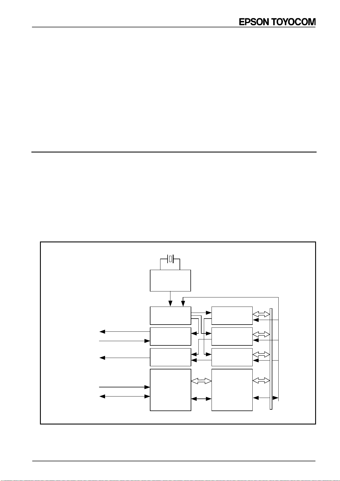
1. Overview
2. Block Diagram
2
C-Bus's high speed mode (400 kHz)
(Seconds, minutes)
(FOE and FOUT pins)
(from 2000 to 2099)
μA / 3 V (Typ.)
This module is an I2C bus interface-compliant real-time clock which includes a 32.768 kHz DTCXO.
In addition to providing a calendar (year, month, date, day, hour, minute, second) function and a clock counter
function, this module provides an abundance of other functions including an alarm function, fixed-cycle timer
function, time update interrupt function, and 32.768 kHz output function.
The devices in this module are fabricated via a C-MOS process for low current consumption, which enables
long-term battery back-up.
All of these many functions are implemented in SOP-14 pin and VSOJ-20 pin package.
The I2C-BUS is a trademark of NXP Semiconductors.
FOUT
FOE
/ INT
SCL
SDA
32kHz
DTCXO
DIVIDER
FOUT
CONTROLLER
INTERRUPT
CONTROLLER
I2C-BUS
INTERFACE
CIRCUIT
32.768 kHz
CLOCK
and
CALENDAR
TIMER
REGISTER
ALARM
REGISTER
CONTROL
REGISTER
and
SYSTEM
CONTROLLER
Page - 1 ETM26E-03
Page 5
RX − 8801 SA / JE
.
.
.
.
.
.
.
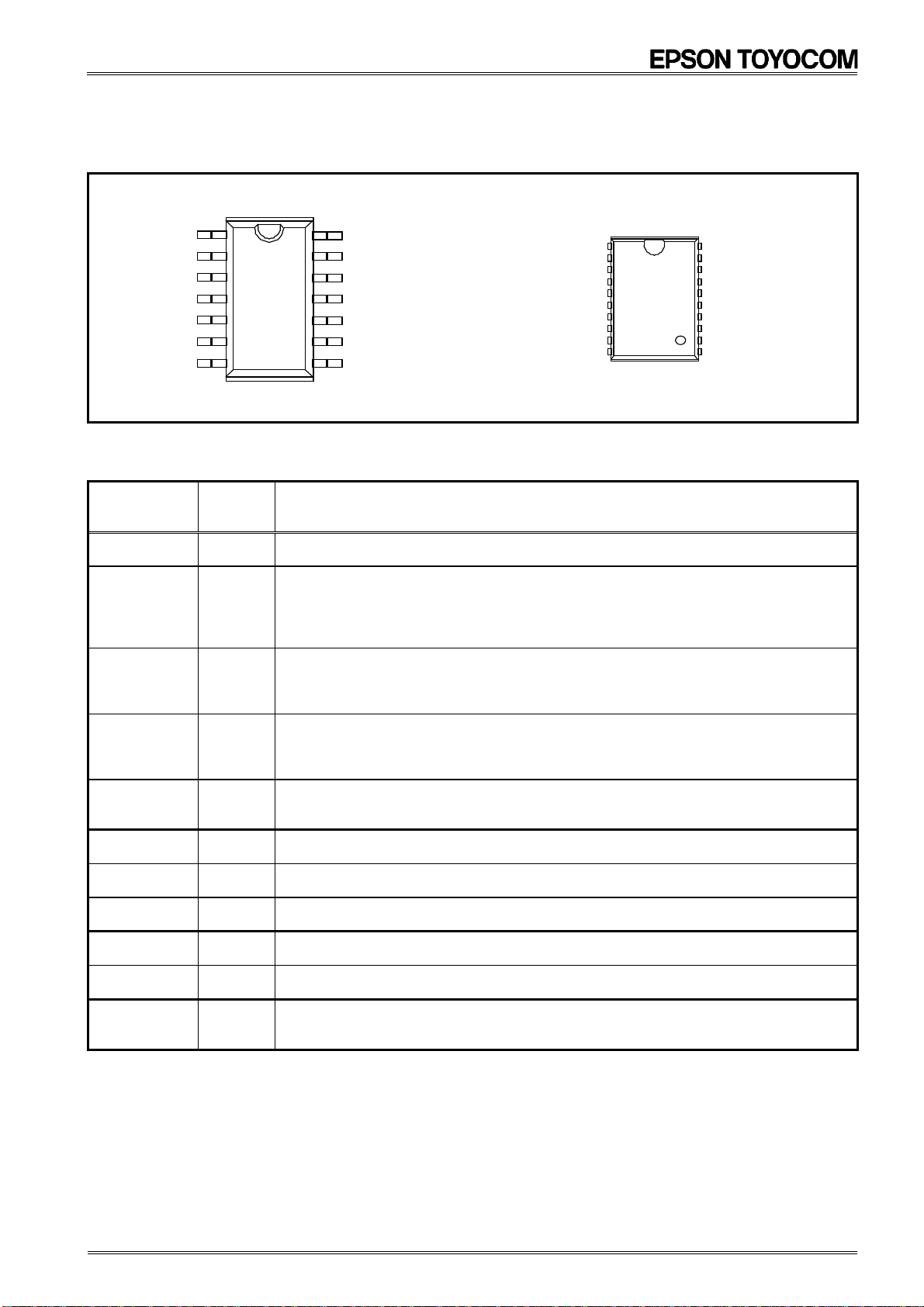
3. Terminal description
3.1. Terminal connections
T1 (CE) 14. N.C.
1
2
SCL 13. SDA
FOUT 12. T2 (VPP)
3
N.C. 11. GND
4
TEST 10. / INT
5
6
VDD 9. N. C.
FOE
7
SOP − 14pin
RX − 8801 SA
3.2. Pin Functions
Signal
name
I/O Function
SCL Input This is the serial clock input pin for I2C Bus communications.
This pin's signal is used for input and output of address, data, and ACK bits, synchronized
SDA I/O
with the serial clock used for I2C communications.
Since the SDA pin is an N-ch open drain pin during output, be sure to connect a suitable
pull-up resistance relative to the signal line capacity.
This is the C-MOS output pin with output control provided via the FOE pin.
FOUT Output
When FOE = "H" (high level), this pin outputs a 32.768 kHz signal.
When output is stopped, the FOUT pin = "Hi-Z"( high impedance ).
This is an input pin used to control the output mode of the FOUT pin.
FOE Input
When this pin's level is high, the FOUT pin is in output mode. When it is low, output via the
FOUT pin is stopped.
/ INT Output
This pins is used to output alarm signals, timer signals, time update signals, and other
signals. This pin is an open drain pin.
TEST Input * Use by the manufacture for testing. ( Do not connect externally.)
T1 (CE) Input * Use by the manufacture for testing. ( Do not connect externally.)
T2 (VPP)
VDD
GND
N.C.
−
−
−
−
* Use by the manufacture for testing. ( Do not connect externally.)
This pin is connected to a positive power supply.
This pin is connected to a ground.
This pin is not connected to the internal IC.
Leave N.C. pins open or connect them to GND or V
Note: Be sure to connect a bypass capacitor rated at least 0.1 μF between VDD and GND.
8. N.C.
10. FOE
1. /INT 20. N.C.
2. GND 19. N.C.
3. T2
(VPP) 18. N. C.
4. SDA 17. N. C.
5. N.C. 16. N.C.
6. T 1 (CE) 15. N. C.
7. SCL 14. N.C.
8. FOUT 13. N.C.
9. N.C. 12. N.C.
VSOJ − 20pin
RX − 880 1 JE
# 1
# 10
DD.
# 20
# 11
11. V
DD
Page - 2 ETM26E-03
Page 6
RX − 8801 SA / JE
4. Absolute Maximum Ratings
Item Symbol Condition Rating Unit
Supply voltage VDD Between VDD and GND
Input voltage (1) VIN1 FOE pin
Input voltage (2) VIN2 SCL and SDA pins
Output voltage (1) VOUT1 FOUT pin
Output voltage (2) VOUT2 SDA and /INT pins
Storage temperature TSTG
When stored separately,
without packaging
GND−0.3
GND−0.3
GND−0.3
GND−0.3
to +6.5 V
−0.3
to VDD+0.3 V
to +6.5 V
to VDD+0.3 V
to +6.5 V
to +125
−55
5. Recommended Operating Conditions
Item Symbol Condition Min. Typ. Max. Unit
Operating supply voltage VDD Interface voltage 1.6 3.0 5.5 V
Temp. compensation
voltage
VTEM
Clock supply voltage VCLK
Operating temperature TOPR No condensation
6. Frequency Characteristics
Item Symbol Condition Rating Unit
Frequency stability
Δ f / f
Temperature compensation
voltage
−
U A
U B
Ta= 0 to +40 °C, VDD=3.0 V
Ta=−40 to +85 °C, V
Ta= 0 to +50 °C, VDD=3.0 V
Ta=−40 to +85 °C, V
2.2 3.0 5.5 V
1.6 3.0 5.5 V
−40
DD=3.0 V
DD=3.0 V
+25 +85
(∗1)
± 1.9
± 3.4
± 3.8
± 5.0
(∗2)
(∗3)
(∗4)
GND = 0 V
°C
GND = 0 V
°C
GND = 0 V
× 10−6
Frequency/voltage
characteristics
f / V
Oscillation start time
tSTA
Aging fa
1 )
*
Equivalent to 5 seconds of month deviation. *
3 )
Equivalent to 10 seconds of month deviation. *
*
Ta= +25 °C, V
Ta= +25 °C, V
Ta=−40 to +85 °C, V
Ta= +25 °C, V
2 )
Equivalent to 9 seconds of month deviation.
4 )
Equivalent to 13 seconds of month deviation.
DD=2.2 V to 5.5 V ± 1.0 Max. × 10
DD=1.6 V
DD=1.6 V to 5.5 V
DD=3.0 V, first year ± 3 Max. × 10
1.0 Max.
3.0 Max.
−6
/ V
s
−6
/ year
Page - 3 ETM26E-03
Page 7
RX − 8801 SA / JE
A
7. Electrical Characteristics
7.1. DC Characteristics
Item Symbol Condition Min. Typ. Max. Unit
Current
consumption (1)
Current
consumption (2)
Current
consumption (3)
Current
consumption (4)
Current
consumption (5)
Current
consumption (6)
Current
consumption (7)
Current
consumption (8)
Current
consumption (9)
Current
consumption (10)
High-level input
voltage
voltage
High-level output
voltage
I
DD1
I
DD2
IDD3
IDD4
DD5
I
IDD6
IDD7
IDD8
IDD9
IDD10
VIH
VIL
VOH1
VOH2
VOH3
VOL1 VDD=5 V, IOL=1 mA GND GND+0.5
VOL2 VDD=3 V, IOL=1 mA GND GND+0.8
Low-level output
voltage
VOL3
VOL4 VDD=5 V, IOL=1 mA GND GND+0.25
VOL5
V
OL6 SDA pin
Input leakage
current
Output leakage
current
I
LK FOE, SCL, SDA pins , VIN = VDD or GND
I
OZ / INT, SDA, FOUT pins, VOUT = VDD or GND
• Temperature compensation and consumption current
SCL = 0 Hz, / INT = VDD
f
FOE = GND
FOUT : output OFF ( High Z )
Compensation interval 2.0 s
SCL = 0 Hz, / INT = VDD
f
FOE = VDD
FOUT :32.768 kHz, CL =0pF
Compensation interval 2.0 s
SCL = 0 Hz, / INT = VDD
f
FOE = VDD
FOUT :32.768 kHz, CL =30pF
Compensation interval 2.0 s
f
SCL = 0 Hz, / INT = VDD
FOE = GND
FOUT : output OFF ( High Z )
Compensation OFF
f
SCL = 0 Hz, / INT = VDD
FOE = GND
FOUT : output OFF ( High Z )
Compensation ON ( peak )
FOE pin
SCL and SDA pins
FOE pin
SCL and SDA pins
FOUT pin
FOUT pin
/ INT pin
*Unless otherwise specified, GND = 0 V, VDD = 1.6 V to 5.5 V, Ta = −40 °C to +85 °C
VDD=5 V, IOH=−1 mA
VDD=3 V, IOH=−1 mA
VDD=3 V, IOH=−100 μA
VDD=3 V, IOL=100 μA
VDD=3 V, IOL=1 mA GND GND+0.4
VDD ≥2 V, IOL=3 mA
VDD = 5 V
VDD = 3 V
V
DD = 5 V
V
DD = 3 V
V
DD = 5 V
V
DD = 3 V
V
DD = 5 V
DD = 3 V
V
V
DD = 5 V
DD = 3 V
V
0.8 × VDD
0.7 × VDD
GND − 0.3
GND − 0.3
1.2 3.4
μA
0.8 2.1
3.0 7.5
μA
2.0 5.0
8.0 20.0
μA
5.0 12.0
1.15 2.95
μA
0.72 1.85
430 900
μA
180 350
VDD + 0.3
5.5
0.2 × VDDLow-level input
0.3 × VDD
V
V
4.5 5.0
2.2 3.0
V
2.9 3.0
V
GND GND+0.1
V
GND GND+0.4 V
−0.5
−0.5
0.5
0.5
μA
μA
Compensation ON
0.977 ms
IDD9,10
verage
IDD7,8
Compensation OFF
Compensation interval ( 2.0 s )
Page - 4 ETM26E-03
IDD1,2
Page 8
RX − 8801 SA / JE
t
A
t
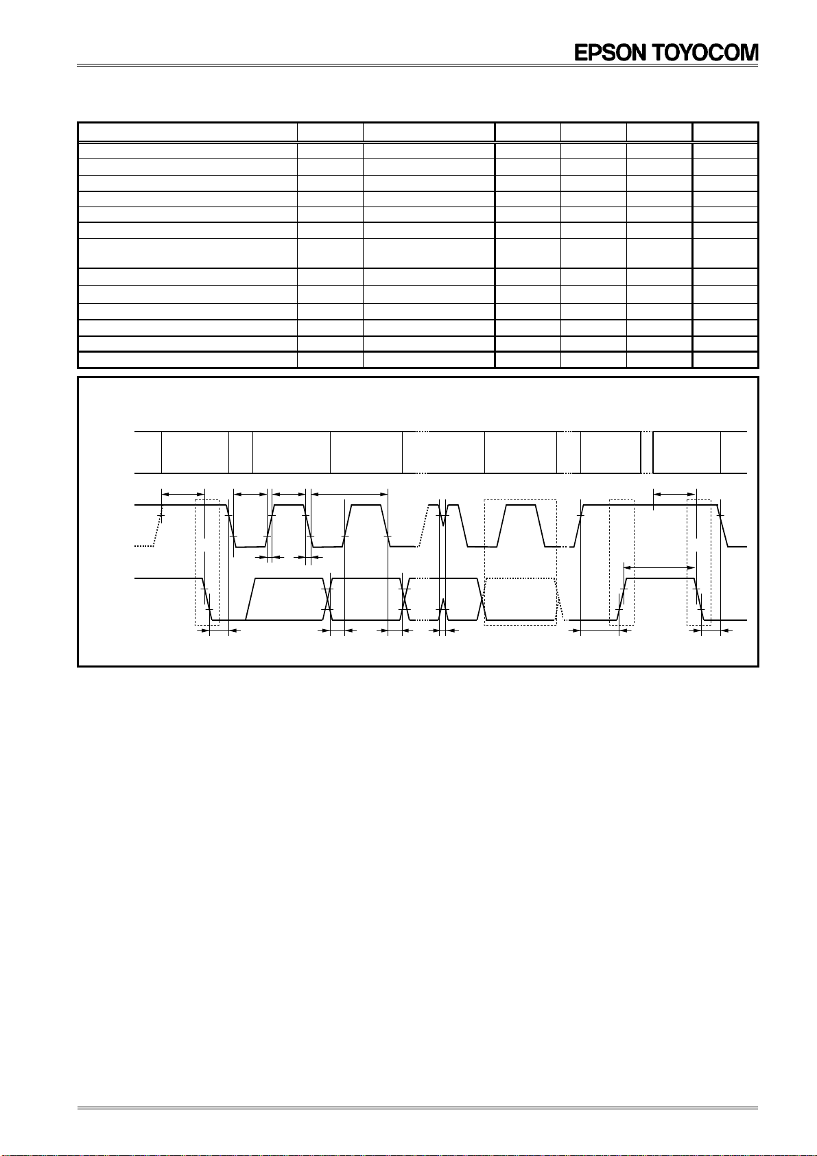
7.2. AC Characteristics
GND = 0 V , V
DD = 1.8 V to 5.5 V , Ta = −40 °C to +85 °C
Item Symbol Condition Min. Typ. Max. Unit
SCL clock frequency fSCL 400 kHz
Start condition setup time tSU;STA 0.6
Start condition hold time tHD;STA 0.6
Data setup time tSU;DAT 100 ns
Data hold time tHD;DAT 0 900 ns
Stop condition setup time tSU;STO 0.6
Bus idle time between
start condition and stop condition
Time when SCL = "L"
Time when SCL = "H"
Rise time for SCL and SDA tr 0.3
Fall time for SCL and SDA tf 0.3
Allowable spike time on bus tSP 50 ns
FOUT duty tW /t 50% of VDD level 40 50 60 %
Timing chart
START
Protocol
CONDITION
(S)
SU ; STA
tLOW tHIGH 1 / fSCL
t
BUF 1.3
t
LOW 1.3
t
HIGH 0.6
BIT 7
MSB
(A7)
BIT 6
(A6)
BIT 0
LSB
(R/W)
ACK
(A)
* Unless otherwise specified,
μs
μs
μs
μs
μs
μs
μs
μs
STOP
CONDITION
(P)
START
CONDITION
(S)
SU ; STA
SCL
(S)
(P)
t
t
r
f
t
BUF
(S)
SD
(A)
t
HD ; STA
t
SU ; DAT
t
HD ; DAT
t
SP
t
SU ; STO
t
HD ; STA
Caution: When accessing this device, all communication from transmitting the start condition to transmitting the stop
condition after access should be completed within 0.95 seconds.
If such communication requires 0.95 seconds or longer, the I
2
C bus interface is reset by the internal bus
timeout function.
Page - 5 ETM26E-03
Page 9

RX − 8801 SA / JE
8. Use Methods
8.1. Overview of Functions
1) Clock functions
This function is used to set and read out month, day, hour, date, minute, second, and year (last two digits) data.
Any (two-digit) year that is a multiple of 4 is treated as a leap year and calculated automatically as such until the year
2099.
2) Fixed-cycle interrupt generation function
The fixed-cycle timer interrupt generation function generates an interrupt event periodically at any fixed cycle set
between 244.14 μs and 4095 minutes.
When an interrupt event is generated, the /INT pin goes to low level ("L") and "1" is set to the TF bit to report that an
event has occurred. (However, when a fixed-cycle timer interrupt event has been generated, low-level output from the
/INT pin occurs only when the value of the control register's TIE bit is "1". Up to 7.8 ms after the interrupt occurs, the
/INT status is automatically cleared (/INT status changes from low level to Hi-Z).
3) Time update interrupt function
The time update interrupt function generates interrupt events at one-second or one-minute intervals, according to the
timing of the internal clock.
When an interrupt event occurs, the UF bit value becomes "1" and the /INT pin goes to low level to indicate that an
event has occurred. (However, when a fixed-cycle timer interrupt event has been generated, low-level output from the
/INT pin occurs only when the value of the control register's UIE bit is "1". This /INT status is automatically cleared
(/INT status changes from low level to Hi-Z) 7.8 ms (a fixed value) after the interrupt occurs.
4) Alarm interrupt function
The alarm interrupt generation function generates interrupt events for alarm settings such as date, day, hour, and
minute settings.
When an interrupt event occurs, the AF bit value is set to "1" and the /INT pin goes to low level to indicate that an event
has occurred.
5) 32.768-kHz clock output
The 32.768-kHz clock (with precision equal to that of the built-in crystal oscillator) can be output via the FOUT pin.
The FOUT pin is a CMOS output pin which can be set for clock output when the FOE pin is at high level and for
low-level output when the FOE pin is at high impedance.
6) Interface with CPU
Data is read and written via the I2C bus interface using two signal lines: SCL (clock) and SDA (data).
Since neither SCL nor SDA includes a protective diode on the V
supply voltages can still be implemented by adding pull-up resistors to the circuit board.
The SCL's maximum clock frequency is 400 kHz (when V
DD side, a data interface between hosts with differing
DD ≥ 1.8 V), which supports the I
2
C bus's high-speed mode.
Page - 6 ETM26E-03
Page 10
RX − 8801 SA / JE
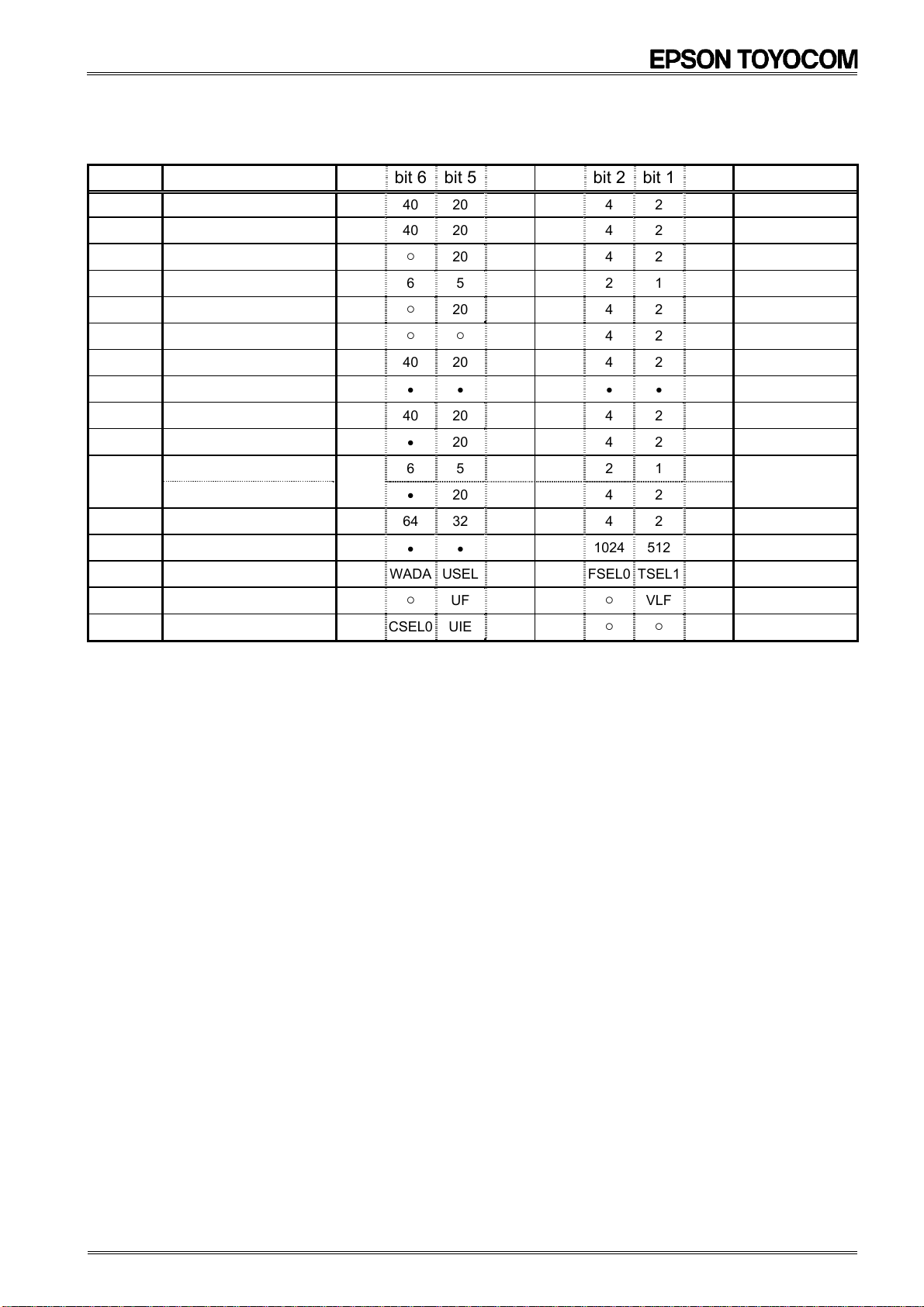
8.2. Description of Registers
8.2.1. Register table
Address Function bit 7 bit 6 bit 5 bit 4 bit 3 bit 2 bit 1 bit 0
0 SEC
1 MIN
2 HOUR
3 WEEK
4 DAY
5 MONTH
6 YEAR 80 40 20 10 8 4 2 1
7 RAM
8 MIN Alarm AE 40 20 10 8 4 2 1
9 HOUR Alarm AE
WEEK Alarm 6 5 4 3 2 1 0
A
DAY Alarm
B Timer Counter 0 128 64 32 16 8 4 2 1
C Timer Counter 1
D Extension Register TEST WADA USEL TE FSEL1 FSEL0 TSEL1 TSEL0
E Flag Register
F Control Register CSEL1 CSEL0 UIE TIE AIE
Note
When after the initial power-up or when the result of read out the VLF bit is "1" , initialize all registers, before
using the module.
Be sure to avoid entering incorrect date and time data, as clock operations are not guaranteed when the data or
time data is incorrect.
∗1) During the initial power-up, the TEST bit is reset to "0" and the VLF bit is set to "1".
∗ At this point, all other register values are undefined, so be sure to perform a reset before using the module.
Only a "0" can be written to the UF, TF, AF, or VLF bit.
∗2)
Any bit marked with "{" should be used with a value of "0" after initialization.
∗3)
∗4) Any bit marked with "•" is a RAM bit that can be used to read or write any data.
The TEST bit is used by the manufacturer for testing. Be sure to set "0" for this bit when writing.
∗5)
{
40 20 10 8 4 2 1
{
40 20 10 8 4 2 1
{ {
{
{ {
{ { {
6 5 4 3 2 1 0
20 10 8 4 2 1
20 10 8 4 2 1
10 8 4 2 1
• • • • • • • •
20 10 8 4 2 1
•
AE
20 10 8 4 2 1
•
• • • •
{ {
UF TF AF
2048 1024 512 256
{
VLF VDET
{ {
RESET
Remark
∗3
∗3
∗3
∗3
∗3
∗3
−
∗4
−
∗4
∗4
−
∗4
∗1, ∗3, ∗5
∗1, ∗2, ∗3
∗3
Page - 7 ETM26E-03
Page 11
RX − 8801 SA / JE
8.2.2. Control register (Reg F)
Address Function bit 7 bit 6 bit 5 bit 4 bit 3 bit 2 bit 1 bit 0
F
∗1) The default value is the value that is read (or is set internally) after powering up from 0 V.
∗2) "o" indicates write-protected bits. A zero is always read from these bits.
∗3) "−" indicates no default value has been defined.
• This register is used to control interrupt event output from the /INT pin and the stop/start status of clock and
calendar operations.
1) CSEL0,1 ( Compensation interval Select 0, 1 ) bits
The combination of these two bits is used to set the temperature compensation interval.
2) UIE ( Update Interrupt Enable ) bit
When a time update interrupt event is generated (when the UF bit value changes from "0" to "1"), this bit's value
specifies if an interrupt signal is generated (/INT status changes from Hi-Z to low) or is not generated (/INT status
remains Hi-Z).
When a "1" is written to this bit, an interrupt signal is generated (/INT status changes from Hi-Z to low) when an
interrupt event is generated.
When a "0" is written to this bit, no interrupt signal is generated when an interrupt event occurs.
Control Register CSEL1 CSEL0 UIE TIE AIE
CSEL0,1
Write/Read
UIE
(Default) (0) (1)
CSEL1
(bit 7)
CSEL0
(bit 6)
(−) (−) (−)
Compensation interval
{ {
(0) (0)
0 0 0.5 s
0 1 2.0 s
∗ Default
1 0 10 s
1 1 30 s
Data Function
RESET
(−)
When a time update interrupt event occurs, an interrupt signal is not
generated or is canceled (/INT status changes from low to Hi-Z).
When a time update interrupt event occurs, an interrupt signal is generated
(/INT status changes from Hi-Z to low).
When a time update interrupt event occurs, low-level output from the /INT pin occurs only when
∗
the value of the control register's UIE bit is "1". This /INT status is automatically cleared (/INT
status changes from low to Hi-Z) 7.8 ms after the interrupt occurs.
Write/Read
0
1
2) TIE ( Timer Interrupt Enable ) bit
When a fixed-cycle timer interrupt event occurs (when the TF bit value changes from "0" to "1"), this bit's value
specifies if an interrupt signal is generated (/INT status changes from Hi-Z to low) or is not generated (/INT status
remains Hi-Z).
When a "1" is written to this bit, an interrupt signal is generated (/INT status changes from Hi-Z to low) when an
interrupt event is generated.
When a "0" is written to this bit, no interrupt signal is generated when an interrupt event occurs.
TIE
Write/Read
Data Function
0
When a fixed-cycle timer interrupt event occurs, an interrupt signal is not
generated or is canceled (/INT status changes from low to Hi-Z).
When a fixed-cycle timer interrupt event occurs, an interrupt signal is
generated (/INT status changes from Hi-Z to low).
1
* When a fixed-cycle timer interrupt event has been generated low-level output from the /INT pin
occurs only when the value of the control register's TIE bit is "1". Up to 7.8 ms after the interrupt
occurs, the /INT status is automatically cleared (/INT status changes from low to Hi-Z)
.
Page - 8 ETM26E-03
Page 12

RX − 8801 SA / JE
3) AIE ( Alarm Interrupt Enable ) bit
When an alarm timer interrupt event occurs (when the AF bit value changes from "0" to "1"), this bit's value
specifies if an interrupt signal is generated (/INT status changes from Hi-Z to low) or is not generated (/INT status
remains Hi-Z).
When a "1" is written to this bit, an interrupt signal is generated (/INT status changes from Hi-Z to low) when an
interrupt event is generated.
When a "0" is written to this bit, no interrupt signal is generated when an interrupt event occurs.
AIE
Data Function
0
Write/Read
1
∗ For details, see "8.5. Alarm Interrupt Function".
[Caution]
(1) The /INT pin is a shared interrupt output pin for three types of interrupts. It outputs the OR'ed result of these interrupt outputs.
When an interrupt has occurred (when the /INT pin is at low level), the UF, TF, read AF flags to determine which flag has a value of "1"
(this indicates which type of interrupt event has occurred).
(2) To keep the /INT pin from changing to low level, write "0" to the UIE, TIE, and AIE bits. To check whether an event has occurred without
outputting any interrupts via the /INT pin, use software to monitor the value of the UF, TF, and AF interrupt flags.
When an alarm interrupt event occurs, an interrupt signal is not generated
or is canceled (/INT status changes from low to Hi-Z).
When an alarm interrupt event occurs, an interrupt signal is generated (/INT
status changes from Hi-Z to low).
∗
When an alarm interrupt event has been generated low-level output from the /INT pin occurs
only when the value of the control register's AIE bit is "1". This setting is retained until the AF
bit value is cleared to zero. (No automatic cancellation)
4) RESET bit
It also resets the RTC module's internal counter value when the value is less than one second.
Writing a "1" to this bit stops the counter operation and resets the RTC module's internal counter value when the
value is less than one second.
If a STOP-condition or repeated START-condition(I
operating, stop status is automatically canceled (the RESET bit value is changed from "1" to "0").
∗ For optimum performance, do not use this bit for functions other than the clock and calendar functions.
RESET
Data Description
[Normal operation mode]
This bit is used to cancel stop status for (i.e., restart) the clock and calendar
0
function. Also, when "1" is written to the RESET bit, it cancels stop status for
the fixed-cycle timer function.
∗
Since operation is not restarted when the STOP bit value is "1", to restart operation, a "0" must
be written to both the STOP bit and the RESET bit.
[Operation stop mode]
Stops updating of year, month, date, day, hour, minute, and second values
and partially stops the fixed-cycle timer function.
(Stop 1) Stops updating of year, month, date, day, hour, minute, and
Write/Read
second values
• This stops all clock and calendar update operations.
Once this occurs, no more time update interrupt events or alarm
1
interrupt events occur.
(Stop 2) Partially stops the fixed-cycle timer function
• If the fixed-cycle timer's source clock settings include an update
setting of 64 Hz, 1 Hz, or "Minute", the fixed-cycle timer function does
not operate.
∗ However, this function does operate when the fixed-cycle timer's source clock setting is
4096 Hz.
(Note) When this bit value is "1", the internal divider keeps the reset state, from 2048Hz to 1
Hz .
2
C) is received while the 0.95-second bus timeout function is
Page - 9 ETM26E-03
Page 13

RX − 8801 SA / JE
8.2.3. Flag register (Reg-E)
Address Function bit 7 bit 6 bit 5 bit 4 bit 3 bit 2 bit 1 bit 0
E
∗1) The default value is the value that is read (or is set internally) after powering up from 0 V.
∗2) "o" indicates write-protected bits. A zero is always read from these bits.
∗3) "−" indicates a default value is undefined.
• This register is used to detect the occurrence of various interrupt events and reliability problems in internal data.
1) UF ( Update Flag ) bit
If set to "0" beforehand, this flag bit's value changes from "0" to 1" when a time update interrupt event has
occurred. Once this flag bit's value is "1", its value is retained until a "0" is written to it.
∗
For details, see "8.4. Time Update Interrupt Function".
2) TF ( Timer Flag ) bit
If set to "0" beforehand, this flag bit's value changes from "0" to 1" when a fixed-cycle timer interrupt event has
occurred. Once this flag bit's value is "1", its value is retained until a "0" is written to it.
∗
For details, see "8.3. Fixed-cycle Timer Interrupt Function".
3) AF ( Alarm Flag ) bit
If set to "0" beforehand, this flag bit's value changes from "0" to 1" when an alarm interrupt event has occurred.
Once this flag bit's value is "1", its value is retained until a "0" is written to it.
∗
For details, see "8.5. Alarm Interrupt Function".
4) VLF ( Voltage Low Flag ) bit
This flag bit indicates the retained status of clock operations or internal data. Its value changes from "0" to "1"
when data loss occurs, such as due to a supply voltage drop. Once this flag bit's value is "1", its value is retained
until a "0" is written to it.
When after powering up from 0 V this bit's value is "1" .
Flag register
VLF
(Default) (0) (0)
{ {
UF TF AF
(−) (−) (−)
{
(0) (1) (1)
VLF VDET
Data Description
0 The VLF bit is cleared to zero to prepare for the next status detection.
Write
1 This bit is invalid after a "1" has been written to it.
0
Read
1
Data loss is not detected.
Data loss is detected. All registers must be initialized.
( This setting is retained until a "zero" is written to this bit. )
5) VDET ( Voltage Detection Flag ) bit
This flag bit indicates the status of temperature compensation. Its value changes from "0" to "1" when stop the
temperature compensation, such as due to a supply voltage drop. Once this flag bit's value is "1", its value is
retained until a "0" is written to it.
When after powering up from 0 V this bit's value is "1" .
VDET
Data Description
0 The VDET bit is cleared to zero to prepare for the next low voltage detection.
Write
1 The write access of "1" to this bit is invalid.
0
Temperature compensation is normal.
Read
1
Temperature compensation is stop detected.
Page - 10 ETM26E-03
Page 14

RX − 8801 SA / JE
8.2.4. Extension register (Reg-D)
Address Function bit 7 bit 6 bit 5 bit 4 bit 3 bit 2 bit 1 bit 0
D
∗1) The default value is the value that is read (or is set internally) after powering up from 0 V.
∗2) "o" indicates write-protected bits. A zero is always read from these bits.
∗3) "−" indicates a default value is undefined.
• This register is used to specify the target for the alarm function or time update interrupt function and to select or set
operations such as fixed-cycle timer operations.
1) TEST bit
This is the manufacturer's test bit. Its value should always be "0".
Be careful to avoid writing a "1" to this bit when writing to other bits.
∗
If a "1" is inadvertently written to this TEST bit, there is a safety function where by this bit will be automatically cleared to zero when a STOP
condition or Repeated START condition is received or when the 0.95-second bus timeout function operates.
Extension Register TEST WADA USEL TE FSEL1 FSEL0 TSEL1 TSEL0
(Default) (0)
TEST
(−) (−) (−)
(0) (0)
(−) (−)
Data Description
0 Normal operation mode
∗ Default
Write/Read
1 Setting prohibited (manufacturer's test bit)
2) WADA ( Week Alarm/Day Alarm ) bit
This bit is used to specify either WEEK or DAY as the target of the alarm interrupt function.
Writing a "1" to this bit specifies DAY as the comparison object for the alarm interrupt function.
Writing a "0" to this bit specifies WEEK as the comparison object for the alarm interrupt function.
3) USEL ( Update Interrupt Select ) bit
This bit is used to specify either "second update" or "minute update" as the update generation timing of the time
update interrupt function.
USEL
Write/Read
Data update interrupts
0 second update ∗ Default 500 ms
Auto reset time
t
RTN
1 minute update 7.813 ms
4) TE ( Timer Enable ) bit
This bit controls the start/stop setting for the fixed-cycle timer interrupt function.
Writing a "1" to this bit specifies starting of the fixed-cycle timer interrupt function (a countdown starts from a
preset value).
Writing a "0" to this bit specifies stopping of the fixed-cycle timer interrupt function.
5) FSEL0,1 ( FOUT frequency Select 0, 1 ) bits
The combination of these two bits is used to set the FOUT frequency.
FSEL0,1
Write/Read
FSEL1
(bit 3)
0 0
0 1
1 0
1 1
FSEL0
(bit 2)
FOUT frequency
32768 Hz Output
1024 Hz Output
1 Hz Output
32768 Hz Output
∗ Default
6) TSEL0,1 ( Timer Select 0, 1 ) bits
The combination of these two bits is used to set the countdown period (source clock) for the fixed-cycle timer
interrupt function (four settings can be made).
TSEL0,1
Write/Read
TSEL1
(bit 1)
0 0 4096 Hz
0 1 64 Hz / Once per 15.625 ms
TSEL0
(bit 0)
Source clock
/Once per 244.14 μs
1 0 "Second" update /Once per second
1 1 "Minute" update /Once per minute
Page - 11 ETM26E-03
Page 15

RX − 8801 SA / JE
8.2.5. RAM register (Reg - 7)
Address Function bit 7 bit 6 bit 5 bit 4 bit 3 bit 2 bit 1 bit 0
7 RAM
• This RAM register is read/write accessible for any data in the range from 00 h to FF h.
8.2.6. Clock counter (Reg - 0 ∼ 2)
Address Function bit 7 bit 6 bit 5 bit 4 bit 3 bit 2 bit 1 bit 0
0 SEC
1 MIN
2 HOUR
∗) "o" indicates write-protected bits. A zero is always read from these bits.
• The clock counter counts seconds, minutes, and hours.
• The data format is BCD format
seconds.
∗ Note with caution that writing non-existent time data may interfere with normal operation of the clock counter.
1) Second counter
Address Function bit 7 bit 6 bit 5 bit 4 bit 3 bit 2 bit 1 bit 0
0 SEC
• This second counter counts from "00" to "01," "02," and up to 59 seconds, after which it starts again from
00 seconds.
2) Minute counter
3) Hour counter
8.2.7. Day counter (Reg - 3)
∗) "o" indicates write-protected bits. A zero is always read from these bits.
Address Function bit 7 bit 6 bit 5 bit 4 bit 3 bit 2 bit 1 bit 0
1 MIN
• This minute counter counts from "00" to "01," "02," and up to 59 minutes, after which it starts again from
00 minutes.
Address Function bit 7 bit 6 bit 5 bit 4 bit 3 bit 2 bit 1 bit 0
2 HOUR
• This hour counter counts from "00" hours to "01," "02," and up to 23 hours, after which it starts again from
00 hours.
Address Function bit 7 bit 6 bit 5 bit 4 bit 3 bit 2 bit 1 bit 0
3 WEEK
• The day (of the week) is indicated by 7 bits, bit 0 to bit 6.
The day data values are counted as: Day 01h → Day 02h → Day 04h → Day 08h → Day 10h → Day
20h → Day 40h → Day 01h → Day 02h, etc.
• The correspondence between days and count values is shown below.
WEEK bit 7 bit 6 bit 5 bit 4 bit 3 bit 2 bit 1 bit 0 Day Data [h]
Write/Read
Write prohibit
• • • • • • • •
{
{
{ {
. For example, when the "seconds" register value is "0101 1001" it indicates 59
{
{
{ {
{
0 0 0 0 0 0 0
0 0 0 0 0 0
0 0 0 0 0
0 0 0 0
0 0 0
0 0
0
1
40 20 10 8 4 2 1
40 20 10 8 4 2 1
20 10 8 4 2 1
40 20 10 8 4 2 1
40 20 10 8 4 2 1
20 10 8 4 2 1
6 5 4 3 2 1 0
1
1
1
1
1
1
0 0 0 0 0 Friday 20 h
0 0 0 0 Thursday 10 h
0 0 0 Wednesday 08 h
0 0 Tuesday 04 h
0 Monday 02 h
Sunday 01 h
0 0 0 0 0 0 Saturday 40 h
∗ Do not set "1" to more than one day at the same time.
Also, note with caution that any setting other than the
seven shown above should not be made as it may
− −
interfere with normal operation.
Page - 12 ETM26E-03
Page 16

RX − 8801 SA / JE
8.2.8. Calendar counter (Reg 4 to 6)
Address Function bit 7 bit 6 bit 5 bit 4 bit 3 bit 2 bit 1 bit 0
4 DAY
5 MONTH
6 YEAR 80 40 20 10 8 4 2 1
∗) "o" indicates write-protected bits. A zero is always read from these bits.
• The auto calendar function updates all dates, months, and years from January 1, 2001 to December 31, 2099.
• The data format is BCD format. For example, a date register value of "0011 0001" indicates the 31st.
∗ Note with caution that writing non-existent date data may interfere with normal operation of the calendar counter.
1) Date counter
Address Function bit 7 bit 6 bit 5 bit 4 bit 3 bit 2 bit 1 bit 0
4 DAY
• The updating of dates by the date counter varies according to the month setting.
∗ A leap year is set whenever the year value is a multiple of four (such as 04, 08, 12, 88, 92, or 96). In
February of a leap year, the counter counts dates from "01," "02," "03," to "28," "29," "01," etc.
DAY Month Date update pattern
Write/Read
2) Month counter
Address Function bit 7 bit 6 bit 5 bit 4 bit 3 bit 2 bit 1 bit 0
5 MONTH
• The month counter counts from 01 (January), 02 (February), and up to 12 (December), then starts again at
01 (January).
3) Year counter
Address Function bit 7 bit 6 bit 5 bit 4 bit 3 bit 2 bit 1 bit 0
6 Years Y80 Y40 Y20 Y10 Y8 Y4 Y2 Y1
• The year counter counts from 00, 01, 02 and up to 99, then starts again at 00.
• Any year that is a multiple of four (04, 08, 12, 88, 92, 96, etc.) is handled as a leap year.
8.2.9. Alarm registers (Reg - 8 ∼ A)
Address Function bit 7 bit 6 bit 5 bit 4 bit 3 bit 2 bit 1 bit 0
8 MIN Alarm AE 40 20 10 8 4 2 1
9 HOUR Alarm AE
A
WEEK Alarm 6 5 4 3 2 1 0
DAY Alarm
• The alarm interrupt function is used, along with the AEI, AF, and WADA bits, to set alarms for specified date, day,
hour, and minute values.
• When the settings in the above alarm registers and the WADA bit match the current time, the /INT pin goes to low
level and "1" is set to the AF bit to report that and alarm interrupt event has occurred.
8.2.10. Fixed-cycle timer control registers (Reg - B to C)
Address Function bit 7 bit 6 bit 5 bit 4 bit 3 bit 2 bit 1 bit 0
B Timer Counter 0 128 64 32 16 8 4 2 1
C Timer Counter 1
• These registers are used to set the preset countdown value for the fixed-cycle timer interrupt function.
The TE, TF, TIE, and TSEL0/1 bits are also used to set the fixed-cycle timer interrupt function.
• When the value in the above fixed-cycle timer control register changes from 001h to 000h, the /INT pin goes to low
level and "1" is set to the TF bit to report that a fixed-cycle timer interrupt event has occurred.
{ {
{ { {
{ {
1, 3, 5, 7, 8, 10, or 12
4, 6, 9, or 11
February in normal year
February in leap year
{ { {
AE
• • • •
20 10 8 4 2 1
10 8 4 2 1
20 10 8 4 2 1
01, 02, 03 ∼ 30, 31, 01 ∼
01, 02, 03 ∼ 30, 01, 02 ∼
01, 02, 03 ∼ 28, 01, 02 ∼
01, 02, 03 ∼ 28, 29, 01 ∼
10 8 4 2 1
•
•
20 10 8 4 2 1
20 10 8 4 2 1
2048 1024 512 256
Page - 13 ETM26E-03
Page 17

RX − 8801 SA / JE
" 1 "
p
p
p
p
" 1 " " 0 " " 1 " " 0 " Hi - z " L " " 1 " " 0 "
8.3. Fixed-cycle Timer Interrupt Function
8.3.1. Diagram of fixed-cycle timer interrupt function
The fixed-cycle timer interrupt generation function generates an interrupt event periodically at any fixed cycle set
between 244.14 μs and 4095 minutes.
When an interrupt event is generated, the /INT pin goes to low level and "1" is set to the TF bit to report that an
event has occurred. (However, when a fixed-cycle timer interrupt event has been generated low-level output from
the /INT pin occurs only when the value of the control register's TIE bit is "1". Up to 7.8 ms after the interrupt
occurs, the /INT status is automatically cleared (/INT status changes from low-level to Hi-Z).
∗ Example of
/INT operation
TIE = " 1 "
TE = " 0 "
→ " 1 "
Fixed-cycle timer starts Fixed-cycle timer stops
7.8ms
(Max.)
period
TIE =
→ " 0 "
TE bit
TIE bit
/INT output
TF bit
Event occurs
(1)
" 1 "
(5)
(3)
eriod
000 h
(2)
001 h
• • •
(1)
When the TE bit value changes from "0" to "1" the fixed-cycle timer function starts.
∗
The counter always starts counting down from the preset value when the TE value changes from "0" to "1".
RTC internal operation
Write operation
→
Operation of fixed-cycle timer
(6)
(4)
eriod
tRTNtRTN
(8)
Even when the TF
∗
bit is cleared to zero,
the /INT status does
not change.
eriod
(9)
tRTN
eriod
(7)
(7)
Even when the TE bit is
∗
tRTN
cleared to zero, /INT
remains low during the
tRTN time.
(7)
(1) When a "1" is written to the TE bit, the fixed-cycle timer countdown starts from the preset value.
(2) A fixed-cycle timer interrupt event starts a countdown based on the countdown period (source clock). When the
count value changes from 001h to 000h, an interrupt event occurs.
∗ After the interrupt event that occurs when the count value changes from 001h to 000h, the counter
automatically reloads the preset value and again starts to count down. (Repeated operation)
(3) When a fixed-cycle timer interrupt event occurs, "1" is written to the TF bit.
(4) When the TF bit = "1" its value is retained until it is cleared to zero.
(5) If the TIE bit = "1" when a fixed-cycle timer interrupt occurs, /INT pin output goes low.
∗ If the TIE bit = "0" when a fixed-cycle timer interrupt occurs, /INT pin output remains Hi-Z.
(6) Output from the /INT pin remains low during the tRTN period following each event, after which it is automatically
cleared to Hi-Z status.
∗ /INT is again set low when the next interrupt event occurs.
(7) When a "0" is written to the TE bit, the fixed-cycle timer function is stopped and the /INT pin is set to Hi-Z status.
∗ When /INT = low, the fixed-cycle timer function is stopped. The tRTN period is the maximum amount of time
before the /INT pin status changes from low to Hi-Z.
(8) As long as /INT = low, the /INT pin status does not change when the TF bit value changes from "1" to "0".
(9) When /INT = low, the /INT pin status changes from low to Hi-Z as soon as the TIE bit value changes from "1" to
"0".
Page - 14 ETM26E-03
Page 18

RX − 8801 SA / JE
8.3.2. Related registers for function of time update interrupts.
Address Function bit 7 bit 6 bit 5 bit 4 bit 3 bit 2 bit 1 bit 0
B Timer Counter 0
C Timer Counter 1
D Extension Register
E Flag Register
F Control Register
∗1) "o" indicates write-protected bits. A zero is always read from these bits.
∗2) Bits marked with "•" are RAM bits that can contain any value and are read/write-accessible.
∗ Before entering settings for operations, we recommend writing a "0" to the TE and TIE bits to prevent hardware
interrupts from occurring inadvertently while entering settings.
∗ When the STOP bit or RESET bit value is "1" the time update interrupt function operates only partially.
(Operation continues if the source clock setting is 4096 Hz. Otherwise, operation is stopped.)
∗ When the fixed-cycle timer interrupt function is not being used, the fixed-cycle timer control register (Reg – B to C)
can be used as a RAM register. In such cases, stop the fixed-cycle timer function by writing "0" to the TE and TIE
bits.
1) TSEL0,1 bits (Timer Select 0, 1)
The combination of these two bits is used to set the countdown period (source clock) for the fixed-cycle timer
interrupt function (four settings can be made).
TSEL0,1
TSEL1
(bit 1)
TSEL0
(bit 0)
0 0 4096 Hz
Write/Read
0 1 64 Hz / Once per 15.625 ms
1 0 "Second" update /Once per second
1 1 "Minute" update /Once per minute
∗1) The /INT pin's auto reset time (tRTN) varies as shown above according to the source clock setting.
∗2) When the source clock has been set to "second update" or "minute update", the timing of both
countdown and interrupts is coordinated with the clock update timing.
2) Fixed-cycle Timer Control register (Reg - B to C)
This register is used to set the default (preset) value for the counter. Any count value from 1 (001 h) to
4095 (FFFh) can be set. The counter counts down based on the source clock's period, and when the count value
changes from 001h to 000h, the TF bit value becomes "1".
The countdown that starts when the TE bit value changes from "0" to "1" always begins from the preset value.
Be sure to write "0" to the TE bit before writing the preset value. If a value is written while TE = "1" the first
subsequent event will not be generated correctly.
Address C
Timer Counter 1
bit 7 bit 6 bit 5 bit 4 bit 3 bit 2 bit 1 bit 0 bit 7 bit 6 bit 5 bit 4 bit 3 bit 2 bit 1 bit 0
• • • •
3) TE (Timer Enable) bit
This bit controls the start/stop setting for the fixed-cycle timer interrupt function.
TE
Data Description
128 64 32 16 8 4 2 1
• • • •
TEST WADA USEL
{ {
CSEL1 CSEL0 UIE
Source clock
2048 1024 512 256 128 64 32 16 8 4 2 1
TE
UF
TF
TIE
/Once per 244.14 μs
2048 1024 512 256
FSEL1 FSEL0
AF
AIE
Auto reset time
tRTN
TSEL1 TSEL0
{
{ {
VLF VDET
RESET bits
RESET
Effects of
122 μs −
7.8125 ms
7.8125 ms
7.8125 ms
∗
Does not operate
when the RESET
bit value is "1".
Address B
Timer Counter 0
0 Stops fixed-cycle timer interrupt function.
Write/Read
1
Starts fixed-cycle timer interrupt function.
The countdown that starts when the TE bit value changes from "0" to "1" always begins from the
∗
preset value.
4) TF (Timer Flag) bit
If set to "0" beforehand, this flag bit's value changes from "0" to 1" when a fixed-cycle timer interrupt event has
occurred. Once this flag bit's value is "1", its value is retained until a "0" is written to it.
TF
Write
Data Description
0
1 This bit is invalid after a "1" has been written to it.
The TF bit is cleared to zero to prepare for the next status detection
∗ Clearing this bit to zero does not enable the /INT low output status to be cleared (to Hi-Z).
0 Fixed-cycle timer interrupt events are not detected.
Read
1
Fixed-cycle timer interrupt events are detected.
(Result is retained until this bit is cleared to zero.)
Page - 15 ETM26E-03
Page 19

RX − 8801 SA / JE
A
A
5) TIE (Timer Interrupt Enable) bit
When a fixed-cycle timer interrupt event occurs (when the TF bit value changes from "0" to "1"), this bit's value
specifies whether an interrupt signal is generated (/INT status changes from Hi-Z to low) or is not generated (/INT
status remains Hi-Z).
TIE
Write/Read
8.3.3. Fixed-cycle timer interrupt interval (example)
Timer
Counter
setting
0
1
2
•
•
•
41 10.010 ms 640.63 ms 41 s 41 min
205 50.049 ms 3.203 s 205 s 205 min
410 100.10 ms 6.406 s 410 s 410 min
2048 500.00 ms 32.000 s 2048 s 2048 min
•
•
•
4095 0.9998 s 63.984 s 4095 s 4095 min
• Time error in fixed-cycle timer
A time error in the fixed-cycle timer will produce a positive or negative time period error in the selected
source clock. The fixed-cycle timer's time is within the following range relative to the time setting.
(Fixed-cycle timer's time setting (∗) − source clock period) to (timer's time setting)
∗) The timer's time setting = source clock period × timer counter's division value.
∗ The time actually set to the timer is adjusted by adding the time described above to the
communication time for the serial data transfer clock used for the setting.
8.3.4. Fixed-cycle timer start timing
Counting down of the fixed-cycle timer value starts at the rising edge of the SCL signal that occurs when the TE value
is changed from "0" to "1" (after bit 0 is transferred).
Data Description
1) When a fixed-cycle timer interrupt event occurs, an interrupt signal is not
generated or is canceled (/INT status remains Hi-Z).
0
2) When a fixed-cycle timer interrupt event occurs, the interrupt signal is
canceled (/INT status changes from low to Hi-Z).
∗
Even when the TIE bit value is "0" another interrupt event may change the /INT status to low (or
may hold /INT = "L").
When a fixed-cycle timer interrupt event occurs, an interrupt signal is
generated (/INT status changes from Hi-Z to low).
1
∗ When a fixed-cycle timer interrupt event has been generated low-level output from the /INT pin
occurs only when the value of the control register's TIE bit is "1". Up to 7.8 ms after the interrupt
occurs, the /INT status is automatically cleared (/INT status changes from low to Hi-Z).
Source clock
4096 Hz
TSEL1,0 = 0,0
64 Hz
TSEL1,0 = 0,1
"Second"
update
TSEL1,0 = 1,0
− − − −
244.14
488.28
•
•
•
•
•
•
μs
μs
15.625 ms 1 s 1 min
31.25 ms 2 s 2 min
•
•
•
•
•
•
•
•
•
•
•
•
ddress D
"Minute"
update
TSEL1,0 = 1,1
•
•
•
•
•
•
SCL pin
SDA pin
FSEL1
TE
TSEL1
TSEL0
CKFSEL0
Internal timer
/INT pin
Operation of tim er
Page - 16 ETM26E-03
Page 20

RX − 8801 SA / JE
" 1 "
p
p
p
p
" 1 " " 0 " Hi - z " L " " 1 " " 0 "
/
8.4. Time Update Interrupt Function
8.4.1. Time update interrupt function diagram
The time update interrupt function generates interrupt events at one-second or one-minute intervals, according to
the timing of the internal clock.
When an interrupt event occurs, the UF bit value becomes "1" and the /INT pin goes to low level to indicate that an
event has occurred. (However, when a fixed-cycle timer interrupt event has been generated, low-level output from
the /INT
cleared (/INT status changes from low level to Hi-Z) 7.8
pin occurs only when the value of the control register's UIE bit is "1". This /INT status is automatically
∗ /INT operation
example
UIE = " 1 "
" 1 "
7.8ms
period
ms (fixed value) after the interrupt occurs.
UIE =
(7)
→ " 0 "
eriod
(4)
(2)
(1)
(5)
eriod
(3)
tRTNtRTN
(6)
INT status does not
∗
change when UF bit is
cleared to zero.
eriod
tRTN
tRTN
eriod
UIE bit
/INT output
UF bit
Events
Operation in RTC
Write operation
(1) A time update interrupt event occurs when the internal clock's value matches either the second update time or
the minute update time. The USEL bit's specification determines whether it is the second update time or the
minute update time that must be matched.
(2) When a time update interrupt event occurs, the UF bit value becomes "1".
(3) When the UF bit value is "1" its value is retained until it is cleared to zero.
(4) When a time update interrupt occurs, /INT pin output is low if UIE = "1".
∗ If UIE = "0" when a timer update interrupt occurs, the /INT pin status remains Hi-Z.
(5) Each time an event occurs, /INT pin output is low only up to the tRTN time (which is fixed as 7.1825 ms for
time update interrupts) after which it is automatically cleared to Hi-Z.
∗ /INT pin output goes low again when the next interrupt event occurs.
(6) As long as /INT = low, the /INT pin status does not change, even if the UF bit value changes from "1" to "0".
(7) When /INT = low, the /INT pin status changes from low to Hi-Z as soon as the UIE bit value changes from "1"
to
"0".
Page - 17 ETM26E-03
Page 21

RX − 8801 SA / JE
8.4.2. Related registers for time update interrupt functions.
Address Function bit 7 bit 6 bit 5 bit 4 bit 3 bit 2 bit 1 bit 0
D Extension Register
E Flag Register
F Control Register
∗) "o" indicates write-protected bits. A zero is always read from these bits.
∗ Before entering settings for operations, we recommend writing a "0" to the UIE bit to prevent hardware interrupts
from occurring inadvertently while entering settings.
∗ When the RESET bit value is "1" time update interrupt events do not occur.
∗ Although the time update interrupt function cannot be fully stopped, if "0" is written to the UIE bit, the time update
interrupt function can be prevented from changing the /INT pin status to low.
1) USEL (Update Interrupt Select) bit
This bit is used to select "second" update or "minute" update as the timing for generation of time update interrupt
events.
USEL
Data Description
TEST WADA
{ {
CSEL1 CSEL0
USEL
UF
UIE
TE FSEL1 FSEL0 TSEL1 TSEL0
TF AF
TIE AIE
{
{ {
VLF VDET
RESET
0
Selects "second update" (once per second) as the timing for generation of
interrupt events
Write/Read
1
Selects "minute update" (once per minute) as the timing for generation of
interrupt events
2) UF (Update Flag) bit
Once it has been set to "0", this flag bit value changes from "0" to "1" when a time update interrupt event occurs.
When this flag bit = "1" its value is retained until a "0" is written to it.
UF
Write
Data Description
0
1 This bit is invalid after a "1" has been written to it.
The UF bit is cleared to zero to prepare for the next status detection
∗ Clearing this bit to zero does not enable the /INT low output status to be cleared (to Hi-Z).
0 Time update interrupt events are not detected.
Read
1
Time update interrupt events are detected.
(The result is retained until this bit is cleared to zero.)
3) UIE (Update Interrupt Enable) bit
When a time update interrupt event occurs (UF bit value changes from "0"
to "1"), this bit selects whether to
generate an interrupt signal (/INT status changes from Hi-Z to low) or to not generate it (/INT status remains
Hi-Z).
UIE
Data Description
1) Does not generate an interrupt signal when a time update interrupt event
occurs (/INT remains Hi-Z)
0
2) Cancels interrupt signal triggered by time update interrupt event (/INT
changes from low to Hi-Z).
∗ Even when the UIE bit value is "0" another interrupt event may change the /INT status to low (or
Write/Read
may hold /INT = "L").
When a time update interrupt event occurs, an interrupt signal is generated
(/INT status changes from Hi-Z to low).
1
∗ When a time update interrupt event occurs, low-level output from the /INT pin occurs only when
the UIE bit value is "1". Up to 7.8 ms after the interrupt occurs, the /INT status is automatically
cleared (/INT status changes from low to Hi-Z).
Page - 18 ETM26E-03
Page 22

RX − 8801 SA / JE
A
A
A
A
A
" 1 "
" 0 "
Hi - z " L " " 1 " " 0 "
8.5. Alarm Interrupt Function
8.4.1. Diagram of alarm interrupt function
The alarm interrupt generation function generates interrupt events for alarm settings such as date, day, hour, and
minute settings.
When an interrupt event occurs, the AF bit value is set to "1"
event has occurred.
∗ Example of
/INT operation
IE = " 1 " ( AF = " 0 "
" 1 "
→ " 1
and the /INT pin goes to low level to indicate that an
" )
F = " 1 "
IE = " 1 "
→ " 0 "
→ " 0
or
"
IE bit
/INT output
F bit
Event
occurs
RTC internal operation
Write operation
(4)
(2)
(5)
(7)
(6)
(3)
(1)
(1) The hour, minute, date or day when an alarm interrupt event is to occur is set in advance along with the WADA
bit, and when the setting matches the current time an interrupt event occurs.
(Note) Even if the current date/time is used as the setting, the alarm will not occur until the counter counts up
to the current date/time (i.e., an alarm will occur next time, not immediately).
(2) When a time update interrupt event occurs, the AF bit values becomes "1".
(3) When the AF bit = "1", its value is retained until it is cleared to zero.
(4) If AIE = "1" when an alarm interrupt occurs, the /INT pin output goes low.
∗ When an alarm interrupt event occurs, /INT pin output goes low, and this status is then held until it is cleared
via the AF bit or AIE bit.
(5) If the AIE value is changed from "1" to "0" while /INT is low, the /INT status immediately changes from low to
Hi-Z. After the alarm interrupt occurs and before the AF bit value is cleared to zero, the /INT status can be
controlled via the AIE bit.
(6) If the AF bit value is changed from "1" to "0" while /INT is low, the /INT status immediately changes from low to
Hi-Z.
(7) If the AIE bit value is "0" when an alarm interrupt occurs, the /INT pin status remains Hi-Z.
Page - 19 ETM26E-03
Page 23

RX − 8801 SA / JE
8.5.2. Related registers
Address Function bit 7 bit 6 bit 5 bit 4 bit 3 bit 2 bit 1 bit 0
1 MIN
2 HOUR
3 WEEK
4 DAY
8 MIN Alarm
9 HOUR Alarm
A
D Extension Register
E Flag Register
F Control Register
∗1) "o" indicates write-protected bits. A zero is always read from these bits.
∗2) Bits marked with "•" are RAM bits that can contain any value and are read/write-accessible.
∗ Before entering settings for operations, we recommend writing a "0" to the AIE bit to prevent hardware interrupts
from occurring inadvertently while entering settings.
∗ When the RESET bit value is "1" alarm interrupt events do not occur.
∗ When the alarm interrupt function is not being used, the Alarm registers (Reg - 8 to A) can be used as a RAM
register. In such cases, be sure to write "0" to the AIE bit.
∗ When the AIE bit value is "1" and the Alarm registers (Reg - 8 to A) is being used as a RAM register, /INT may be
changed to low level unintentionally.
1) WADA (Week Alarm /Day Alarm) bit
The alarm interrupt function uses either "Day" or "Week" as its target. The WADA bit is used to specify either
WEEK or DAY as the target for alarm interrupt events.
WEEK Alarm 6 5 4 3 2 1 0
DAY Alarm
WADA
{
{ {
{
{ {
AE
AE
AE
TEST WADA USEL TE FSEL1 FSEL0 TSEL1 TSEL0
{ {
CSEL1 CSEL0 UIE TIE
40 20 10 8 4 2 1
20 10 8 4 2 1
6 5 4 3 2 1 0
20 10 8 4 2 1
40 20 10 8 4 2 1
•
•
20 10 8 4 2 1
20 10 8 4 2 1
UF TF
AF
AIE
{
{ {
VLF VDET
RESET
Data Description
0
Sets WEEK as target of alarm function
(DAY setting is ignored)
Write/Read
1
2) Alarm registers (Reg - 8 to A)
Sets DAY as target of alarm function
(WEEK setting is ignored)
Address Function bit 7 bit 6 bit 5 bit 4 bit 3 bit 2 bit 1 bit 0
8 MIN Alarm AE 40 20 10 8 4 2 1
9 HOUR Alarm AE
A
WEEK Alarm 6 5 4 3 2 1 0
DAY Alarm
AE
20 10 8 4 2 1
•
20 10 8 4 2 1
•
The hour, minute, date or day when an alarm interrupt event will occur is set using this register and the
WADA bit.
In the WEEK alarm /Day alarm register (Reg - A), the setting selected via the WADA bit determines whether
WEEK alarm data or DAY alarm data will be set. If WEEK has been selected via the WADA bit, multiple days
can be set (such as Monday, Wednesday, Friday, Saturday).
When the settings made in the alarm registers and the WADA bit match the current time, the AF bit value is
changed to "1". At that time, if the AIE bit value has already been set to "1", the /INT pin goes low.
∗1) The register that "1" was set to "AE" bit, doesn't compare alarm.
(Example) Write 80h (AE = "1") to the WEEK Alarm /DAY Alarm register (Reg - A):
Only the hour and minute settings are used as alarm comparison targets. The week and date settings
are not used as alarm comparison targets.
As a result, alarm occurs if only an hour and minute accords with alarm data.
∗2) If all three AE bit values are "1" the week/date settings are ignored and an alarm interrupt event will
occur once per minute.
Page - 20 ETM26E-03
Page 24

RX − 8801 SA / JE
3) AF (Alarm Flag) bit
When this flag bit value is already set to "0", occurrence of an alarm interrupt event changes it to "1". When this
flag bit value is "1", its value is retained until a "0" is written to it.
AF
Data Description
Write
Read
4) AIE (Alarm Interrupt Enable) bit
When an alarm interrupt event occurs (when the AF bit value changes from "0"
whether an interrupt signal is generated (/INT status changes from Hi-Z to low) or is not generated (/INT status
remains Hi-Z).
AIE
Write/Read
8.5.2. Examples of alarm settings
1) Example of alarm settings when "Day" has been specified (and WADA bit = "0")
Day is specified
WADA bit = "0"
0
1 This bit is invalid after a "1" has been written to it.
∗ Clearing this bit to zero enables /INT low output to be canceled (/INT remains Hi-Z) when an
alarm interrupt event has occurred.
0 Alarm interrupt events are not detected.
The AF bit is cleared to zero to prepare for the next status detection
1
Alarm interrupt events are detected.
(Result is retained until this bit is cleared to zero.)
to "1"), this bit's value specifies
Data Description
1) When an alarm interrupt event occurs, an interrupt signal is not generated
or is canceled (/INT status remains Hi-Z).
0
2) When an alarm interrupt event occurs, the interrupt signal is canceled
(/INT status changes from low to Hi-Z).
∗ Even when the AIE bit value is "0" another interrupt event may change the /INT status to low
(or may hold /INT = "L").
When an alarm interrupt event occurs, an interrupt signal is generated (/INT
status changes from Hi-Z to low).
1
∗ When an alarm interrupt event occurs, low-level output from the /INT pin occurs only when the
AIE bit value is "1". This value is retained (not automatically cleared) until the AF bit is cleared
to zero.
Reg – A Reg - 9 Reg - 8
bit
bit
bit
bit
bit
bit
bit
7
AE
6
5
4
S
F
3
T
W
bit
2
1
T
M
HOUR
0
S
Alarm
MIN
Alarm
Monday through Friday, at 7:00 AM
∗ Minute value is ignored
Every Saturday and Sunday, for 30 minutes
each hour
∗ Hour value is ignored
Every day, at 6:59 AM
2) Example of alarm settings when "Day" has been specified (and WADA bit = "1")
Χ: Don't care
00111110 07 h
01000001
01111111
1
Χ Χ Χ Χ Χ Χ Χ
80 h
∼ FF h
18 h 59 h
80 h
∼ FF h
30 h
Reg - A Reg - 9 Reg - 8
Day is specified
WADA bit = "1"
First of each month, at 7:00 AM
∗ Minute value is ignored
15th of each month, for 30 minutes each
hour
∗ Hour value is ignored
Every day, at 6:59 PM 1
bit
7
AE
bit
6
bit
bit
bit
bit
bit
4
5
20
•
3
10
08
04
bit
2
1
02
01
HOUR
0
Alarm
00000001 07 h
00010101
Χ Χ Χ Χ Χ Χ Χ
80 h
18 h 59 h
∼ FF h
Alarm
80 h
MIN
∼ FF h
30 h
Χ: Don't care
Page - 21 ETM26E-03
Page 25

RX − 8801 SA / JE
8.6. Reading/Writing Data via the I2C Bus Interface
8.6.1. Overview of I
The I2C bus supports bi-directional communications via two signal lines: the SDA (data) line and SCL (clock) line. A
combination of these two signals is used to transmit and receive communication start/stop signals, data transfer
signals, acknowledge signals, and so on.
Both the SCL and SDA signals are held at high level whenever communications are not being performed.
The starting and stopping of communications is controlled at the rising edge or falling edge of SDA while SCL is at
high level.
During data transfers, data changes that occur on the SDA line are performed while the SCL line is at low level, and
on the receiving side the data is output while the SCL line is at high level.
The I2C bus device does not include a chip select pin such as is found in ordinary logic devices. Instead of using a
chip select pin, slave addresses are allocated to each device and the receiving device responds to communications
only when its slave address matches the slave address in the received data. In either case, the data is transferred
via the SCL line at a rate of one bit per clock pulse.
8.6.2. System configuration
All ports connected to the I2C bus must be either open drain or open collector ports in order to enable AND
connections to multiple devices.
SCL and SDA are both connected to the VDD line via a pull-up resistance. Consequently, SCL and SDA are both held
at high level when the bus is released (when communication is not being performed).
2
C-BUS
VDD
SDA
SCL
Master
Transm itter/
Receiver
CPU, etc.
Slave
Transmi tter/
Receiver
RX - 8801
Master
Transmi tter/
Receiver
Other I2C bus device
Slave
Transmi tter/
Receiver
Any device that controls the data transmission and data reception is defined as a "Master".
and any device that is controlled by a master device is defined as a “Slave”.
The device transmitting data is defined as a “Transmitter” and the device receiving data is defined as a receiver”
In the case of this RTC module, controllers such as a CPU are defined as master devices and the RTC module is
defined as a slave device. When a device is used for both transmitting and receiving data, it is defined as either a
transmitter or receiver depending on these conditions.
Page - 22 ETM26E-03
Page 26

RX − 8801 SA / JE
μ
8.6.3. Starting and stopping I
START
condition
2
C bus communications
Repeated START(RESTART)
condition
STOP
condition
SCL
[ S ]
[ Sr ]
SDA
0.95 s ( Max. )
1) START condition, repeated START condition, and STOP condition
(1) START condition
•
The SDA level changes from high to low while SCL is at high level.
(2) STOP condition
• This condition regulates how communications on the I
The SDA level changes from low to high while SCL is at high level.
2
(3) Repeated START condition (RESTART condition)
• In some cases, the START condition occurs between a previous START condition and the next
STOP condition, in which case the second START condition is distinguished as a RESTART
condition. Since the required status is the same as for the START condition, the SDA level changes
from high to low while SCL is at high level.
2) Caution points
∗1) The master device always controls the START, RESTART, and STOP conditions for communications.
∗2) The master device does not impose any restrictions on the timing by which STOP conditions affect
transmissions, so communications can be forcibly stopped at any time while in progress. (However, this
is only when this RTC module is in receiver mode (data reception mode = SDA released).
∗3) When communicating with this RTC module, the series of operations from transmitting the START
condition to transmitting the STOP condition should occur
condition may be sent between a START condition and STOP condition, but even in such cases the
series of operations from transmitting the START condition to transmitting the STOP condition should
still occur within 0.95 seconds.)
If this series of operations requires 0.95 seconds or longer, the I
cleared and set to standby mode by this RTC module's bus timeout function. Note with caution that both
write and read operations are invalid for communications that occur during or after this auto clearing
operation. (When the read operation is invalid, all data that is read has a value of "1").
Restarting of communications begins with transfer of the START condition again
∗4) When communicating with this RTC module, wait at least 1.3 μs (see the tBUF rule) between
transferring a STOP condition (to stop communications) and transferring the next START condition (to
start the next round of communications).
STOP
condition
START
condition
C-BUS are terminated.
within 0.95 seconds. (A RESTART
2
C bus interface will be automatically
[ P ]
SCL
[ P ]
[ S ]
SDA
61
s (Min.)
Page - 23 ETM26E-03
Page 27

RX − 8801 SA / JE
8.6.4. Data transfers and acknowledge responses during I
1) Data transfers
Data transfers are performed in 8-bit (1 byte) units once the START condition has occurred. There is no limit
on the amount (bytes) of data that are transferred between the START condition and STOP condition.
However, the transfer time must be no longer than 0.95 seconds.)
(
The address auto increment function operates during both write and read operations.
After address Fh, incrementation goes to address 0h.
Updating of data on the transmitter (transmitting side)'s SDA line is performed while the SCL line is at low level.
The receiver (receiving side) receives data while the SCL line is at high level.
SCL
SDA
2
C-BUS communications
Data is valid
when data line is
stable
Data can be
changed
∗ Note with caution that if the SDA data is changed while the SCL line is at high level, it will be treated as a
START, RESTART, or STOP condition.
2) Data acknowledge response (ACK signal)
When transferring data, the receiver generates a confirmation response (ACK signal, low active) each time an
8-bit data segment is received. If there is no ACK signal from the receiver, it indicates that normal communication
has not been established. (This does not include instances where the master device intentionally does not
generate an ACK signal.)
Immediately after the falling edge of the clock pulse corresponding to the 8th bit of data on the SCL line, the
transmitter releases the SDA line and the receiver sets the SDA line to low (= acknowledge) level.
SCL from Master
SDA from transmitter
(sending side)
SDA from receiver
(receiving side)
1
2
8
9
Release SDA
Low active
ACK signal
After transmitting the ACK signal, if the Master remains the receiver for transfer of the next byte, the SDA is
released at the falling edge of the clock corresponding to the 9th bit of data on the SCL line. Data transfer
resumes when the Master becomes the transmitter.
When the Master is the receiver, if the Master does not send an ACK signal in response to the last byte sent from
the slave, that indicates to the transmitter that data transfer has ended. At that point, the transmitter continues to
release the SDA and awaits a STOP condition from the Master.
8.6.5. Slave address
The I2C bus device does not include a chip select pin such as is found in ordinary logic devices. Instead of using a chip
select pin, slave addresses are allocated to each device.
All communications begin with transmitting the [START condition] + [slave address (+ R/W specification)]. The
receiving device responds to this communication only when the specified slave address it has received matches its
own slave address.
Slave addresses have a fixed length of 7
bits. This RTC's slave address is [0110 010∗].
An R/W bit ("*" above) is added to each 7-bit slave address during 8-bit transfers.
Transfer data
Read
Write
65 h
64 h
bit 7 bit 6 bit 5 bit 4 bit 3 bit 2 bit 1 bit 0
0 1 1 0 0 1 0
Slave address R/W bit
1 (= Read)
0 (= Write)
Page - 24 ETM26E-03
Page 28

RX − 8801 SA / JE
2
8.6.6. I
C bus protocol
In the following sequence descriptions, it is assumed that the CPU is the master and the RX-8801 is the slave.
a. Address specification write sequence
Since the RX-8801 includes an address auto increment function, once the initial address has been specified, the
RX-8801 increments (by one byte) the receive address each time data is transferred.
(1) CPU transfers start condition [S].
(2) CPU transmits the RX-8801's slave address with the R/W bit set to write mode.
(3) Check for ACK signal from RX-8801.
(4) CPU transmits write address to RX-8801.
(5) Check for ACK signal from RX-8801.
(6) CPU transfers write data to the address specified at (4) above.
(7) Check for ACK signal from RX-8801.
(8) Repeat (6) and (7) if necessary. Addresses are automatically incremented.
(9) CPU transfers stop condition [P].
(1)
S
b. Address specification read sequence
After using write mode to write the address to be read, set read mode to read the actual data.
(2)
Slave address
(1) CPU transfers start condition [S].
(2) CPU transmits the RX-8801's slave address with the R/W bit set to write mode.
(3) Check for ACK signal from RX-8801.
(4) CPU transfers address for reading from 8801.
(5) Check for ACK signal from RX-8801.
(6) CPU transfers RESTART condition [Sr] (in which case, CPU does not transfer a STOP condition [P]).
(7) CPU transfers RX-8801's slave address with the R/W bit set to read mode.
(8) Check for ACK signal from RX-8801 (from this point on, the CPU is the receiver and the RX-8801 is the
transmitter).
(9) Data from address specified at (4) above is output by the RX-8801.
(10) CPU transfers ACK signal to RX-8801.
(11) Repeat (9) and (10) if necessary. Read addresses are automatically incremented.
(12) CPU transfers ACK signal for "1".
(13) CPU transfers stop condition [P].
(1)
S
(2)
Slave address
R/W
c. Read sequence when address is not specified
Once read mode has been initially set, data can be read immediately. In such cases, the address for each read
operation is the previously accessed address + 1.
(1) CPU transfers start condition [S].
(2) CPU transmits the RX-8801's slave address with the R/W bit set to read mode.
(3) Check for ACK signal from RX-8801 (from this point on, the CPU is the receiver and the RX-8801 is the
transmitter).
(4) Data is output from the RX-8801 to the address following the end of the previously accessed address.
(5) CPU transfers ACK signal to RX-8801.
(6) Repeat (4) and (5) if necessary. Read addresses are automatically incremented in the RX-8801.
(7) CPU transfers ACK signal for "1".
(8) CPU transfers stop condition [P].
(1)
S
(2)
Slave address
(3)
0
0
(3)
0
0
R/W
R/W
ACK from RX-8801
(4)
Address
(3)
1
0
(4)
Address
ACK from RX-8 801
(4)
Data
(5)
0
(6)
(5)
Sr
0
(5)
0
(6)
Data
ACK signal from RX-88 01
(7)
ACK from CPU
(6)
Data
R/W
Slave address
(7)
0
(8)
1
0
(7)
1
(8)
Data
(9)
Data
(8)
P
(10)
0
0
(9)
P
(11)
Data
ACK from CPU
(12)
(13)
P
1
Page - 25 ETM26E-03
Page 29

RX − 8801 SA / JE
8.7. Backup and Recovery
V
DD
V
CLK
0 V
Power supply
detection voltage ( 1 )
Power supply
detection voltage ( 2 )
Power supply
drop time
Initial power-up time t R1
t
R1
Item Symbol Condition Min. Typ. Max. Unit.
t
t
F
Back up
V
DET
V
LOW
t
F
VDET
R2
−
−
−
−
2.2 V
1.6 V
2
10
μs /V
ms /V
Clock maintenance
power-up time
t
R2
1.6V → VDD ≤ 3.6V
→ VDD > 3.6V
1.6V
5
15
μs /V
μs /V
Page - 26 ETM26E-03
Page 30

RX − 8801 SA / JE
8.8. Connection with Typical Microcontroller
D1: Schottky Barrier
Diode
V
DD
Note
SCL
2
I C-BUS
Master
SDA
V
DD
SCL
RX-8801
SLAVE ADRS = 0110 010*
GND
SDA
SCL
SDA
( I2C Bus )
Pull up Registor
R =
C
t
r
BUS
V
DD
Note : It uses the secondary battery or a lithium battery. When using the seconding battery, the diode is not required.
When using the lithium battery, the diode is required.
For detailed value on the resistance, please consult a battery maker.
8.9. When used as a clock source (32 kHz-TCXO)
RX-8801
VDD
32.768kHz
O E
T1
SCL
SDA
FOUT
/INT
FOE
VDD
VDD
GND
TEST
T2
0.1 μF
Page - 27 ETM26E-03
Page 31

RX − 8801 SA / JE
E
9. External Dimensions / Marking Layout
9.1. RX − 8801 SA ( SOP − 14pin )
9.1.1. External dimensions
RX − 8801 SA ( SOP − 14pin )
• External dimensions • Recommended soldering pattern
10.1
0.2
#14
±
#8
0° - 10
°
1.4
3.2
0.2
±
0.15
0.1
±
5.0 7.4
0.35
∗ The cylinder of the crystal oscillator can be seen in this area ( front ),
but it has no affect on the performance of the device.
9.1.2. Marking layout
#7#1
0.05
Min.
1.27 1.2
RX − 8801 SA ( SOP − 14pin )
0.6
5.4
1.4
1.27
0.7
1.27 × 6 = 7.62
Unit : mm
Type
R 8801
A123B
Logo
∗ Contents displayed indicate the general markings and display, but are not the standards for the fonts, sizes and positioning.
Page - 28 ETM26E-03
Production lot
Page 32

RX − 8801 SA / JE
9.2. RX − 8801 JE ( VSOJ − 20pin )
9.2.1. External dimensions
RX − 8801 JE ( VSOJ − 20pin )
• External dimensions • Recommended soldering pattern
#20 #11
#1
0.22
∗ The cylinder of the liquid crystal oscillator can be seen in this area ( back and front ),
but it has no affect on the performance of the device.
9.2.2. Marking layout
± 0.3
7.0
#10
0.65
0.12 0.1
RX − 8801 JE ( VSOJ − 20pin )
5.4
1.3
0 Min.
6.0 ± 0.2
1.5 Max.
(0.75)
(0.75)
1.5
3.8
1.5
0.65
0.65
× 9 = 5.85
Unit : mm
0.35
0.3
Type
R 8801
E
A123B
Logo
∗ Contents displayed indicate the general markings and display, but are not the standards for the fonts, sizes and positioning.
Page - 29 ETM26E-03
Production lot
Page 33

RX − 8801 SA / JE
]
/ s
Ts
10. Application notes
1) Notes on handling
This module uses a C-MOS IC to realize low power consumption. Carefully note the following cautions when handling.
(1) Static electricity
While this module has built-in circuitry designed to protect it against electrostatic discharge, the chip could still be damaged by
a large discharge of static electricity. Containers used for packing and transport should be constructed of conductive materials.
In addition, only soldering irons, measurement circuits, and other such devices which do not leak high voltage should be used
with this module, which should also be grounded when such devices are being used.
(2) Noise
If a signal with excessive external noise is applied to the power supply or input pins, the device may malfunction or "latch up."
In order to ensure stable operation, connect a filter capacitor (preferably ceramic) of greater that 0.1 μF as close as possible
to the power supply pins (between VDD and GNDs). Also, avoid placing any device that generates high level of electronic
noise near this module.
* Do not connect signal lines to the shaded area in the figure shown in Fig. 1 and, if possible, embed this area in a GND land.
(3) Voltage levels of input pins
When the input pins are at the mid-level, this will cause increased current consumption and a reduced noise margin, and can
impair the functioning of the device. Therefore, try as much as possible to apply the voltage level close to VDD or GND.
(4) Handling of unused pins
Since the input impedance of the input pins is extremely high, operating the device with these pins in the open circuit state can
lead to unstable voltage level and malfunctions due to noise. Therefore, pull-up or pull-down resistors should be provided for
all unused input pins.
2) Notes on packaging
(1) Soldering heat resistance.
If the temperature within the package exceeds +260 °C, the characteristics of the crystal oscillator will be degraded and it may
be damaged. The reflow conditions within our reflow profile is recommended. Therefore, always check the mounting
temperature and time before mounting this device. Also, check again if the mounting conditions are later changed.
* See Fig. 2 profile for our evaluation of Soldering heat resistance for reference.
(2) Mounting equipment
While this module can be used with general-purpose mounting equipment, the internal crystal oscillator may be damaged in
some circumstances, depending on the equipment and conditions. Therefore, be sure to check this. In addition, if the
mounting conditions are later changed, the same check should be performed again.
(3) Ultrasonic cleaning
Depending on the usage conditions, there is a possibility that the crystal oscillator will be damaged by resonance during
ultrasonic cleaning. Since the conditions under which ultrasonic cleaning is carried out (the type of cleaner, power level, time,
state of the inside of the cleaning vessel, etc.) vary widely, this device is not warranted against damage during ultrasonic
cleaning.
(4) Mounting orientation
This device can be damaged if it is mounted in the wrong orientation. Always confirm the orientation of the device before
mounting.
(5) Leakage between pins
Leakage between pins may occur if the power is turned on while the device has condensation or dirt on it. Make sure the
device is dry and clean before supplying power to it.
Fig. 1 : Example GND Pattern
RX - 8801 SA
RX - 8801 JE
∗ The shaded part (
) indicates
where a GND pattern should be set
without getting too close to a signal line
Fig. 2 : Reference profile for our evaluation of Soldering heat resistance.
Avg. Ramp- up
°C / s Max.
+3
ts
tL
60 s to
(
+217 °C over )
150 s
Te mp er at ur e [
300
250
200
150
100
50
0
C
°
TP ; +260 °C
TL
;
max ; +200 °C
Ts
min ; +150
60
120 180 240 300 360 420 480 540 600 660 720 780
OVER
+255 °C
+217 °C
C
°
60 s to 180 s
(
+150 °C to +200 °C )
Time +25 °C to Peak
tp ; 20 s to 40
−6 °C
s
Max.
Time [ s ]
Page - 30 ETM26E-03
Page 34

Application Manual
AMERICA
EPSON ELECTRON ICS AMERICA, INC.
HEADQUARTER 2580 Orch ard P arkway, S an Jose, CA 95131, U.S .A .
Phone: (1)800- 228- 3964 ( Tol l free) : (1) 408- 922- 0200 ( M ain)
Fax: (1)408-922-0238
http://www.eea.epson.com
Atlanta Office One Crown Center 1895 Phoenix Blvd. Suite 348 Atlanta,GA 30349
Phone: (1)800- 228- 3964 ( Tol l free) : (1) 770- 907- 7667 ( M ain)
Fax: (1)781-246-5443
Chicago Office 1827 Walden Office Square. Suite 450 Schaumburg, IL 60173
Phone: (1)847-925-8350
Fax: (1)847 925-8965
El Segundo Office 1960 E. Grand Ave., 2nd Floor, El Segundo, CA 90245, U.S .A .
Phone: (1)800- 249- 7730 ( Tol l free) : (1) 310- 955- 5300 ( M ain)
Fax: (1)310- 955- 5400
EUROPE
EPSON EUROPE ELECTRONICS GmbH
HEADQUARTER Riesstrasse 15, 80992 Mu nich, Germany
Phone: (49)-(0)89-14005-0 Fax: (49)-(0)89-14005-110
http://www.epson-electronics.de
ASIA
EPSON ( China) CO., LTD.
7F, Jinbao Building No.89 Jinbao Street Dongcheng District, Beijing, China, 100005
Phone: (86) 10-8522-1199 Fax: (86) 10-8522-1120
http://www.epson.com.cn
Shanghai Branch High-Tech Building,900 Yishan Road Shanghai 200233,China
Phone: (86) 21-5423-5577 Fax: (86) 21- 5423-4677
Shenzhen Branch 12/F, Dawni ng M ansio n,#12 Keji So uth Ro ad, Hi- Tech Park,Sh enzhen, China
Phone: (86) 755-26993828 Fax: (86) 755- 26993838
EPSON HO NG KONG LTD.
20/F., Harbour Centre, 25 Harbour Road, Wanchai,Hong kong
Phone: (852) 2585-4600 Fax: (852) 2827-2152
http://www.epson.com.hk
EPSON TAIWAN TECHNOLOGY & TRADING LTD.
14F, No.7, Song Ren Road, Taipei 110
Phone: (886) 2-8786-6688 Fax: (886)2- 8786- 6660
http://www.epson.com.tw
EPSON SIN GAPORE PTE. LTD.
No 1 HarbourFront Place, #03-02 HarbourF ront Tower One, Singapore 098633.
Phone: (65)- 6586-5500 Fax: (65) 6271-3182
http://www.epson.com.sg
SEIKO EPSON CORPORATION KOREA Office
50F, KLI 63 Building,60 Yoido-dong, Youngdeungpo-Ku, Seoul, 150-763, Korea
Phone: (82) 2-784-6027 F ax: ( 82) 2-767- 3677
http://www.epson-device.co.kr
Gumi Branch Office 2F, Grand Bldg,457-4, Songjeong-dong Gumi-City,Gyongsangbuk-Do,
730-090, Korea
Phone: (82) 54-454-6027 Fax: (82) 54- 454-6093
Electronic devices i nfor mat ion on WWW server
http://www.epsontoyocom.co.jp
Distributor
 Loading...